Photos, materials and twists and turns of the MIPSfpga seminar at MEPhI
At the end of October, a seminar on MIPSfpga was held at MEPhI - one of a series of seminars organized by Russian universities together with Imagination Technologies, Microchip Technology in partnership with Gamma St. Petersburg, Macro Group representatives of Xilinx in Russia, with the participation of speakers from MathWorks and NIISI. Below is a mixture of photographs, links to materials, notes on the preparation of the seminar and mythical culture.
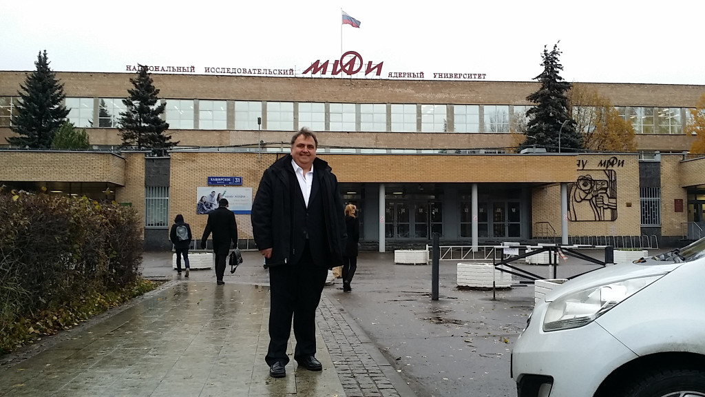
Below is a picture of MEPhI outside. The word “nuclear” reminds that there is a nuclear reactor in the Moscow Engineering Physics Institute, so it’s hard to get there, especially with an American passport - I got a pass for two weeks, and the rector signed the order for the seminar. At the entrance there is a machine gunner with Kalashnikov (!)
(I was not allowed to photograph the machine gunner )
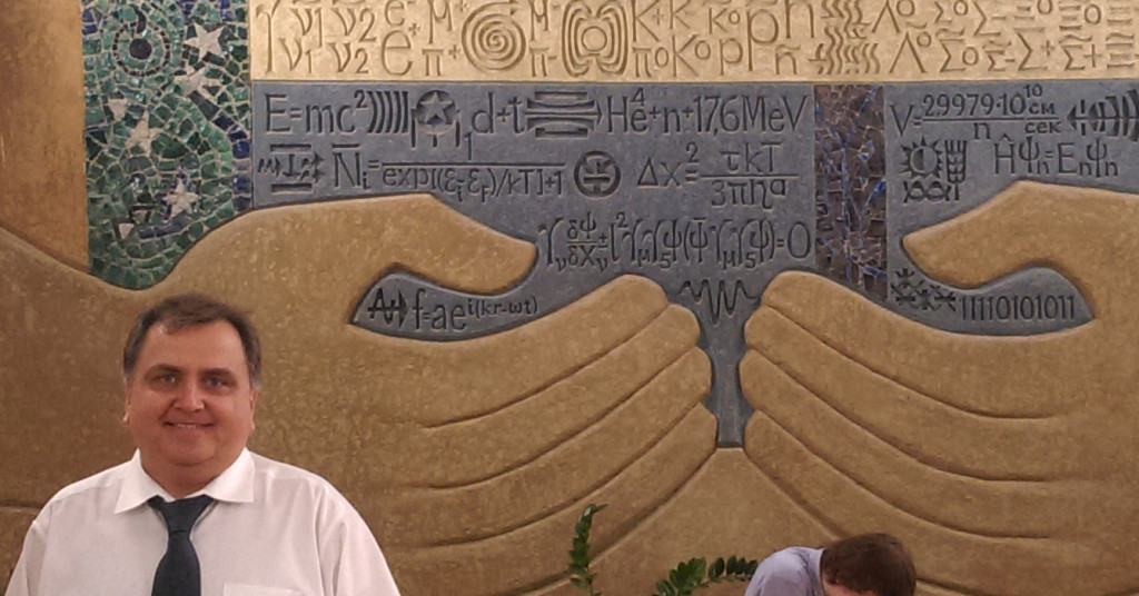
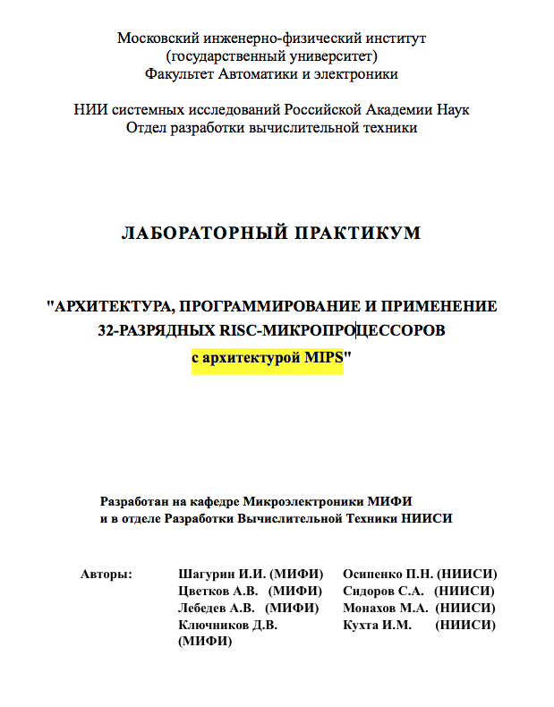
Here I am (Yuri Panchul) with other organizers of the seminar - Igor Ivanovich Shagurin and Maxim Gorbunov: Igor Ivanovich Shagurin, deputy. Head of the Department of Micro- and Nanoelectronics - author of books and articles on microprocessors Intel, Motorola and PowerPC, laboratory work on MIPS . UPD: Clarification from a comrade from NIIIS:

Interestingly, Igor Ivanovich Shagurin went to represent Soviet electronics at a conference in San Francisco back in the 1970s, when the USSR was a fairly isolated country. The participants of that VLSI conference in the 1970s were taken to Muir Woods, the area with the highest Sequoia sempervirens sequoias on earth, Maxim Gorbunov , a researcher from NIIISI / SRISA , an institute that is also involved in the development of Russian microprocessors with MIPS architecture - COMDIV-32 and COMMISSION-64. Maxim specializes in designing the topology of radiation-resistant VLSI and was co-chair of one of the sections of the international conference RADECS in Moscow:


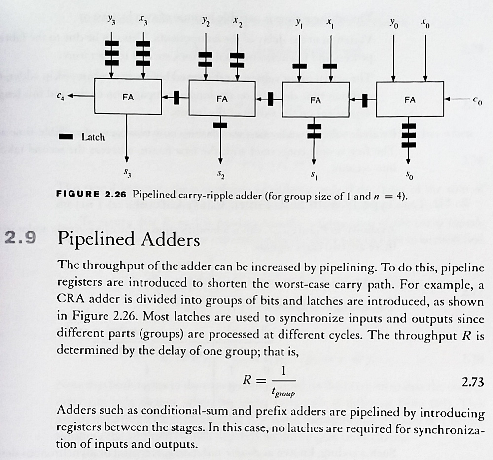
Before the MIPSfpga seminar at MEPhI, one of the instructors, Yegor Kuzmin, began to ask me about the race conditions in a certain scheme for specialized computing that arose as a student project. I’m not sure that I understood it correctly, but expressed that in a properly organized synchronous design such problems do not arise and promised to send as an example a photograph of a page from the book “Digital Arithmetic”, which understands the organization of the pipeline adder, which contains a small amount of combinatorial logic (the same as in the adder with sequential carry), but at the same time places the registers (D-triggers) so that the adder can start a new addition operation every clock cycle, with a frequency clock signal, determined by the delay of a single-bit full combinational adder:
Digital Arithmetic 1st Edition by Milos D. Ercegovac and Tomás Lang At the same time I photographed a couple of pages about self-times asynchronous circuits, also related to the issue .
Then I was introduced to Vladimir Dementyev, who, together with Andrei Andrianov, Dmitry Kozlovsky, conducts laboratory classes at the MEPhI for programming Microchip PIC32MX microcontrollers. I told Vladimir that Professor Alex Dean from the University of North Carolina collaborated with Imagination, Microchip and Digilent and is now developing a new course on programming Microchip PIC32MZ microcontrollersThis course includes RTOSs and the newfangled connection of microcontrollers to the cloud. The PIC32MZ microcontroller is based on the MIPS microAptiv UP microprocessor core, the same as that used in MIPSfpga. Therefore, I began to campaign for MEPhI comrades to take part in a review and (if they like) beta testing of this course: But back to our seminar. The topic of the seminar was MIPSfpga. What it is:

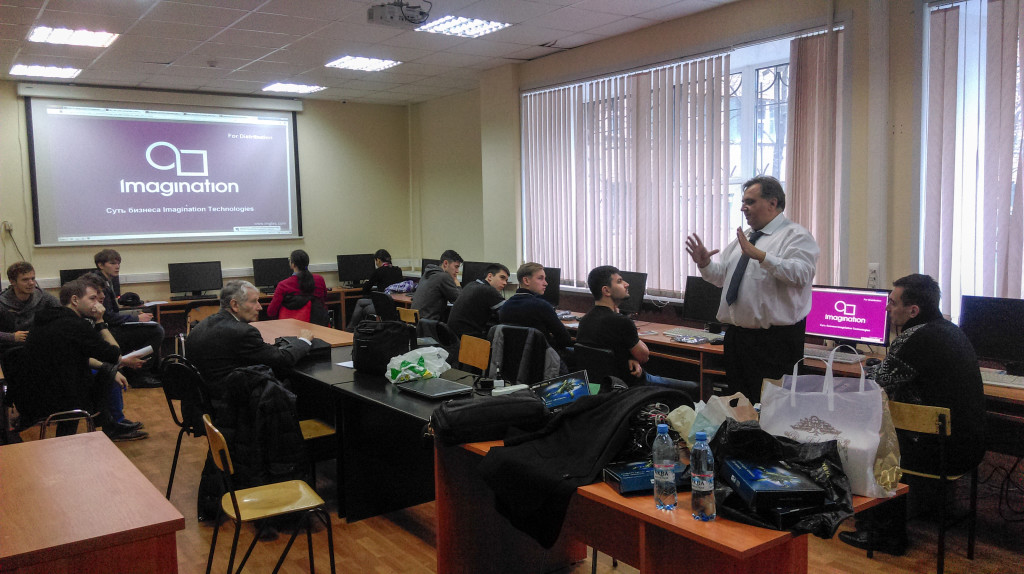
So, first I spoke and talked about:
1. Imagination Technologies and its MIPS business unit
2. Educational programs of Imagination Technologies
3. To refresh the concept of RTL-to-GDSII flow for those in the audience who did not have Verilog / VHDL to specialization: How IP blocks and systems on a chip (SoC) are designed.
4. I told a little about the three lines of MIPS microprocessor cores and in more detail about the line of microcontroller class cores, on the basis of one of which (MIPS microAptiv UP) the MIPSfpga
5 package was created . Since one of the exercises further included a demonstration of the cache, I said a couple words and about caches in MIPS microAptiv UP

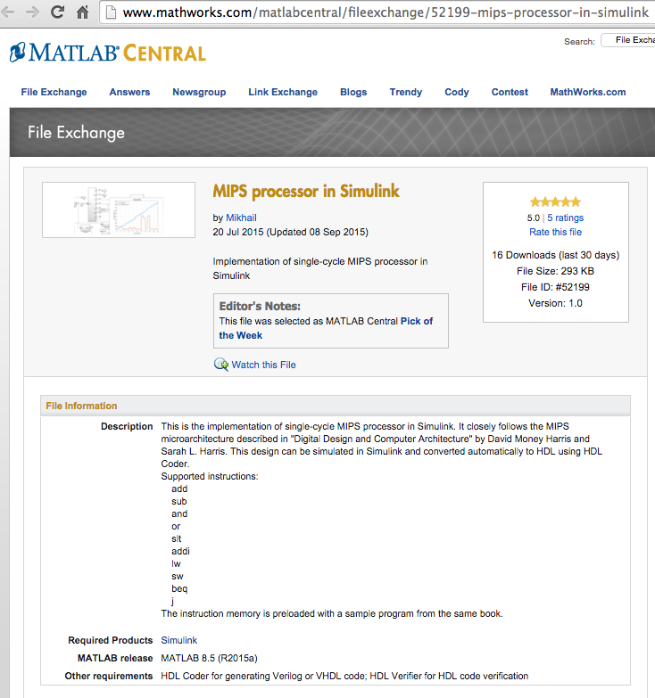
After my first speech, Mikhail Peselnik, a speaker from MathWorks made a speech: Mikhail Peselnik implemented a subset of MIPS on Simulink , which received a sort of editorial award MATLAB Central Pick of the Week: Michael’s example showed that for a student the architecture and microarchitecture of processor cores can be studied in different ways - at least on Verilog and VHDL, at least with the help of C models, at least with the help of Simulink. But after the basics of architecture and microarchitecture are studied, the student should experiment with an industrial processor, and here MIPSfpga enters the scene, with which:
But in order to experiment with SoC developments and with the kernel, they need to have a good command of the tool / implementation tool. Therefore, after Mikhail Mikhail Filippov, application engineer from Macro Group, an official representative of Xilinx in Russia, spoke. Xilinx is the company that once invented FPGAs and to this day remains # 1 in the most high-speed FPGAs.
Alexander Filippov made two reports:

What FPGA / FPGA is on my fingers I explained in another post on Habr - How to start developing iron using FPGAs - step by step instructions . But let us repeat this information again:
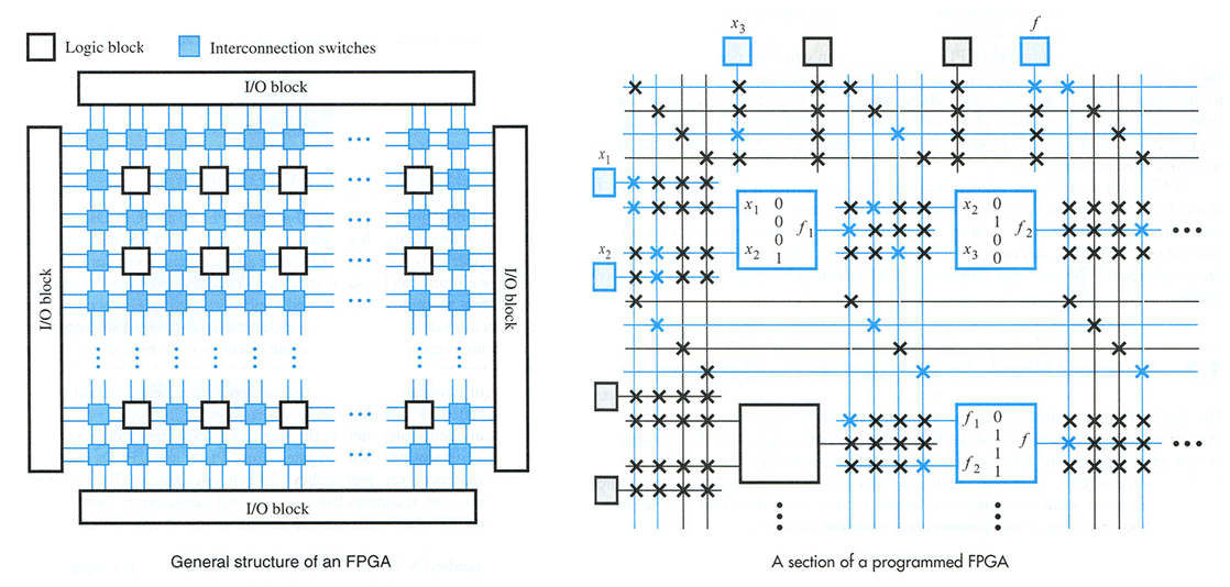
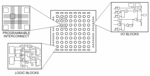
In the simplest version, the FPGA consists of a matrix of homogeneous cells, each of which can be changed into function using multiplexers connected to the bits of the configuration memory. One cell can become an AND gate with four inputs and one output, another - a single-bit register, etc. We load a sequence of bits from the memory into the configuration memory - and the given electronic circuit is formed in the FPGA, which can be a processor, display controller, etc.
FPGAs / FPGAs are not processors; by “programming” FPGAs (filling the configuration memory of FPGAs) you create an electronic circuit (hardware), while when programming a processor (fixed hardware) you slip a chain of sequential program instructions written into it (software).
Below is a diagram of the simplest FPGA unit, which includes a look-up table (LUT) and flip-flop. True, in this scheme, multiplexers that change the function of the cell, and connections to the configuration memory are not shown.

Diagrams illustrating the structure of FPGA:
And one more:
After lunch in the dining room of the Moscow Engineering Physics Institute, we began the practical part. Initially, when Imagination Technologies and Xilinx held such a seminar in Los Angeles, they usedslides prepared by professors David and Sarah Harris from southern California . As it originally looked, you can see on the video:
All 8 videos from a seminar in Los Angeles
For seminars in Russia, Harris's core and lab bindings had to be substantially modified. Modifications can be found at https://github.com/MIPSfpga/mipsfpga-plus . Differences include:
1. Everything is sorted for cheap motherboards from Altera, available in Russia without export-import engine
2. Implemented loading of the program into a synthesized system without using BusBlaster, simply via UART
3. Light sensor as a peripheral instead of an LCD display
4. Switchable ultra-low frequency clock signal, allowing labs to visualize the operation of any processor internals
5. Added a simple lab to visualize cache misses
+ every little thing and cosmetics - a more compact loader / bootloader, the possibility of narrow non-cacheable transactions to memory, etc.
Details:
1. Porting under Altera
First of all, Harris slides showed everything for Xilinx, and recently, shipping boards from Xilinx FPGAs to Russia has become a rather complicated bureaucratic procedure, taking 3-4 months. The same thing happened with the licensing of the software for synthesis and the place-and-route Xilinx Vivado, even with free licenses. Some Russian universities did not have Xilinx boards or Vivado licenses; others had only the old license for the predecessor of Vivado - the 2013 ISE software, which did not support FPGAs on boards that I transported across Russia.
In short, to conduct seminars in Russia, comrades and I, in California, had ported MIPSfpga to a couple of cheap boards available in Russia from Xilinx rival Altera (this company is now merging with Intel). Alter boards were donated for the needs of the workshop by the Zelenograd company SPC Elvis . The main board at MEPhI, MIPT and SSAU was the Terasic DE0-CV based on Altera Cyclone V: Another board was the Terasic DE0-Nano - a very compact shawl suitable for projects like flying robots, but with a small amount of peripherals on board: Terasic DE0- disadvantage Nano is a small number of peripheral devices on the board itself, but it is also an advantage, since DE0-Nano can be connected as a designer with other boards and built into different devices:


2. Download via UART The
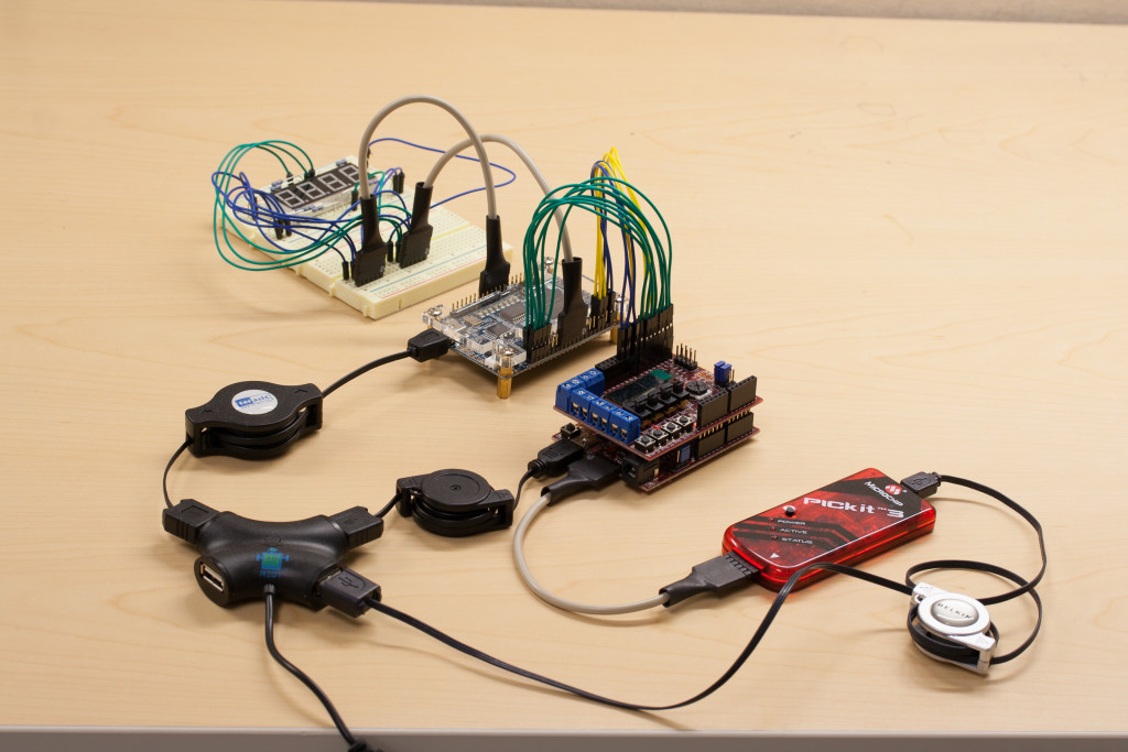
second slide problem from Harris was to use the Bus Blaster debug adapter and software for it called OpenOCD . Basically, BusBlaster / OpenOCD is a pretty good solution of its kind. It allows not only loading programs into the system synthesized inside the FPGA, but also debugging them remotely via the EJTAG interface, an add-in of a higher level over the JTAG interface. At the same time, BusBlaster costs only $ 43, which is much cheaper than industrial debugging EJTAG adapters.
Unfortunately, the BusBlaster / OpenOCD combination is rather crude, and I was afraid that it would not work on some unexpected computer configuration in Russia (I was right - it did not work at MIPT and SSAU). Besides,on a site that sells a BusBlaster / OpenOCD combination for MIPS , sometimes the boards run out.
For this and other reasons, I began to look for other ways to load software into the system (in the FPGA, you need to load separately the configuration / hardware and software for the processor (in a synthesized system with a processor)). Alexei anonymous Internet troll tried to take me weak for a long time, so that I would implement the EJTAG bootloader through Altera USB Blaster, but since I was not an EJTAG expert, I chose a simple solution that worked since the Soviet era - to load the program via the serial port / UART. True, during the Soviet era there was an RS-232C port, and in the 1990s chips from FTDI appeared, which made it possible to do everything through a USB cable connected to a PC. Different variations of such an adapter can be bought for $ 5 in Moscow and for less than $ 2 via the Internet from China:
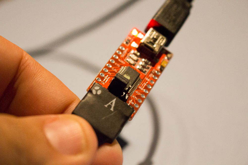
I’ll immediately notice that you can load programs into synthesized SoC in different ways. In one of them, more traditional, the system has a small fixed program in memory (bootloader), which starts after a reset (reset) of the system and loads a larger program through the UART / serial port. This method was used by Anton Pavlov from NIIIS, who demonstrated it at seminars at Moscow State University and Moscow Engineering Physics Institute, and also wrote a note about him on geektimes "MIPSfpga: outside the canon . "
I did the loading in an alternative way, in which the memory is filled with a state machine, fully implemented in the hardware. The machine accepts a text file in Motorola S-Record format from a PC via UART, parses it (everything in the hardware) and fills the memory with data, while the processor is in a reset state. Then the processor wakes up and starts reading the program from the system memory. All that needs to be done on the PC side is to convert the executable ELF file to the Motorola S-Record format and send it to the virtual COM port with the “type” windows-shell command.
3. The light sensor as a peripheral instead of an LCD display
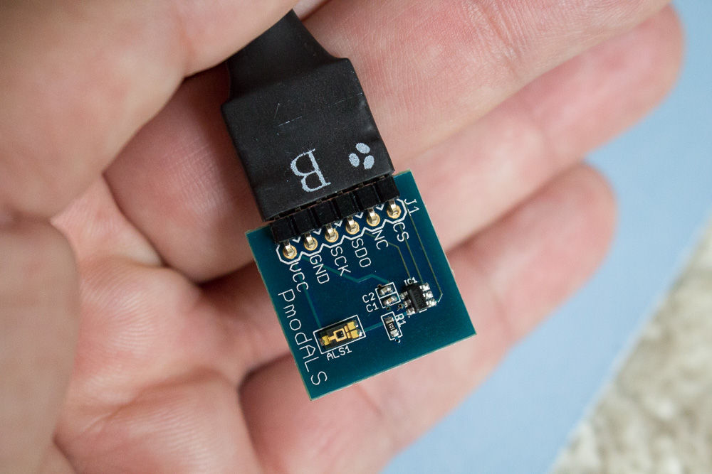
In the original Harris labs, they used a seven-segment indicator and an SPI LCD display as examples of peripheral devices. An example with a seven-segment indicator is boring - any student understands that if you know how to blink with one light, then you know how to blink with seven lights. The SPI example is a little better, especially if we are talking about novice students, but why do we need a second display if there is already a seven-segment indicator? In short, before going to Russia, I bought 20 light sensors, also with an SPI interface, and used them instead of displays: At the same time, the interface to it is very simple - here is the interface module I wrote (note: this code does not include all modifications of the system to pair it with AHB-Lite bus, so that the software sees the value):

4.
Clock switched to ultra-low frequency When MIPSfpga appeared and Russian university professors began to study it, some of them began to complain that the package in its original form is not very interesting for advanced students, since the labs prepared by David and Sarah Harris use a processor like a “black box”, just connecting devices to it. In other words, Harris completely ignored that the processor is given in the source code, and therefore it is possible to implement labs with it that would allow connections to be output from arbitrary processor registers (not only registers visible to the programmer, but generally from any D-triggers), to connect for example, to LEDs, and observe what happens to the processor when executing certain programs.
As you understand, in order to make such observations “live”, it is necessary to make the processor work at a very low clock frequency, for example, a clock per second. How to do it? The MIPS microAptiv UP core implemented in ASIC on 28 nm technology can operate at frequencies above 500 MHz, and on 65 nm technology over 300 MHz. When implemented on FPGAs, the frequencies are much lower, but still high - 50-60 MHz. The frequencies of the clock signal generators on the boards are 50-100 MHz, with the possibility of increasing or decreasing the frequency using a phase-locked loop (PLL) / phase-locked loop (PLL) .
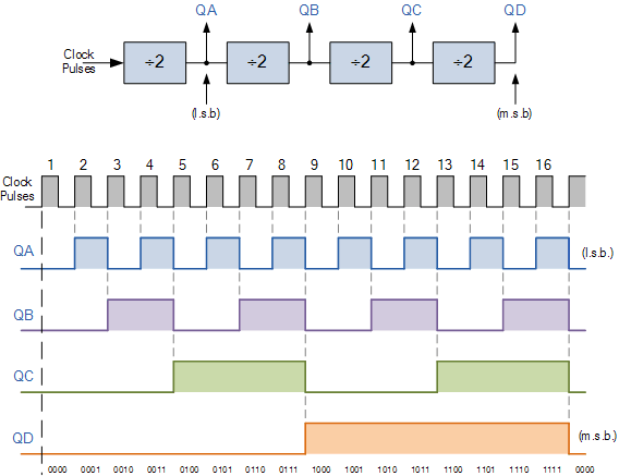
Unfortunately, using PLL, you can reduce the frequency to ~ 100 KHz, but you need to reduce the frequency to 1 Hz in another way. At first I tried to do this using a block from Altera calledALTCLKCTRL , but for some reason it did not work. Then I tried to divide the clock signal using a counter, but (I already knew that) this solution by itself does not work, because the synthesizer does not understand that the output signal is a clock signal and starts to split it incorrectly, as a result of which the processor does not work. I consulted with several comrades and we began to use the Alter macro “global” (and its equivalent on Xilinx BUFG). 5. Added a simple cache miss visualization lab
Now you can do interesting experiments - for example, to make the LED blink during a cache miss, and then observe in real time the cache hits and misses when filling a two-dimensional array. If you fill the array line by line, then the blinks will be different than if you fill in the columns: It should be noted that not everything went smoothly:
1. The GPIO in DE0-Nano is different from the GPIO in DE0-CV and Xilinx boards. In particular, for some reason I was unable to declare the entire GPIO port as one inout and then use its individual bits either as input or as output. Although on DE0-CV this goes fine. I didn’t have time to split the different GPIO outputs between different logical (on Verilog) signals, so I just didn’t sort the lab with the light sensor on DE0-Nano. For the same reason, I did not export the interface with the Bus Blaster to the DE0-CV.
2. Even worse, downloading via UART for DE0-Nano did not work at MEPhI, although before that it worked at Moscow State University and on my laptop. The reason is still not 100% clear:
2.1. Perhaps there was a problem of incompatibility of the Windows version (7 with the patch) and the USB-to-UART cable used for DE0-Nano. The cable was a cheap Chinese cable clone based on the PL2303TA chipset, although I did not try it before the seminar. It is known that the previous version of such cables based on chipsets with PL2303HX had a compatibility problem with Windows 8 ( see ). The most heinous that I had with me a laptop with a version of Windows 7, and a laptop with a version of Windows 8, and various alternatives to this cord. But I did not check all the combinations before the seminar, although I could have done it the previous evening - alas.
2.2. Two days before the workshop, I made changes to the clock divider. It was not worth doing either.
2.3. Well, at least everything worked well on the DE0-CV.
3. At MEPhI, I showed a more complex version of the cache example than before at Moscow State University. It was a mistake - in a complex example, the compiler optimized something, and the pattern of the lights was not as obvious as in the original simple example. The situation was somewhat saved by the invited additional speaker from NIIMI Anton Pavlov, who, although he did not have time at MEPhI, showed some present his own version of the MIPSfpga binding called myMIPSfpga, which he also described in the note "MIPSfpga: outside the canon . " Among other things, Anton has ported MIPSfpga to the Russian board Mars rover 3

which I, as a person tortured by export-import (Scylla: American export control + Charybdis: Russian customs), I’m going to try to use for the following educational events in Russia: During the break and after the seminar, Maxim Gorbunov showed me various mythical sights, which include three panels in the spirit of the era of the Andromeda Galaxy and Molecular Cafe of red and white multi-volume comes from 1960: UPD: As in the comments began to discuss mifishnuyu church, and I will make about it (I'm not inserted l This fragment was originally, as he was not sure that it is appropriate for geektimes):


I also went to the mythical church, around which there were so many screams on the Internet about three years ago, because of which employees even left the Moscow Engineering Physics Institute in protest. As a neutral person, i.e. a truly unbeliever, not a militant supporter of one or another side of the conflict, I must say that 1) the mythical church is rather modest and not vulgar, similar in spirit to the Orthodox Cathedral in San Francisco; 2) MEPhI is not the first Russian university with a religion, the course of Orthodoxy appeared at the Moscow Institute of Physics and Technology as early as 1988 (then the whole physics and technology college came to him, the students listened to the first lecture standing, but after three months there were no more than a dozen students); 3) there are churches in many American universities. To be continued.


Here I am (Yuri Panchul) with other organizers of the seminar - Igor Ivanovich Shagurin and Maxim Gorbunov: Igor Ivanovich Shagurin, deputy. Head of the Department of Micro- and Nanoelectronics - author of books and articles on microprocessors Intel, Motorola and PowerPC, laboratory work on MIPS . UPD: Clarification from a comrade from NIIIS:


“Writing that KOMDIV-32 and KOMDIV-64 have a MIPS architecture is not entirely correct (otherwise we would have written :)). We usually write that DOM is a MIPS-like architecture and command system. We can translate RISC processor instructions into our code, this is done in hardware. Yes, and the similarity applies to the old MIPS-I architecture. A very annoying inaccuracy was made in the Shagurin laboratory with the co-authors that you mentioned, due to the fact that MIPS processors were not available at that time, so the labs on our processor did it. In short, please replace the “MIPS architecture” with an MIPS-like architecture. „
Interestingly, Igor Ivanovich Shagurin went to represent Soviet electronics at a conference in San Francisco back in the 1970s, when the USSR was a fairly isolated country. The participants of that VLSI conference in the 1970s were taken to Muir Woods, the area with the highest Sequoia sempervirens sequoias on earth, Maxim Gorbunov , a researcher from NIIISI / SRISA , an institute that is also involved in the development of Russian microprocessors with MIPS architecture - COMDIV-32 and COMMISSION-64. Maxim specializes in designing the topology of radiation-resistant VLSI and was co-chair of one of the sections of the international conference RADECS in Moscow:


Before the MIPSfpga seminar at MEPhI, one of the instructors, Yegor Kuzmin, began to ask me about the race conditions in a certain scheme for specialized computing that arose as a student project. I’m not sure that I understood it correctly, but expressed that in a properly organized synchronous design such problems do not arise and promised to send as an example a photograph of a page from the book “Digital Arithmetic”, which understands the organization of the pipeline adder, which contains a small amount of combinatorial logic (the same as in the adder with sequential carry), but at the same time places the registers (D-triggers) so that the adder can start a new addition operation every clock cycle, with a frequency clock signal, determined by the delay of a single-bit full combinational adder:
Digital Arithmetic 1st Edition by Milos D. Ercegovac and Tomás Lang At the same time I photographed a couple of pages about self-times asynchronous circuits, also related to the issue .

Then I was introduced to Vladimir Dementyev, who, together with Andrei Andrianov, Dmitry Kozlovsky, conducts laboratory classes at the MEPhI for programming Microchip PIC32MX microcontrollers. I told Vladimir that Professor Alex Dean from the University of North Carolina collaborated with Imagination, Microchip and Digilent and is now developing a new course on programming Microchip PIC32MZ microcontrollersThis course includes RTOSs and the newfangled connection of microcontrollers to the cloud. The PIC32MZ microcontroller is based on the MIPS microAptiv UP microprocessor core, the same as that used in MIPSfpga. Therefore, I began to campaign for MEPhI comrades to take part in a review and (if they like) beta testing of this course: But back to our seminar. The topic of the seminar was MIPSfpga. What it is:

MIPSfpga - Free source licensed for universities MIPS microAptiv UP industrial microprocessor core. This core is used as the basis of the Microchip PIC32MZ microcontroller, as well as the new platform for the “Internet of things” - Samsung Artik 1.
The MIPS microAptiv UP core is used in industry together with the standard chip design process for the last 25 years, in which the processor and other system components use the crystal is developed in the language of equipment description Verilog, after which the description, after several transformations, turns into a mask, according to which microcircuits are manufactured at the factory.
The educational version of MIPS microAptiv UP - MIPSfpga - uses an alternative implementation path: the system description turns into configuration files for low-cost student cards with user-programmable gate arrays (FPGAs), which are often called programmable logic integrated circuits (FPGAs) or Field Programmable Gate Array (FPGAs) .
So, first I spoke and talked about:
1. Imagination Technologies and its MIPS business unit
2. Educational programs of Imagination Technologies
3. To refresh the concept of RTL-to-GDSII flow for those in the audience who did not have Verilog / VHDL to specialization: How IP blocks and systems on a chip (SoC) are designed.
4. I told a little about the three lines of MIPS microprocessor cores and in more detail about the line of microcontroller class cores, on the basis of one of which (MIPS microAptiv UP) the MIPSfpga
5 package was created . Since one of the exercises further included a demonstration of the cache, I said a couple words and about caches in MIPS microAptiv UP


After my first speech, Mikhail Peselnik, a speaker from MathWorks made a speech: Mikhail Peselnik implemented a subset of MIPS on Simulink , which received a sort of editorial award MATLAB Central Pick of the Week: Michael’s example showed that for a student the architecture and microarchitecture of processor cores can be studied in different ways - at least on Verilog and VHDL, at least with the help of C models, at least with the help of Simulink. But after the basics of architecture and microarchitecture are studied, the student should experiment with an industrial processor, and here MIPSfpga enters the scene, with which:


- Students can build their own prototypes of systems on a chip, combining a microprocessor core, memory and I / O devices designed by them
- Internal registers can be connected to the output ports and output information about the current state of the processor pipeline, caches and memory management devices. After that, the processor can be started at a low clock frequency and watch its work "in slow motion".
- Students can experiment with their cache options, design multi-core systems with specialized coprocessors, and experiment with dividing tasks into hardware and software.
But in order to experiment with SoC developments and with the kernel, they need to have a good command of the tool / implementation tool. Therefore, after Mikhail Mikhail Filippov, application engineer from Macro Group, an official representative of Xilinx in Russia, spoke. Xilinx is the company that once invented FPGAs and to this day remains # 1 in the most high-speed FPGAs.
Alexander Filippov made two reports:
- New 7-Series FPGAs and MPSoC UltraScale - XILINX Products for Powerful Programmable Chip Systems
- XILINX VIVADO Design Environment for Creating Systems on a Chip

What FPGA / FPGA is on my fingers I explained in another post on Habr - How to start developing iron using FPGAs - step by step instructions . But let us repeat this information again:
In the simplest version, the FPGA consists of a matrix of homogeneous cells, each of which can be changed into function using multiplexers connected to the bits of the configuration memory. One cell can become an AND gate with four inputs and one output, another - a single-bit register, etc. We load a sequence of bits from the memory into the configuration memory - and the given electronic circuit is formed in the FPGA, which can be a processor, display controller, etc.
FPGAs / FPGAs are not processors; by “programming” FPGAs (filling the configuration memory of FPGAs) you create an electronic circuit (hardware), while when programming a processor (fixed hardware) you slip a chain of sequential program instructions written into it (software).
Below is a diagram of the simplest FPGA unit, which includes a look-up table (LUT) and flip-flop. True, in this scheme, multiplexers that change the function of the cell, and connections to the configuration memory are not shown.

Diagrams illustrating the structure of FPGA:

And one more:

After lunch in the dining room of the Moscow Engineering Physics Institute, we began the practical part. Initially, when Imagination Technologies and Xilinx held such a seminar in Los Angeles, they usedslides prepared by professors David and Sarah Harris from southern California . As it originally looked, you can see on the video:
All 8 videos from a seminar in Los Angeles
For seminars in Russia, Harris's core and lab bindings had to be substantially modified. Modifications can be found at https://github.com/MIPSfpga/mipsfpga-plus . Differences include:
1. Everything is sorted for cheap motherboards from Altera, available in Russia without export-import engine
2. Implemented loading of the program into a synthesized system without using BusBlaster, simply via UART
3. Light sensor as a peripheral instead of an LCD display
4. Switchable ultra-low frequency clock signal, allowing labs to visualize the operation of any processor internals
5. Added a simple lab to visualize cache misses
+ every little thing and cosmetics - a more compact loader / bootloader, the possibility of narrow non-cacheable transactions to memory, etc.
Details:
1. Porting under Altera
First of all, Harris slides showed everything for Xilinx, and recently, shipping boards from Xilinx FPGAs to Russia has become a rather complicated bureaucratic procedure, taking 3-4 months. The same thing happened with the licensing of the software for synthesis and the place-and-route Xilinx Vivado, even with free licenses. Some Russian universities did not have Xilinx boards or Vivado licenses; others had only the old license for the predecessor of Vivado - the 2013 ISE software, which did not support FPGAs on boards that I transported across Russia.
In short, to conduct seminars in Russia, comrades and I, in California, had ported MIPSfpga to a couple of cheap boards available in Russia from Xilinx rival Altera (this company is now merging with Intel). Alter boards were donated for the needs of the workshop by the Zelenograd company SPC Elvis . The main board at MEPhI, MIPT and SSAU was the Terasic DE0-CV based on Altera Cyclone V: Another board was the Terasic DE0-Nano - a very compact shawl suitable for projects like flying robots, but with a small amount of peripherals on board: Terasic DE0- disadvantage Nano is a small number of peripheral devices on the board itself, but it is also an advantage, since DE0-Nano can be connected as a designer with other boards and built into different devices:


2. Download via UART The
second slide problem from Harris was to use the Bus Blaster debug adapter and software for it called OpenOCD . Basically, BusBlaster / OpenOCD is a pretty good solution of its kind. It allows not only loading programs into the system synthesized inside the FPGA, but also debugging them remotely via the EJTAG interface, an add-in of a higher level over the JTAG interface. At the same time, BusBlaster costs only $ 43, which is much cheaper than industrial debugging EJTAG adapters.
Unfortunately, the BusBlaster / OpenOCD combination is rather crude, and I was afraid that it would not work on some unexpected computer configuration in Russia (I was right - it did not work at MIPT and SSAU). Besides,on a site that sells a BusBlaster / OpenOCD combination for MIPS , sometimes the boards run out.
For this and other reasons, I began to look for other ways to load software into the system (in the FPGA, you need to load separately the configuration / hardware and software for the processor (in a synthesized system with a processor)). Alexei anonymous Internet troll tried to take me weak for a long time, so that I would implement the EJTAG bootloader through Altera USB Blaster, but since I was not an EJTAG expert, I chose a simple solution that worked since the Soviet era - to load the program via the serial port / UART. True, during the Soviet era there was an RS-232C port, and in the 1990s chips from FTDI appeared, which made it possible to do everything through a USB cable connected to a PC. Different variations of such an adapter can be bought for $ 5 in Moscow and for less than $ 2 via the Internet from China:

I’ll immediately notice that you can load programs into synthesized SoC in different ways. In one of them, more traditional, the system has a small fixed program in memory (bootloader), which starts after a reset (reset) of the system and loads a larger program through the UART / serial port. This method was used by Anton Pavlov from NIIIS, who demonstrated it at seminars at Moscow State University and Moscow Engineering Physics Institute, and also wrote a note about him on geektimes "MIPSfpga: outside the canon . "
I did the loading in an alternative way, in which the memory is filled with a state machine, fully implemented in the hardware. The machine accepts a text file in Motorola S-Record format from a PC via UART, parses it (everything in the hardware) and fills the memory with data, while the processor is in a reset state. Then the processor wakes up and starts reading the program from the system memory. All that needs to be done on the PC side is to convert the executable ELF file to the Motorola S-Record format and send it to the virtual COM port with the “type” windows-shell command.
3. The light sensor as a peripheral instead of an LCD display
In the original Harris labs, they used a seven-segment indicator and an SPI LCD display as examples of peripheral devices. An example with a seven-segment indicator is boring - any student understands that if you know how to blink with one light, then you know how to blink with seven lights. The SPI example is a little better, especially if we are talking about novice students, but why do we need a second display if there is already a seven-segment indicator? In short, before going to Russia, I bought 20 light sensors, also with an SPI interface, and used them instead of displays: At the same time, the interface to it is very simple - here is the interface module I wrote (note: this code does not include all modifications of the system to pair it with AHB-Lite bus, so that the software sees the value):


4.
Clock switched to ultra-low frequency When MIPSfpga appeared and Russian university professors began to study it, some of them began to complain that the package in its original form is not very interesting for advanced students, since the labs prepared by David and Sarah Harris use a processor like a “black box”, just connecting devices to it. In other words, Harris completely ignored that the processor is given in the source code, and therefore it is possible to implement labs with it that would allow connections to be output from arbitrary processor registers (not only registers visible to the programmer, but generally from any D-triggers), to connect for example, to LEDs, and observe what happens to the processor when executing certain programs.
As you understand, in order to make such observations “live”, it is necessary to make the processor work at a very low clock frequency, for example, a clock per second. How to do it? The MIPS microAptiv UP core implemented in ASIC on 28 nm technology can operate at frequencies above 500 MHz, and on 65 nm technology over 300 MHz. When implemented on FPGAs, the frequencies are much lower, but still high - 50-60 MHz. The frequencies of the clock signal generators on the boards are 50-100 MHz, with the possibility of increasing or decreasing the frequency using a phase-locked loop (PLL) / phase-locked loop (PLL) .
Unfortunately, using PLL, you can reduce the frequency to ~ 100 KHz, but you need to reduce the frequency to 1 Hz in another way. At first I tried to do this using a block from Altera calledALTCLKCTRL , but for some reason it did not work. Then I tried to divide the clock signal using a counter, but (I already knew that) this solution by itself does not work, because the synthesizer does not understand that the output signal is a clock signal and starts to split it incorrectly, as a result of which the processor does not work. I consulted with several comrades and we began to use the Alter macro “global” (and its equivalent on Xilinx BUFG). 5. Added a simple cache miss visualization lab

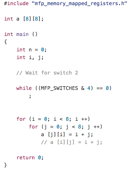
Now you can do interesting experiments - for example, to make the LED blink during a cache miss, and then observe in real time the cache hits and misses when filling a two-dimensional array. If you fill the array line by line, then the blinks will be different than if you fill in the columns: It should be noted that not everything went smoothly:

1. The GPIO in DE0-Nano is different from the GPIO in DE0-CV and Xilinx boards. In particular, for some reason I was unable to declare the entire GPIO port as one inout and then use its individual bits either as input or as output. Although on DE0-CV this goes fine. I didn’t have time to split the different GPIO outputs between different logical (on Verilog) signals, so I just didn’t sort the lab with the light sensor on DE0-Nano. For the same reason, I did not export the interface with the Bus Blaster to the DE0-CV.
2. Even worse, downloading via UART for DE0-Nano did not work at MEPhI, although before that it worked at Moscow State University and on my laptop. The reason is still not 100% clear:
2.1. Perhaps there was a problem of incompatibility of the Windows version (7 with the patch) and the USB-to-UART cable used for DE0-Nano. The cable was a cheap Chinese cable clone based on the PL2303TA chipset, although I did not try it before the seminar. It is known that the previous version of such cables based on chipsets with PL2303HX had a compatibility problem with Windows 8 ( see ). The most heinous that I had with me a laptop with a version of Windows 7, and a laptop with a version of Windows 8, and various alternatives to this cord. But I did not check all the combinations before the seminar, although I could have done it the previous evening - alas.
2.2. Two days before the workshop, I made changes to the clock divider. It was not worth doing either.
2.3. Well, at least everything worked well on the DE0-CV.
3. At MEPhI, I showed a more complex version of the cache example than before at Moscow State University. It was a mistake - in a complex example, the compiler optimized something, and the pattern of the lights was not as obvious as in the original simple example. The situation was somewhat saved by the invited additional speaker from NIIMI Anton Pavlov, who, although he did not have time at MEPhI, showed some present his own version of the MIPSfpga binding called myMIPSfpga, which he also described in the note "MIPSfpga: outside the canon . " Among other things, Anton has ported MIPSfpga to the Russian board Mars rover 3

which I, as a person tortured by export-import (Scylla: American export control + Charybdis: Russian customs), I’m going to try to use for the following educational events in Russia: During the break and after the seminar, Maxim Gorbunov showed me various mythical sights, which include three panels in the spirit of the era of the Andromeda Galaxy and Molecular Cafe of red and white multi-volume comes from 1960: UPD: As in the comments began to discuss mifishnuyu church, and I will make about it (I'm not inserted l This fragment was originally, as he was not sure that it is appropriate for geektimes):


I also went to the mythical church, around which there were so many screams on the Internet about three years ago, because of which employees even left the Moscow Engineering Physics Institute in protest. As a neutral person, i.e. a truly unbeliever, not a militant supporter of one or another side of the conflict, I must say that 1) the mythical church is rather modest and not vulgar, similar in spirit to the Orthodox Cathedral in San Francisco; 2) MEPhI is not the first Russian university with a religion, the course of Orthodoxy appeared at the Moscow Institute of Physics and Technology as early as 1988 (then the whole physics and technology college came to him, the students listened to the first lecture standing, but after three months there were no more than a dozen students); 3) there are churches in many American universities. To be continued.

Only registered users can participate in the survey. Please come in.
What do you think should be developed in the continuation of this post?
- 19.2% Arithmetic digital blocks 5
- 26.9% Asynchronous Logic 7
- 38.4% Design of digital logic at the level of register transfers in the hardware description language Verilog 10
- 11.5% Design of digital logic at the level of register transfers in the hardware description language VHDL 3
- 53.8% Methods for verification of digital circuits - SystemVerilog, UVM, Specman e, etc. 14
- 46.1% Microarchitecture (conveyor structure, block organization) of microprocessor cores 12
- 30.7% Add instructions to the kernel, interfaces for expanding processors 8
- 26.9% Multi-core systems (with or without coherence) 7
- 23% Architecture and use of FPGAs / FPGAs with a slope in Xilinx 6
- 34.6% Architecture and use of FPGAs / FPGAs with a slope in Altera 9
- 23% Architecture / assembler, low-level programming 6
- 19.2% Peripherals of microcontrollers and embedded processors 5
- 15.3% Microcontroller and Embedded Processor Applications 4
- 26.9% University culture 7
- 19.2% Educational programs of Imagination Technologies, Microchip Technology, Digilent / National Instruments and others 5
- 0% Other (explain in comments) 0
