July 11, 2016 at 00:07
How the "kettle" did UART <-> RS232 converter for Orange Pi
Introduction
It all started with the fact that I bought myself an Orange Pi, succumbing to the advertising slogan "analogue of the Rasberi Pi for only $ 15." The device was ordered by aliexpress and arrived in fifteen days in February. Then all the necessary additional components were bought: a radiator for the processor, a 15-watt power supply, a 32 GB micro SD card, an HDMI cable for connecting the monitor. For lack of time, he was gathering dust in a drawer until June. And finally, they got around to check its performance.
On standard firmware offered on the official website, the performance was not satisfactory. But standard firmwares do not suit me for the reason that I am so arranged - any device that falls into my hands must be customized according to the full program. Therefore, U-boot was picked up, the source code of which was downloaded from official FTP , as well as the assembly of Arch Linux for ARM . This reference manual for Banana Pi was taken as a reference manual and a starting point for digging .
After some simple manipulations (the description of which is more suitable for the Habr), both the bootloader and the archive were uploaded to the memory card and the device was turned on. However, after loading I was waiting for a black screen and a burning green LED on the "orange".
Well, it doesn’t matter, I thought. UART is soldered on the “orange”, I’ll connect as I terminal to it and see what happens. The necessary parts and wire were bought and such a cable was soldered here (picture under the spoiler)
Nubian version of the cable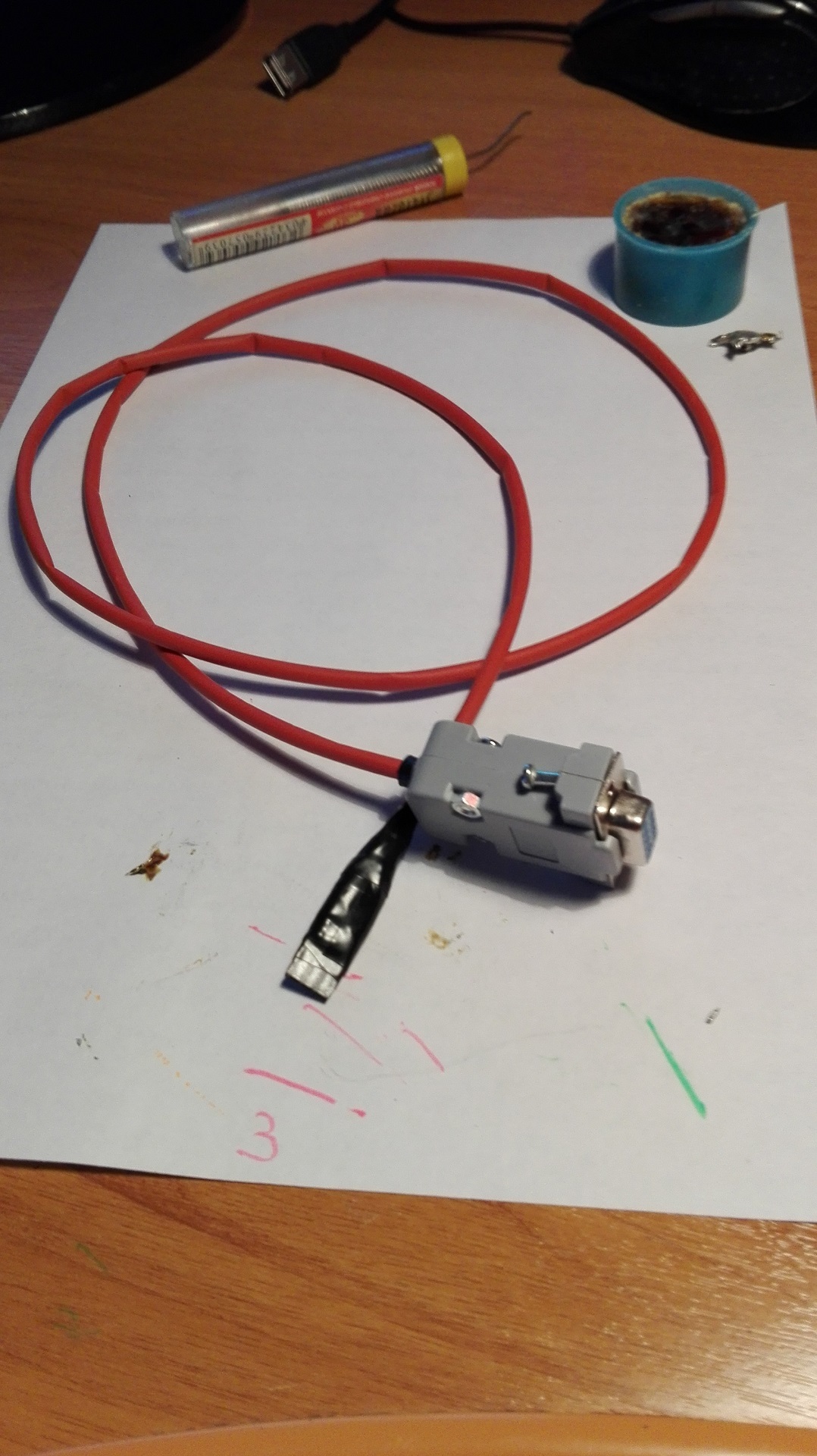
Anyone who is in the subject will immediately understand what I was wrong in making such a cable, and there are more than half of those reading. I suspected something was wrong after I saw krakozyabry who spit in my terminal "orange". It was the understanding of the cause of my stupid mistake that prompted me to the actions described below.
1. What is the difference between UART and RS232
The difference in levels. The serial interface implemented in Orange Pi and other similar devices is based on TTL logic, that is, the zero bit corresponds to the zero voltage level, and the unit level is +5 V. RS232 uses a higher voltage level, up to 15 V, and the unit corresponds to - 15 V, but zero +15 V. To increase the noise immunity of the channel, any voltage level below 3 V modulo is perceived as zero. The data transfer protocol in damage to the logical sequence of both UART and RS232 is exactly the same. All this is illustrated in the following byte transfer diagram.
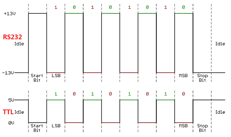
Here's how I could forget about it? When I was working at the Electric Locomotive Research Institute, I knew these things. And here, for some reason, nonsense froze. In general, it became clear that we need a certain level converter with signal inversion. The choice fell in the direction of connecting the entire economy to the COM port, which is on the motherboard of my home computer. Although of course you could look towards UART <-> USB, because the old serial interface is steadily losing relevance. However, my inclination towards simpler solutions won and, as a candidate for the acquisition, such a device surfaced
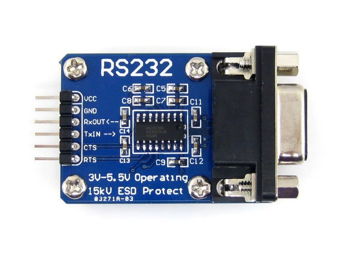
sold on the same "ali" for 464 rubles. In principle, this could be found in stores or on the radio market in my city, but the itch to do something with my hands was already awakened. Therefore, I rejected the thought of buying an interface card and decided to try to do it myself.
I must say that I'm actually friends with a soldering iron. At school and university, before buying the first computer, soldering all kinds of useful and not very nonsense was my main hobby. But I lived in a village, there were nineties. There wasn’t much money, the components were obtained by disassembling the radio trash that came into view. Books from the district library were the source of information - not everyone had “Internet” then. There was no rich instrument either. Foil textolite and ferric chloride were a legendary miracle. It was generally difficult.
After buying a computer, all the passion switched to it. And the skill of the soldering iron of small amplifiers-receivers is laid on the shelf. So I'm a “kettle." Therefore, to many of what I write below, I ask you to be lenient. And this article, by and large, for the same "dummies" as I am.
2. The choice of device circuit and its computer simulation
Find a scheme of such a device on the network once to spit. There are really many such schemes. The choice fell on this decision. The
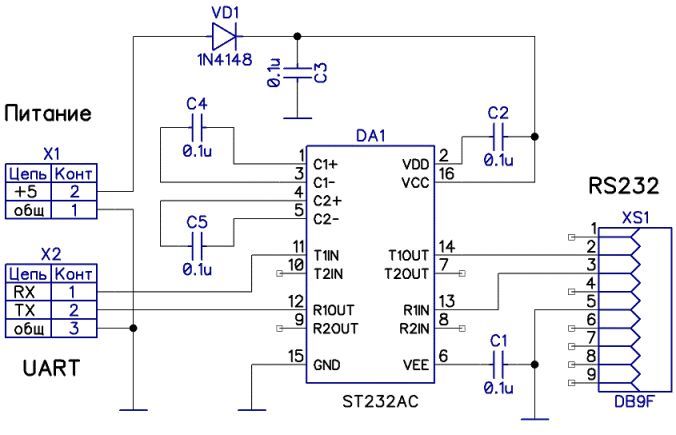
heart of the entire device is a MAX232 type microcircuit - a level converter operating on the principle of a “ charge pump ”. An increase in voltage from 5 V is carried out by alternately charging the external capacitors C4 and C5. At the moments of the signal output to RS232, these capacitors are connected in series, and the voltage accumulated in them is added. In reverse transmission, the chip operates as a divider. In both directions of signal transmission, it is inverted.
The diode VD1 plays the role of "protection against a fool" - it locks the power supply when voltage is applied the wrong polarity.
Before starting to manufacture the device, I decided to see how all this will work, so I started by modeling the future device in the Proteus environment. To test the circuit, a virtual stand was assembled.
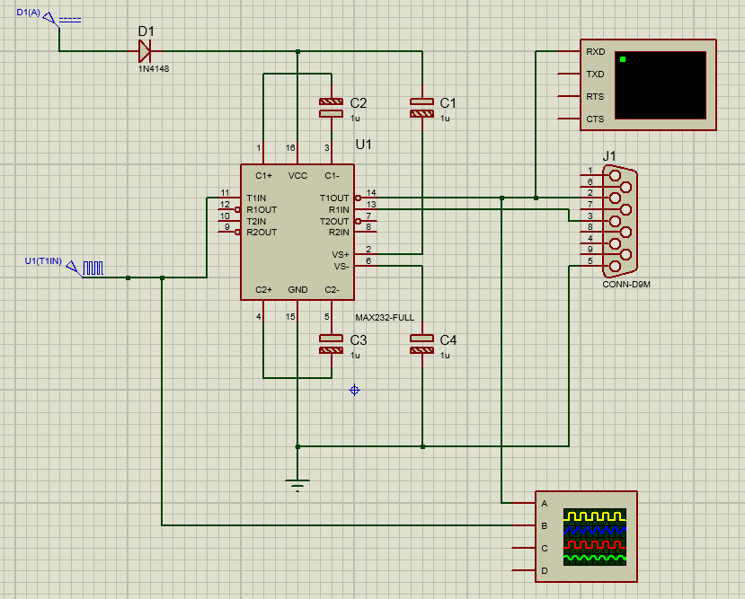
The first thing I wanted to do was to simulate everything, including the power circuit, since I was interested in the effect of the diode on the circuit's operation. By default, in Proteus, the power pins on the chips are hidden and pulled up to the plus of the desired level and ground. To unlock them, you must first display the hidden pins. To do this, go to the Template -> Set Design Colors menu
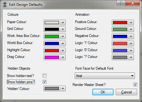
and select the Show hidded pins checkbox. Next, right-click on the chip and select the (most recent) Decompose item. The chip will be disassembled into separate parts. Double-clicking on the desired pin displays the window
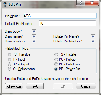
In which we put the daws Draw body and Draw Name. After that, select the entire microcircuit, including the text with which the outputs are signed and select the Make Device with the right menu button. We will be asked to select a name for the new device and save it. Everything, after this, the power circuits will be explicitly included in the simulation process.
Further, we will transmit something meaningful via UART, for example, the letter “A” encoded in ASCII code 65 in decimal, or the sequence 01000001b in binary. In addition, in order to initiate a transmission, it is necessary to send a start bit with a level of “0”, and to complete a transmission, send one or two stop bits with a level of “1”. Thus, the timing diagram of a frame transmitted over UART will look like this

To form such a signal, we use a source called Digital Pattern Generator (DPATTERN) with settings of the form. A

pulse width of 104 microseconds corresponds to a speed of 9600 baud. The waveform is specified by a string pattern where “L” means low and “F” means high. Accordingly, our line will look like "FLFLLLLLFLF". We will control the data received in RS232 with a virtual terminal, setting it up like this.
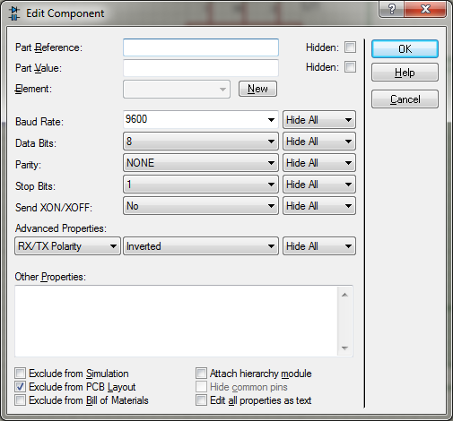
We will not use the parity bit, and we will use one stop bit. In addition, we say that the signal supplied to the terminal is inverted, which corresponds to the RS232 protocol. By starting the circuit simulation, we obtain a waveform of signals and output to a virtual terminal
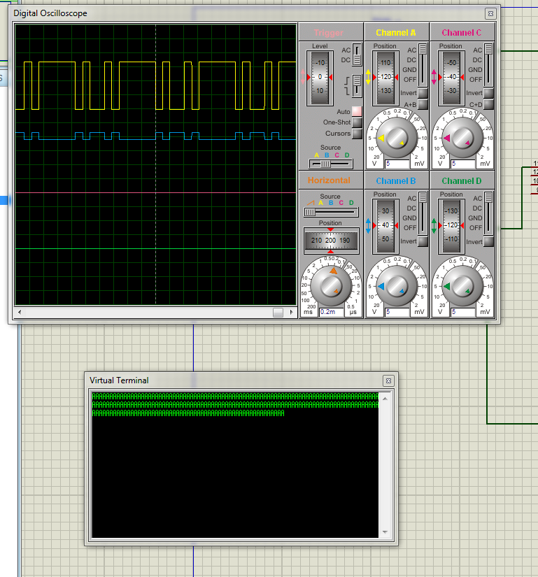
Channel A is the output signal supplied to the COM port. On channel B, the input TTL signal. The treasured letter "A" is displayed in the terminal. Thus, we are convinced that the proposed scheme is fully operational. In theory.
3. Selection and purchase of components
Of the stores closest to my habitat where you can get hold of radio components there are two that deserve attention: the Radio Parts store on Budenovsky Prospekt (this is the city of Rostov-on-Don) and the 1000 Radio Parts store on Nagibina Avenue, opposite Rio Shopping Center. The latter compares favorably with the fact that it has a website , although it’s quite ancient, and apparently lazily updated (and made on Joomla ...). Crawling along the price list, I picked up a list of what I need to buy.
I must say right away that I carefully avoided the SMD components in view of my inexperience. Therefore, I chose the MAX232CPE version for mounting in holes. The same took and electrolytes and a diode. However, it turned out that in the presence of only the MAX232CWE chip - the same thing, only ... SMD! Thinking for a second, I agreed with the seller’s proposal - we must start sometime ... There were no 15 V capacitors, but we found 100 V of the same capacity and the same dimensions. Well, nothing too. Instead of a DB-9 male connector, I was offered a mom. Thus we have the following list
| Position | Quantity, pcs | Cost, rub |
|---|---|---|
| MAX232CWE | 1 | 70 |
| Electrolytic capacitor, 1 uF x 100 V | 4 | fifteen |
| Diode 1N4148 | 1 | 5 |
| Socket DRB-09FA | 1 | 20 |
| Socket DB-9F | 1 | 20 |
| DB-9M plug | 1 | 20 |
| Housing for DB-9 Connector | 2 | 20 |
| Pins PLS-40 | 1 | fifteen |
| PLS-40 sockets | 1 | fifteen |
| Textolite unilateral 200 x 200 mm | 1 | 200 |
| Zapon varnish green, 30 ml | 1 | fifty |
| Ferric chloride 6 water, 250 g | 1 | 160 |
| Total : | 655 |
Ferric chloride, zapon varnish and textolite, of course, were not fully used. In addition, I did not include the purchased tool in this list: a simple soldering station (because before that I had only 40 watt soldering iron with a copper sting), side cutters and small pliers, metal scissors for cutting PCB, liquid rosin-alcohol flux LTI-120 well etc. In general, this saga cost me about 3,000 rubles.
In general, the components were purchased and brought home. 40-pin PLS pads were cut to the desired number of pins. One of the contacts is removed in order to ensure the uniqueness of the connection. The hole in the socket block corresponding to the removed pin is sealed with polyethylene.

4. Assembling the device on a breadboard and checking operation
In principle, for such a simple device this is not necessary. But I’m a “kettle”, so before making the board, I decided to check the circuit in real work.
The hardest thing was with the chip. To solder it to the breadboard, I had to pervert with soldering of twelve legs to the copper conductors. A monster spider about twelve legs came out.
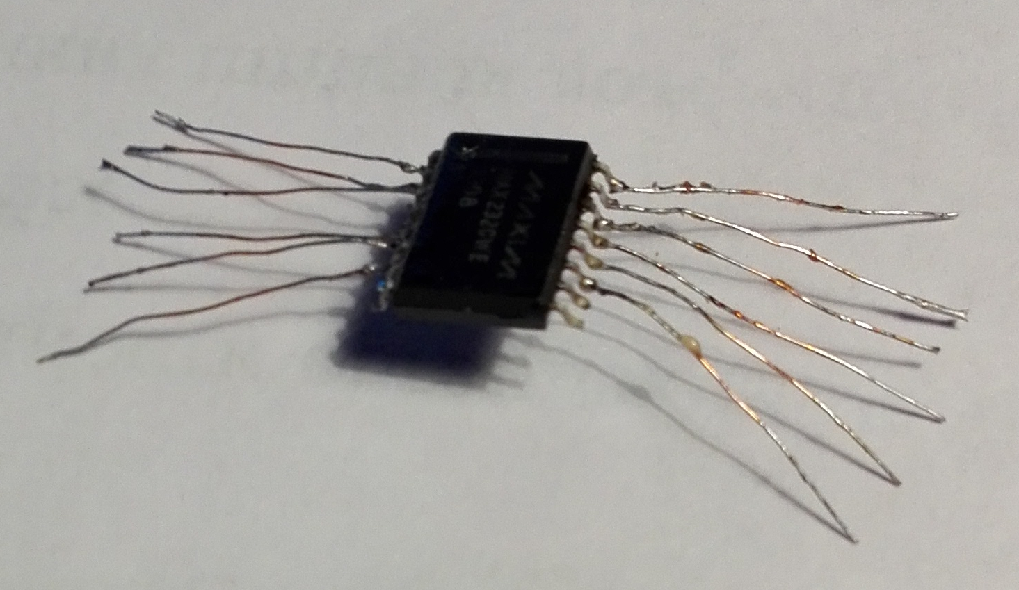
At that moment I understood two things: it’s good that I still bought a soldering station. But the bad thing is that I have to pretty tinker with this fineness. In general, the components were soldered to the "breadboard", the circuit was assembled with an "orange" board. +5 V power taken from the “orange” - 2nd pin on a two-row 40-pin pin block
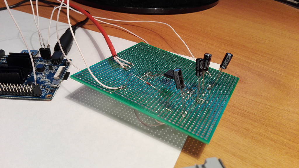
To connect to the device, the putty terminal was used, which is also available under Linux, and unlike minicom it has color output and does not require additional configuration for entering characters into the terminal from the keyboard.
In general, the board worked - the boot log lines ran across the terminal screen: first, from u-boot and then from the linux kernel. I

need to say how happy I was: firstly, the circuit works correctly, and secondly, Linux is installed on the “orange” true, it works normally in multi-user mode An

inoperative HDMI connector and the lack of an Ethernet interface, thus related to the configuration of the distribution itself. These problems, of course, will be solved, and this is not about them. Therefore, we move on to the next paragraph of the program
5. PCB layout
Made it in Altium Disigner. The wiring of the board is best done after the components are purchased. Perhaps, as in my case, you will need to install additional component libraries for Altium. The dimensions of the components and the topology of the footprint for each should correspond to the actual parts available. Here about me could not do without an unfortunate oversight, but more on that below.
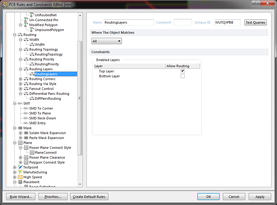
I will say right away - do not use automatic wiring. Perhaps this is customizable, but the auto-wiring tried to drag the track between the legs of the capacitors, which at a distance of 2 mm between them makes the track about a quarter millimeter wide, which was too cool for me as a “teapot”. Yes, and intuition suggested that such things should be avoided. Therefore, I used manual wiring (based on the results of automatic wiring), setting the road width to 0.5 mm in the wiring rules (Design -> Rules -> Routing -> Width)
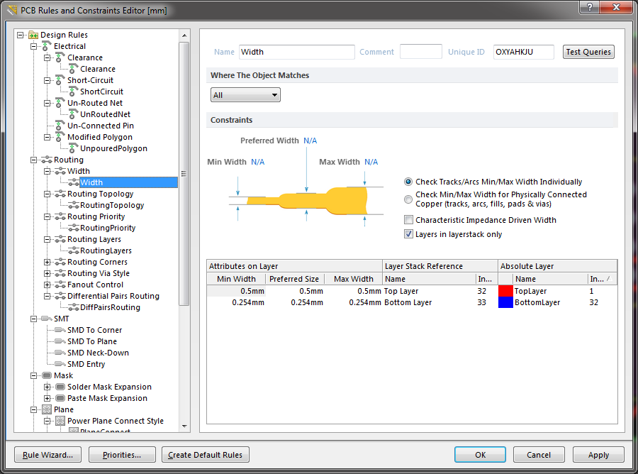
In addition, by default, Altium assumes that the board is two-layer. To force him to lay a single-sided board in the wiring rules, you should specify the wiring in one layer, say in Top Layer.
The circuit was typed in the circuit editor
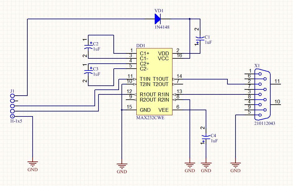
In this case, it is necessary to take into account the fact that the free unsoldered inputs of the microcircuit (legs 8 and 10) should be pulled to the ground, otherwise Altium will not compile the circuit for transferring it to the board editor.
As a result, through independent picking in the program and lessons from Alexey Sabunin, the goal was achieved and the board was divorced.
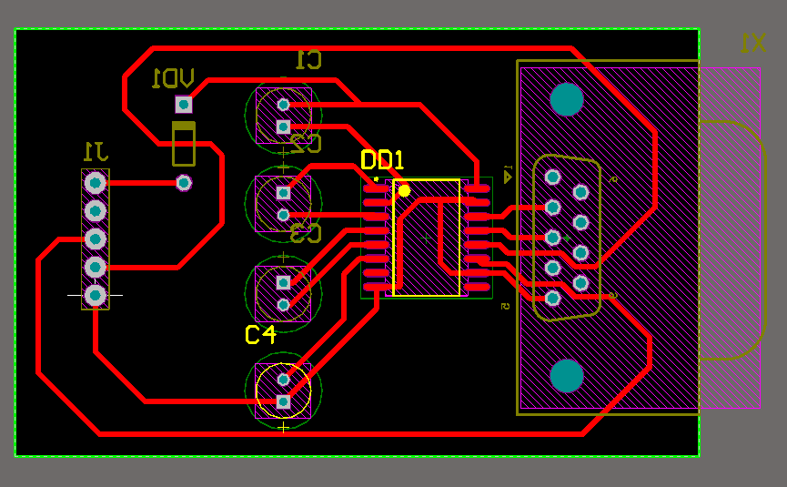
All components with mounting in the holes were located on the clean side of the PCB, and the microcircuit, due to the SMD performance, on the side of the tracks. To output the circuit layout to print, you must create a so-called Output Job File in the device project,
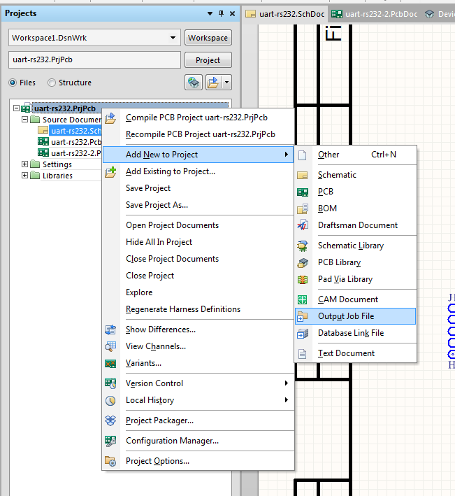
which is configured as follows. In the list of settings options, select Documentation Output and click on Add New Docimentation Outpu, choosing in the menu that appears PCB Prints and the board design for our device.
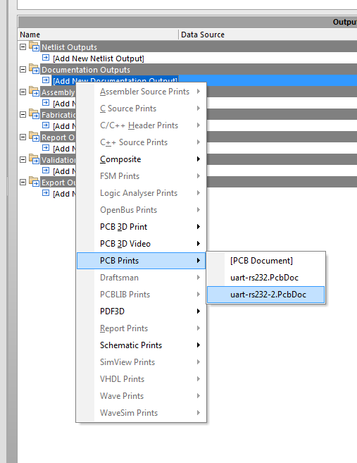
We rename the documentation item that appears, let's call it LUT, for transliteration of technology (LUT), which we are going to use to transfer the board's drawing to copper. Right-click on LUT and select Configure in the context menu. In the settings of the layers to be printed, we leave only two points: Top Layer and Multi-layer and arrange the jackdaws as shown in the screenshot.

Jackdaw Mirror is needed in particular to mirror the image on print. This is important, otherwise when you transfer the picture to copper, you get a mirror image of our tracks, but we don’t need it. In addition, you should look at Page Setup
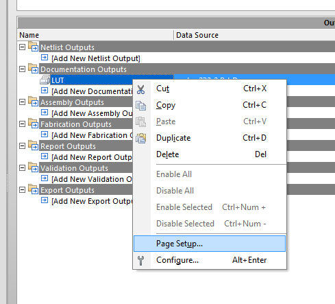
to select the paper size and pay attention to the scale factor (Scale). At the first print, it turned out to be 1.36 for some reason, but should be equal to one
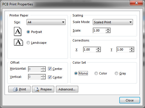
Now click Print. I don’t have my own printer, so I printed it in PDF using Foxit Reader, and then took the resulting file on a USB flash drive to the “sharashka” closest to me, in which I printed a picture on a glossy photo paper. As a result, it turned out this.
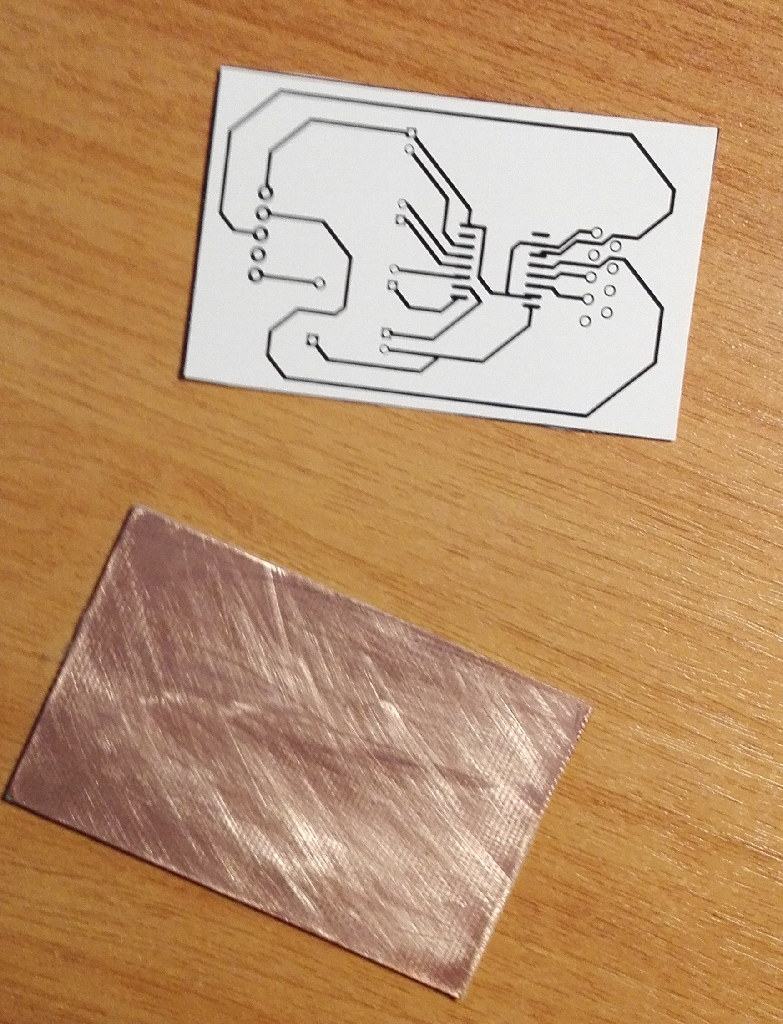
The board size came out 62 x 39 mm, a piece of PCB was cut out on this size with scissors for metal. Previously, I sawed textolite with a hacksaw and often (or rather always) it turned out terribly. Scissors come out evenly, without debris and damage to the conductive layer.
6. PCB manufacturing
The LUT method (laser-iron technology) was chosen because of its simplicity and accessibility. This article on Habré served as a guide to action . I tried not to violate the technology: I walked through the copper by zeroing, degreased, though not with acetone, because I could not find where to buy it, but with a universal white spirit degreaser, purchased at Lerua Merlin. He carefully and effortlessly ironed a sandwich of textolite and an iron pattern at maximum temperature. Either because I made a mistake somewhere, or because I didn’t let the workpiece cool down, or I just saved toner on the printer in “sharash”, it didn’t work out very well.
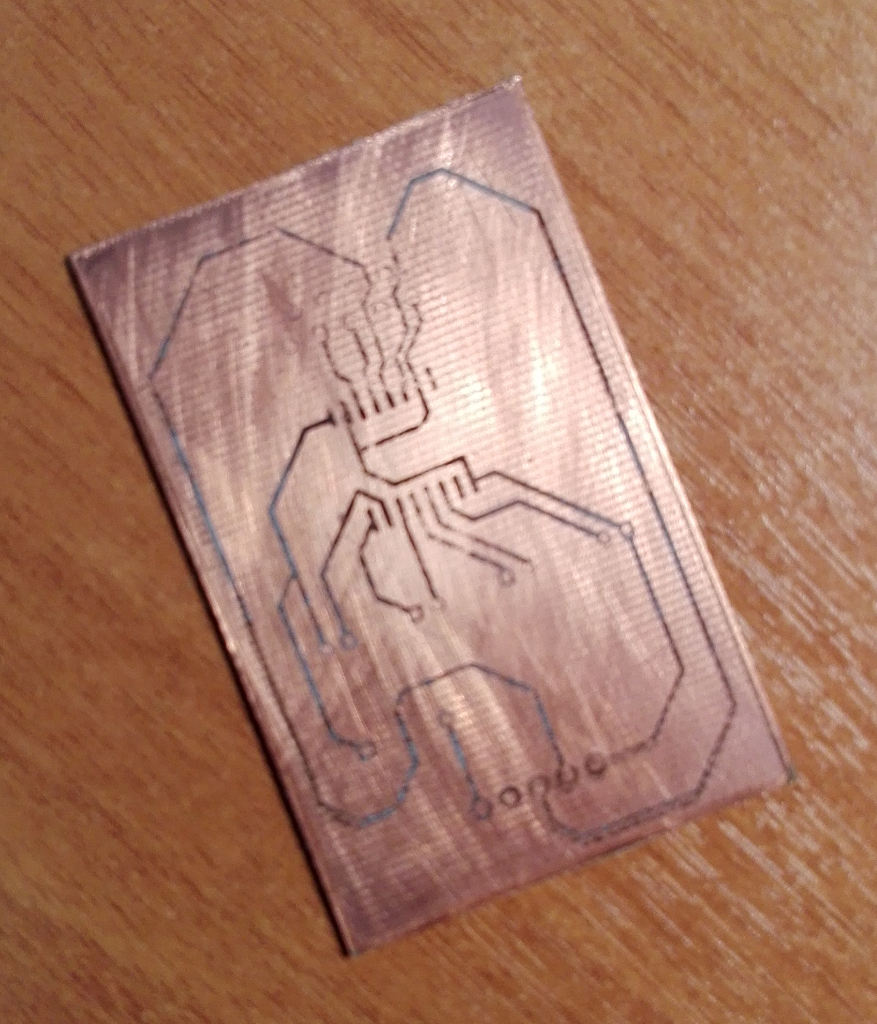
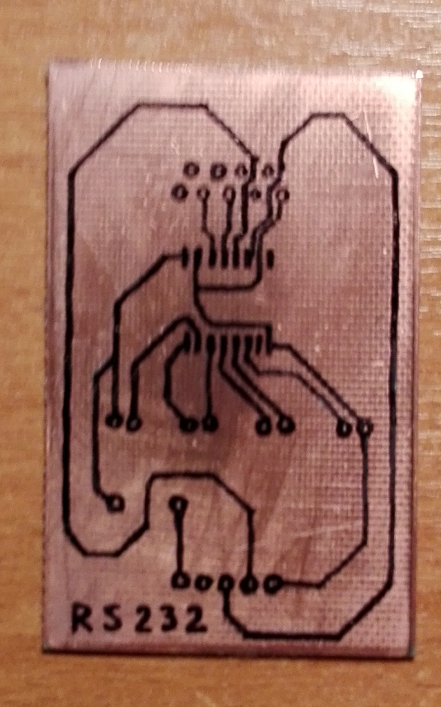
However, I prudently stocked up with the permanent marker Edding 404, which, not without the help of his beloved wife (with a pumped-up skill for summing up eyelashes and drawing patterns on the nails) circled all the tracks
Next, a solution of 6 aqueous ferric chloride was diluted at the rate of about 180 grams per 300 ml of water (I got hot water from the tap) and the board was thrown to be eaten into the etching cuvette. In order to poison the board and not poison his wife at the same time, the operation was performed at sunset on the balcony
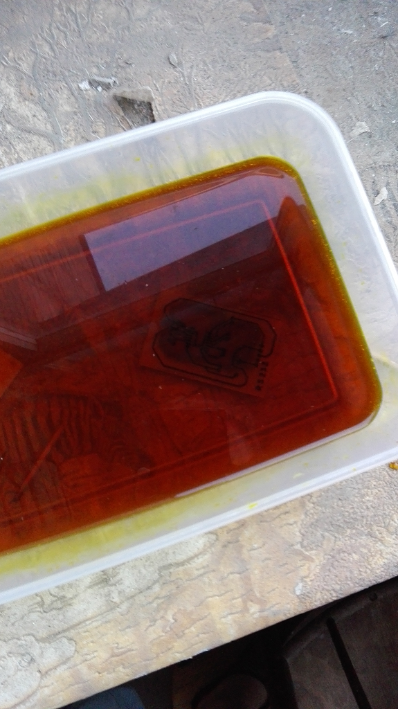
“Khlonyak” did not fail, there are rumors that they often sell low-quality ones. Etching took 13 minutes, the last islands of copper went right before our eyes. The main thing is not to forget to periodically kick the board with tweezers on the cuvette and monitor the process. As soon as the excess copper disappears, we take out the board urgently and rinse with a plentiful stream of water.
After washing, rubbing and drying, the moment of truth comes. It is necessary to remove the protective coating. I tried to make it white spirit,
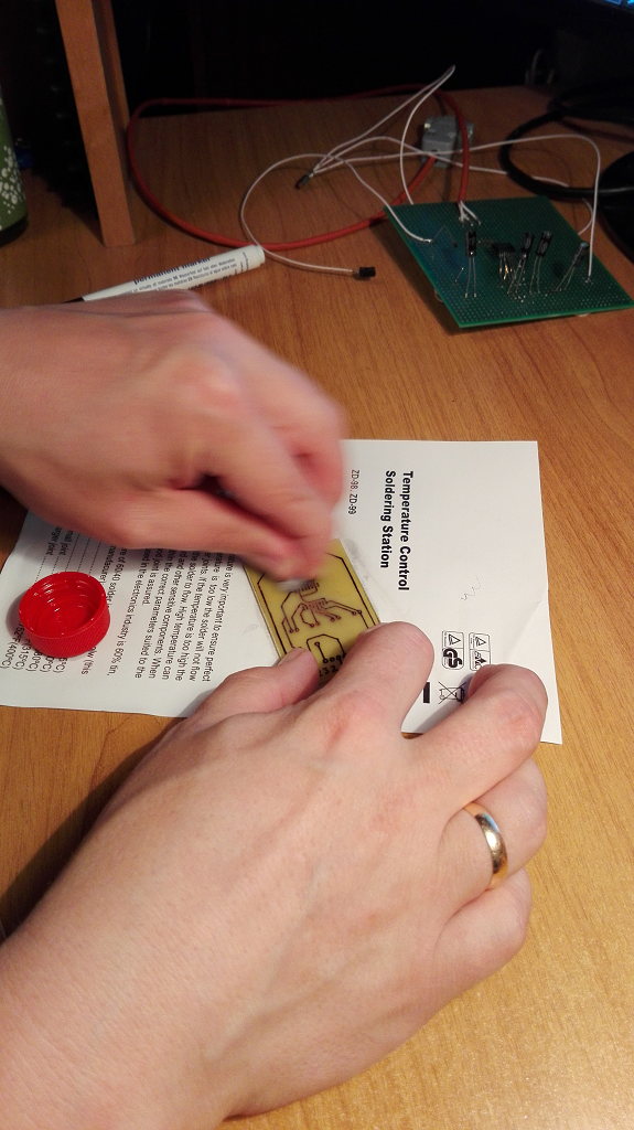
but things went tight. Then the wife offered her nail polish remover - this miraculous elixir washed off the coating instantly (I’m still terrified of what reagents our women use. Beauty is a terrible force!)
The marker didn’t fail - all the tracks survived

After cleaning the protective coating, you can start drilling holes. And here I made an unfortunate mistake - I didn’t have a 0.5 mm drill, and instead of postponing business until tomorrow, having bought the right drill, I hurried and took a millimeter, considering that it would work. As a result, I damaged many contact pads, fortunately not much and not irrevocably. But still, never rush. As my friend Mark from the laboratory of the Department of Mechatronics of the University of Munich, where I did the undergraduate practice “Dmitry, take a suitable tool for every job,” said. And he was right a thousand times.
7. Tinning of the board and soldering of components
Places for soldering components should be covered with a thin, shiny layer of solder. This is the main condition for successful work. I didn’t tackle the whole track. Firstly, I was afraid to distort them, and secondly, I was still going to cover the board with varnish. So I only irradiated the soldering spots. To do this, use a brush to apply rosin-alcohol flux LTI-120 and a soldering iron heated to 250-300 degrees, with a tiny drop of solder hanging from the tip of the flux, draw it to the desired points on the board. Due to the increase in the surface tension flux, the solder spreads over precisely the contact pads.
After that, the “breadboard” was dismantled, the wiring was removed from the microcircuit, and it was first soldered. Carefully place the chip with your hands or tweezers in its place in accordance with the pinout, so that each leg takes its place. Then grease the rows of legs with flux. With short and precise movements we touch all the legs in turn, not forgetting to collect solder on a soldering iron tip (but not too much, a small drop is enough). If everything is done correctly, then the legs are soldered to the site very quickly and accurately, without the "snot" and bridging the neighbors. It took me less than a minute to seal the microcircuit, and this is my first time doing it. Such a video inspired me on this feat , for which I am very grateful to its author. It turned out really not so scary.
Similarly, I figured out the rest of the details. The main thing here is to carefully trim the conclusions of the parts to the desired length - I left no more than a millimeter of output sticking out over the track, and bend them correctly and accurately, if necessary. Important, it is extremely important not to rush anywhere and do everything thoughtfully. As a result, it turned out what happened.
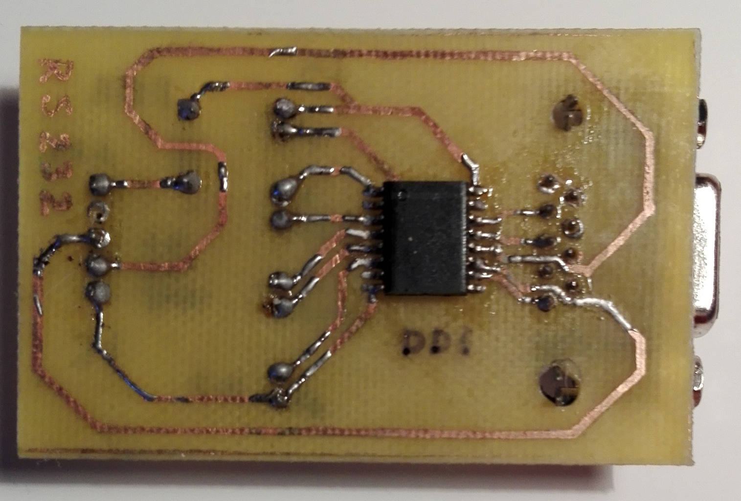
It was not possible to escape from the “snot”, but for the first time it turned out pretty tolerably, although they will probably criticize me.
8. Checking chains and another annoying mistake
After soldering, we wash off the entire flux with alcohol, take a multimeter in our hands and ring all the chains in order to check their conductivity and compliance with the circuit diagram. And here Byak crept unnoticed. The COM port connector was soldered in a mirror! "Earth" sat on the first leg instead of the fifth, Rx - on the fourth instead of the second.
Otherwise, the installation turned out to be correct, and I, having unzipped the connecting cables and tidying up the workplace, connected a brand new board to the "orange" and the computer.

The logs of the boot log ran again through the terminal window. I was happy!
9. Bringing "beauty"
In order to protect contacts from oxidation and make the device look “industrial”, the board was painted with green zapon lacquer. All marks applied before installation with a permanent marker were washed away with this very varnish. Well, okay ... Here's a photo of the finished product along with a set of cables.
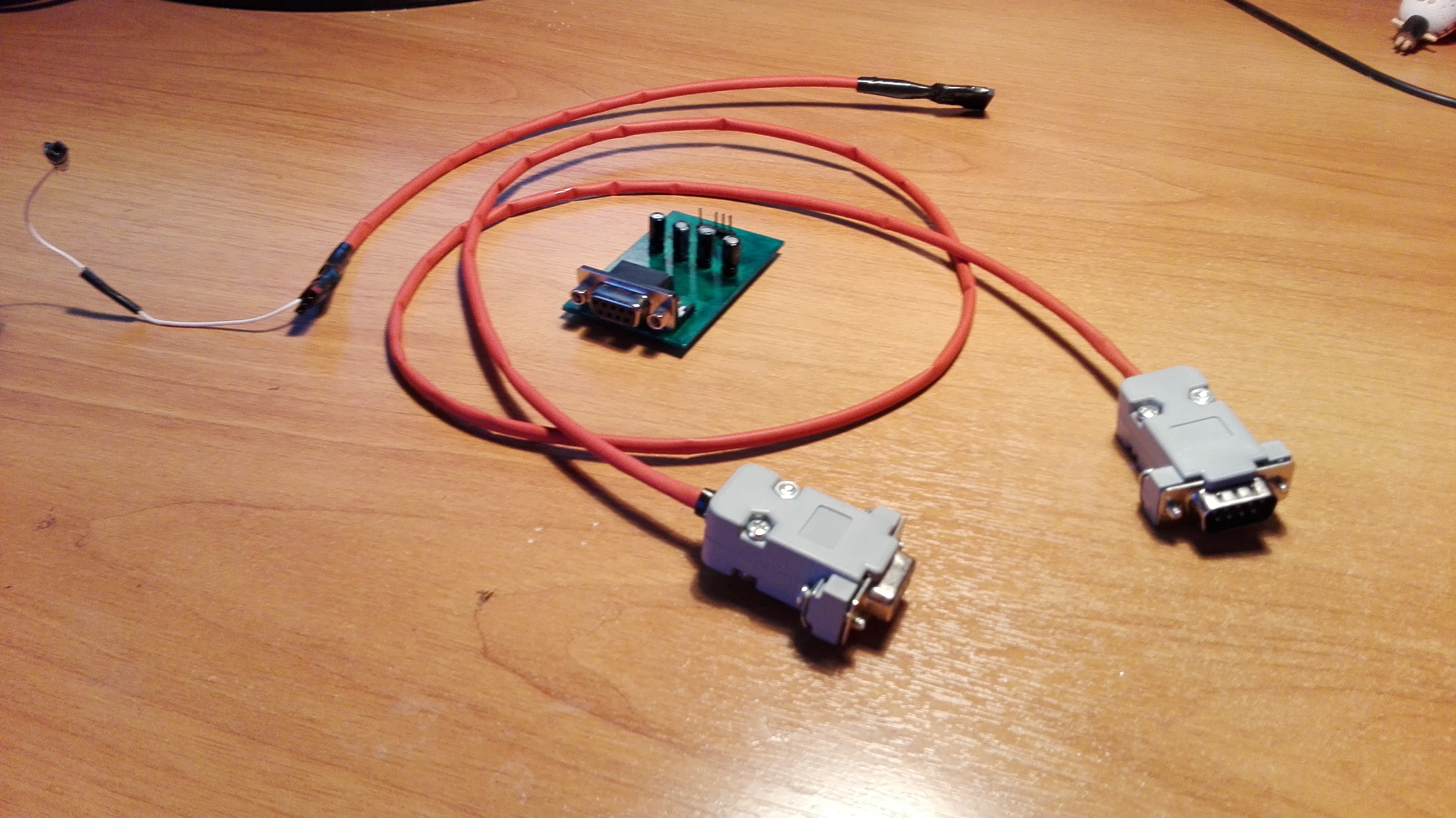
Now you can proceed to further refine the software for the "orange". Now I will not be blind and mute, but I can set up the system through a serial terminal.
Conclusion
That was interesting. Interesting for me, because for the first time. The first device designed on a computer and assembled on a printed circuit board with your own hands. And if someone smiles ironically, then let him remember that he also once did it for the first time ...
Thank you all for the attention paid to my writings!