Ultrafast thin-film transistors for future electronic devices developed
Welcome to the iCover Blog Pages ! Today we will dwell on an event that is significant for the whole world of microelectronics, namely, the creation of a new-generation thin-film transistor that works much faster than existing analogs.
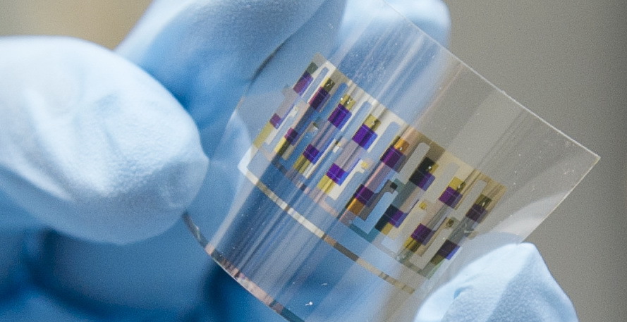
Extremely thin transparent thin-film transistors are one of the key components of an LCD TFT LCD. The cornerstone in improving the quality of the matrix remains the switching speed of the transistor, which is being improved in leading laboratories in the world. Korean scientists managed to create a thin-film transistor of electronic devices of the future, which works much faster than existing ones.
Thin-film transistors are nothing more than ordinary field-effect transistors, metal contacts and semiconductor conduction channels of which are represented by thin films with a thickness of 0.01 ... 0.01 microns. Being applied to the surface of glass or a transparent polymeric material, they are located as close as possible to pixel cells controlled by them, which ensures a stable contrast and saturated image, the absence of “tails” in moving objects, and the matrix reaction speed sufficient for comfortable work and relaxation.
The mobility of the movement of charge carriers in a semiconductor is equal to the speed of their movement, measured in centimeters per second, where one volt of voltage is applied to each centimeter of length. The lower the electrical resistance of the material, the faster the charges are able to move, which means that the faster the single thin-film transistors of which it consists will switch.
Joint research conducted by Samsung at Korea University and Samsung Advanced Institute of Technology proposed a new type of thin-film transistor with an order of magnitude faster than existing analogs. The launch of such a transistor in mass production will significantly increase the speed of LCD displays of televisions, smartphones and tablets with an active matrix TFT (Thin Film Transistor).
To obtain a transistor with similar technical characteristics, scientists used plasma from argon inert gas ions. Zinc oxynitride (ZnON) obtained by the method was used as the main component used to create the transistor.magnetron sputtering .
Compounds based on zinc oxide, as the basis for the creation of thin-film structures with a high speed of charge movement, have long been in the zone of special attention of scientists. At the same time, the main emphasis during the experiments was placed on doping (introducing a small amount of impurities) of the base material with cations of various metals — indium, gallium, hafnium, zirconium and lanthanides.
The speed limit for the movement of holes and electrons in the electric field of a semiconductor today reaches 5 to 20 cm2 / volt * sec, while ”... To ensure high performance and cost-effectiveness of electronic devices of the future, it is necessary to ensure the mobility of electric charge carriers over 100 cm2 / volt * sec ... ”- says Professor Sanghun Jeon from the National University of Korea. "The mobility of charge carriers in the zinc transistors we created is at least ten times higher than the mobility of carriers in conventional thin-film transistors."
The described result was obtained mainly due to the inclusion in the technological cycle of the stage of deposition of the material from a mixture of argon, oxygen (O2) and a mixture of nitrogen (N2). Alternating exposure to the zinc “substrate” with the listed gases at a constant pressure of nitrogen and argon and carefully controlled oxygen pressure within specified limits made it possible to form the thinnest (50 nm) film. Such high rates of charge carrier mobility in zinc oxynitride have become possible due to the filling of oxygen vacancies in the oxide structure with nitrogen. To obtain such a film in the presence of atmospheric oxygen, due to the low mutual activity of nitrogen and zinc, under conditions different from those proposed by specialists today is problematic.
In order to minimize the effect of oxygen on the proceeding reaction and increase the film strength, an argon plasma was used in the experiment, which, in addition to the “barrier” function, stimulated cascades of collisions of atoms and ions. Such artificial stimulation made it possible to redistribute the energy of chemical reactions and start the process of creating nanocrystals in the amorphous matrix - stable chemical compounds between nitrogen, zinc and oxygen.
The resulting zinc oxynitride film is characterized by a stable and uniform polycrystalline structure, resistant to active chemicals and radiation. During the test tests, the innovative film transistor and film transistor obtained in the traditional way were exposed to 30 days of atmospheric air. After a period of time, it turned out that the zinc oxynitride film, in contrast to the traditional one, practically did not lose its original properties. Measurement of the mobility of charge carriers showed that this parameter was 138 cm2 / volt * sec, which is an order of magnitude higher than the mobility of carriers in films obtained by the traditional method based on zinc oxide - gallium - indium.
Thus, the experimental results unequivocally confirmed a new absolute record for the mobility of electric charge carriers in a thin-film transistor based on zinc oxynitride ZnON.
Of course, despite the brilliant results of the experiment, which confirmed the effectiveness of the technology under consideration, conducting experiments in the laboratory significantly limited the capabilities of researchers, both in terms of obtaining the required level of repeatability of the results, and in terms of checking the potential of cations of other metals to improve already achieved indicators.
More information on the results of scientists can be found on the website Applied Physics Letters.
Dear readers, we are always happy to meet and wait for you on the iCover Blog Pages! We are ready to continue to please you with our publications and will try to do our best to ensure that the time spent with us is pleasing to you. And, of course, do not forget to subscribe to our sections and we promise - it won’t be boring!
Our other articles