UDB. What is it? Part 3. Datapath FIFO
- Transfer

We continue to translate Cypress’s proprietary documentation into UDB blocks. Moreover, everything is very well matched. To continue the practical article on UDB, we will need to use FIFO, and in the theoretical part we have chosen just the description of them. Therefore, we begin to study them in detail.
Previous articles in the cycle:
UDB. What is it? Part 1. Introduction. Pld.
UDB. What is it? Part 2. Datapath
21.3.2.2 Datapath FIFO
FIFO Modes and Configurations
Each FIFO buffer has several modes of operation and configurations available:
Table 21-2. FIFO modes and configurations.
| Mode | Description |
|---|---|
| Input / Output (input / output buffer) | In the input buffer mode, the CPU or DMA writes data to the FIFO, and the Datapath reads it. In the output buffer mode , the data gets into the FIFO from the Datapath, and the CPU or DMA reads them from there. |
| Buffer Single (single buffer) | FIFO works as a single buffer with no status. The data recorded in the FIFO is immediately readable and can be overwritten at any time. |
| Level / Edge (Level / drop) | The parameter responsible for loading the FIFO from Datapath can be triggered by level or by differential. |
| Normal / Fast (Normal / Fast) | The parameter responsible for loading the FIFO from the Datapath source : it is clocked with the clock source (normal) selected for Datapath or with the bus frequency (fast). This allows you to capture with the highest frequency in the system (bus frequency), regardless of the Datapath clock frequency. |
| Capture Software (program capture) | When this mode is on, and the FIFO is in the output buffer mode , reading the CPU or DMA of the associated battery (A0 for F0, A1 for F1), initializes the synchronous transfer of the battery value to the FIFO. The captured value is immediately readable from the FIFO. If chaining support is activated, the operation follows the chain to the MS block so that the Datapath can perform an atomic read of multibyte values. |
| Asynch (Asynchronous) | When the Datapach and system bus clock frequencies are not synchronized, the FIFO status signals can be forwarded to the rest of the Datapath either directly, clocked by the Datapath clock frequency, or with double synchronization, in Asynch mode. |
| Independent Clock Polarity (Independent Clock Polarity) | Each FIFO has a control bit to invert the polarity of the FIFO clock with respect to the Datapath clocking. |
Figure 21-7 shows the possible configuration options for the FIFO pair, depending on the Input / Output modes selected for each of them. If one FIFO is in input mode and the other in output mode, we get the RX / TX configuration. A typical example where such a configuration is needed is an SPI bus controller. In the Dual Capture configuration (both FIFOs are configured for output), independent capture of the A0 and A1 pairs or two independent captures of the A0 or A1 registers is provided. Finally, in Dual Buffer mode (both at the input), it is possible to use either the register pair or two independent registers for loading or comparing.

Figure 21-7. FIFO configurations.
Figure 21-8 details the sources and receivers for the FIFO.
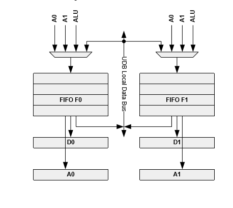
Figure 21-8. Sources and receivers FIFO.
When the FIFO operates in the input buffer mode, the source is the system bus, and the receivers are the Dx and Ax registers. When operating in the output buffer mode, the sources are the Ax and ALU registers, and the receiver is the system bus. The multiplexer selection is set statically in the UDB CFG15 configuration register, as shown in the table for F0_INSEL [1: 0] or F1_INSEL [1: 0]:
Table 21-3. The set of FIFO multiplexers in the UDB configuration register.
| Fx_INSEL [1: 0] | Description |
|---|---|
| 00 | Input Buffer Mode: The system bus is written to the FIFO, and the FIFO receiver is Ax or Dx. |
| 01 | Output buffer mode: the FIFO source is A0, and the FIFO receiver is the system bus. |
| ten | Output Buffer Mode: The FIFO source is A1, and the FIFO receiver is the system bus. |
| eleven | Output Buffer Mode: The FIFO source is the ALU output, and the FIFO receiver is the system bus. |
FIFO status
Each FIFO generates two status signals, “bus” and “block”, which are transmitted to UDB trace resources via the output multiplexer Datapath. The “bus” status can be used to trigger an interrupt or request a DMA read / write to the FIFO. The “block” state is mainly intended to transfer the state of a FIFO to the internal entities of the UDB. The assignment of the status bits depends on the configured direction (Fx_INSEL [1: 0]), and the bits of the FIFO level. The FIFO level bits (Fx_LVL) are set in the Auxiliary Control register in the working register space. The status options are shown in the following table:
Table 21-4. FIFO state options.
| Fx_INSEL [1: 0] | Fx_LVL | condition | Signal | Description |
|---|---|---|---|---|
| Input | 0 | Not full | Bus status | Cocked when there is space in the FIFO for at least one byte. |
| Input | one | Depleted at least half | Bus status | Cocked when there is space in the FIFO for at least 2 bytes. |
| Input | N / A | Is empty | “Block” status | Cocked when there is no byte in the FIFO . When the FIFO is not empty, Datapath can read bytes. When the FIFO is empty, the Datapath can be in a wait state or generate a empty state. |
| Conclusion | 0 | Not empty | Bus status | Cocked when at least 1 byte is readable in the FIFO . |
| Conclusion | one | Filled at least half | Bus status | Cocked when at least 2 bytes are available for reading in the FIFO . |
| Conclusion | N / A | Is full | “Block” status | Cocked when FIFO is full. When the FIFO is not full, Datapath can write bytes to the FIFO. When the FIFO is full, the Datapath may be in a wait state or generate an overflow condition . |
FIFO Job Illustration
Figure 21-9 shows the typical sequence of reading and writing, as well as the generation of statuses associated with these operations. In the figure, reading and writing occur at different times, but they can be performed at the same time.
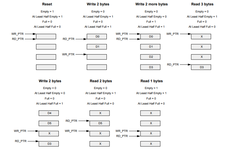
Figure 21-9 FIFO receiver operation.
Fast FIFO mode (FIFO FAST)
When the FIFO operates in the output buffer mode, the FIFO load operation typically uses the clock frequency of the selected Datapath to clock the recording signal. As shown in Figure 21-10, when you select fast FIFO (FIFO FAST) mode for this particular operation, you can select the bus frequency. When used in conjunction with the Level / Edge = Edge mode , this operation reduces the transfer delay from the battery to the FIFO from the Datapath clock period to the bus clock frequency period, since the bus frequency can be much higher. This allows the CPU or DMA to read the resulting FIFO with minimal latency.
As shown in Figure 21-10, the fast boot operation is performed regardless of the current Datapath clocking, but using a bus clock frequency can increase power consumption.
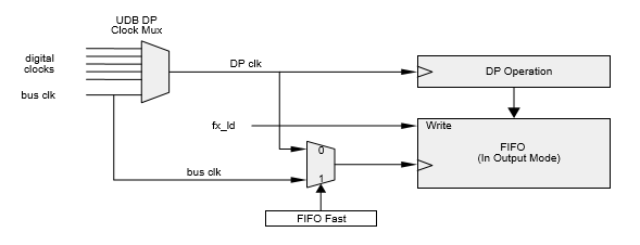
Figure 21-10. Receivers fast configuration FIFO.
Record mode in FIFO Edge / Level (by differential / level)
There are two ways to write to the FIFO from Datapath. In the first mode, data is synchronously transferred from the batteries to the FIFO. The control signal of this record (FX_LD) is usually generated by a state machine or a condition synchronized with the clocking of the Datapath. The FIFO will be recorded in any cycle in which the input load control signal is '1'. In the second mode, the FIFO is used to capture battery values in response to a positive drop in the FX_LD signal. In this mode, the signal format of the signal is arbitrary (however, its period must be equal to at least one Datapath clocking cycle). An example of this mode is to capture the value of a battery using the input of an external leg as a trigger. The limitation of this mode is that
Figure 21-11 shows the implementation of the differential detection mode at the input FX_LD. The mode of both FIFOs in UDB is controlled by the same bit toggling this option. Note that the differential detection is clocked at a frequency equal to the frequency of the selected FIFO.
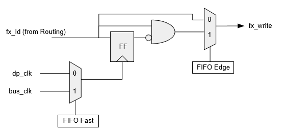
Figure 21-11. Differential detection for internal FIFO recording receivers.
FIFO software capture mode (Software Capture)
A common and important requirement is to ensure that the CPU and DMA reliably read the contents of the battery during normal operation. This is done using software capture and enabled with the FIFO Cap configuration bit. This bit applies to both FIFOs in UDB, but works only when the FIFO is in output buffer mode. When using software capture, F0 must read from A0, and F1 from A1.
As shown in Figure 21-12, reading the battery initiates writing to the FIFO from the battery. The signal is chained together so that reading a specific byte simultaneously captures the battery values of all UDBs in the chain. This allows an 8-bit processor to successfully read 16 bits or more simultaneously. The data returned when reading the battery should be ignored, and the captured value can be immediately available for reading from the FIFO.
The traced FX_LD signal, which generates the FIFO load, is sent to the OR term along with the program capture signal. When hardware and software capture are used at the same time, the result may be unpredictable. As a rule, these functions should be mutually exclusive, but hardware and software capture can be used simultaneously, under the following conditions:
- FIFO capture clocking mode is set to FIFO FAST.
- FIFO recording mode is set to FIFO EDGE.
Under the conditions described above, hardware and software capture work in essentially the same way, and during any bus clock cycle, any of these signals can trigger a capture.
It is also recommended to clear the target FIFO in the program code (ACTL register) before the start of the program capture. Due to this, the pointers to read and write FIFO will be set to a known state.
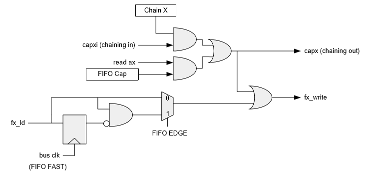
Figure 21-12. Software capture configuration.
Translator's Note:
Frankly, I do not fully understand the full depth of the meaning of this section. Perhaps someone will explain the essence in the comments. But it creates a strong impression that this is primarily intended to enable the 8-bit processor core to have time to read the contents of a battery of higher capacity. Such kernels are used in PSoC-3. As a result, the contents of the battery atomically jumps to the FIFO, after which the contents of the latter can easily be read in 2 or more cycles (in order to pump 16 or 32 bits, plus in the MCS-51, operations will be conducted in separate commands, which will also take cycles). afraid that it will be changed. And for ARM cores, it seems that this is nothing more than an unnecessary rudiment.
FIFO control bits
The Auxiliary Control register, which can be used to control the FIFO during normal operation, contains 4 bits.
The FIFO0 CLR and FIFO1 CLR bits are used to reset or clear the FIFO. When one of these bits is set to '1', the associated FIFO is reset. The bit must be restored to its original value ('0') in order for the FIFO to continue. If the value of the bit remains equal to one, the corresponding FIFO will be disabled and will work as a single-byte buffer with no status. The data can be written to the FIFO, the data is immediately readable and can be overwritten at any time. The direction of the data using the FX INSEL [1: 0] configuration bits can still be set.
The FIFO0 LVL and FIFO1 LVL bits define the level at which the FIFO will trigger the “bus” status bit(when the tire is reading or writing to the FIFO). That is, the status of the “bus” status depends on the given direction, as shown in the table below.
Table 21-5. FIFO Level Control Bits
| FIFO LVL | Input buffer mode (bus writes to FIFO) | Output buffer mode (bus reads from FIFO) |
|---|---|---|
| 0 | Not full. At least 1 byte can be written. | Not empty. At least 1 byte can be read. |
| one | Depleted at least half. At least 2 bytes can be written. | At least half full At least 2 bytes can be read |
Asynchronous FIFO
Figure 21-13 shows the principle of asynchronous operation of the FIFO. As an example, imagine that F0 operates in the input buffer mode, and F1 in the output buffer mode, which is a typical configuration of the TX and RX registers.
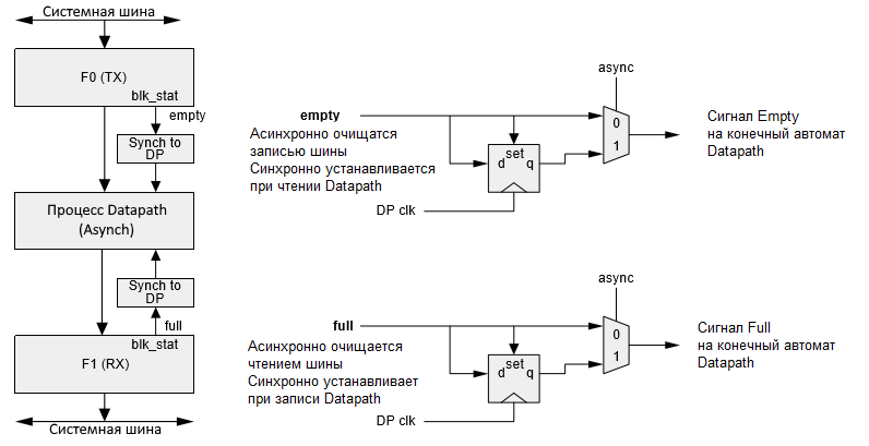
Figure 21-13. Asynchronous FIFO operation.
On the TX side, the Datapath state machine uses the Empty flag to determine if there are any bytes available to receive. The Empty value is set synchronously with the Datapath state machine, and cleared asynchronously due to a write from the bus. After cleaning, the status is synchronized with the Datapath state machine again.
On the RX side, the RX state machine uses Full to determine if there is free space to write to the FIFO. Full valueinstalled synchronously with the Datapath state machine, and cleared asynchronously due to the bus read. After cleaning, the status is synchronized with the Datapath state machine again.
One bit of the FIFO ASYNCH is used to enable this synchronization method, after activation this method is applied to both FIFOs.
It applies only to the Block status , since it is assumed that the Bus status is naturally synchronized by the interrupt process.
Table 21-6. Parameters of synchronization of the Block FIFO status .
| ASYNC | ADD SYNC | Operation | Usage model |
|---|---|---|---|
| 0 | 0 | Synchronized with bus clocking | Changes to the CPU write / read status occur at the bus frequency. Can be used for minimum delay if the Datapatch clocking frequency equal to the bus frequency can be reached . |
| 0 | one | Resync from bus frequency to Datapath frequency. | This mode should be the default mode of operation. When the CPU performs read / write operations, the status change will be resynchronized with the frequency used in the Datapath. Allows you to use the full period of the Datapath frequency to set the signal for the UDB logic. |
| one | 0 | Reserved | - |
| one | one | Dual Bus Clock Frequency to Datapath Frequency. | When the clock pulses for Datapath are not only not synchronized with system clock frequencies, but are also generated by a separate independent generator, this parameter can be used to double- synchronize read and write CPUs with Datapath clocks. |
FIFO overflow during operation
To safely implement internal (Datapath) and external (CPU or DMA) read and write operations, use the FIFO status signals. There is no built-in protection against the conditions of devastation and overflow. If the FIFO is full, and subsequent write operations are performed (overflow), the new data overwrites the beginning of the FIFO (the data that is currently being output is the next in the read queue). If the FIFO is empty, and subsequent read operations are performed (emptying or wasting), the read value is undefined. FIFO pointers retain accuracy regardless of non-completion and overflow.
FIFO clocking invert
Each FIFO has an Fx CK INV control bit, which is responsible for the FIFO clocking polarity. Regarding the clocking polarity of the Datapath. By default, the FIFO works with the same polarity as the Datapath clocking. When this bit is 1, the FIFO operates with reverse polarity relative to the Datapath. This provides support for protocols that exchange data on both fronts, for example, SPI.
Dynamic FIFO Management
Typically, FIFOs are configured statically to either the input buffer mode or the output buffer mode. Alternatively, each FIFO can be configured to operate in a mode in which the direction is controlled dynamically (by external signals). One configuration bit per FIFO (Fx DYN) is responsible for activating this mode. Figure 21-14 shows the configurations available in dynamic FIFO mode.
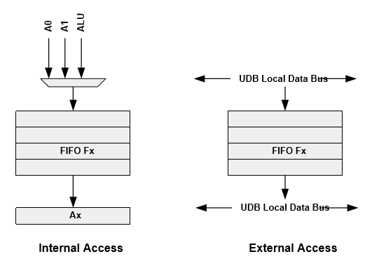
Figure 21-14. Dynamic mode FIFO.
In Internal Access mode, Datapath can read and write to the FIFO. In this configuration, to select the source of write operations in the FIFO, the Fx INSEL bits must be set to 1. Fx INSEL = 0 (CPU bus source) is incorrect in this mode, it can only take values of 1, 2, or 3 (A0, A1, or ALU ). It is worth noting that reading has access only to the corresponding battery, the direction of the data registers in this mode is not available.
In the External Access mode, the CPU or DMA can both read and write to the FIFO.
The configuration dynamically switches between external and internal access using signal forwarding from Datapath. For this, the input signals Datapath d0_load and d1_load are used. It is worth noting that in the dynamic control mode, d0_load and d1_load are not available for normal use when loading registers D0 / D1 from F0 / F1. Dx_load signals can be triggered by any trace signal, including constants.
Consider an example in which, starting from external access (dx_load == 1), a CPU or DMA can write one or more data bytes to a FIFO. Then, when switching to internal access (dx_load == 0), the Datapath can perform operations on the data. After that, when switching to external access, the CPU or DMA can read the result of the calculations.
Since Fx INSEL should always be 01, 10, or 11 (A0, A1, or ALU), which corresponds to the “output buffer mode” during normal operation, the FIFO status signals have the following definitions (depending on the Fx LVL parameter):
Table 21- 7 FIFO status.
| Status signal | Value | Fx LVL = 0 | Fx LVL = 1 |
|---|---|---|---|
| fx_blk_stat | Record Status | FIFO is full | FIFO is full |
| fx_bus_stat | Reading status | FIFO is not full | At least half full |
Since both the Datapath and the CPU can write and read from the FIFO, these signals are no longer considered as “block” and “bus” statuses. The blk_stat signal is used for the write status and the bus_stat signal is for the read status.
21.3.2.3 FIFO Status
There are four FIFO status signals, two for each FIFO: fifo0_bus_stat, fifo0_blk_stat, fifo1_bus_stat and fifo1_blk_stat. The meaning of these signals depends on the direction of the particular FIFO, which is defined by the static configuration. FIFO status is described in detail in Section 21.3.2.2 of the Datapath FIFO .
In the next part we will proceed to the analysis of the Arithmetic Logical Device (ALU).