Multilayer Graphene Superconductor: Study of Flat Zones

Not always, having discovered a substance, scientists immediately understand all of its properties. Improving technologies, including methods, techniques and ways of conducting research, opens up new opportunities for scientists who want to understand what works around us and how. Today we will get to know how researchers have learned that graphene may well have the properties of a superconductor. Superconductivity has been studied since the beginning of the last century, and until now scientists are not aware of all aspects of this physical phenomenon. How exactly did the research team manage to “reconfigure” graphene, what results did the experiments show and what to expect in the future from the research? The scientists' report will help us find answers to these questions. Go.
The basis of the study
For a start, literally in a nutshell, let us remind ourselves what graphene is and what it is eaten with, so to speak.
Graphene, first of all, is a two-dimensional structure consisting of a single layer of carbon atoms. In other words, it is a monolayer of graphite (the main source of graphene).
Graphene has quite unique electrochemical properties, which makes it an ideal candidate for the main role in various studies and as a possible basis for future technologies.
Under laboratory conditions, graphene is obtained in a very complex, time consuming and requiring incredible accuracy method. But in this way you can get the most, so to speak, quality product. The basis of this method is a mechanical effect on highly oriented pyrolytic graphite.
In this study, not monolayer graphene ( MLG ), but two-layer ( BLG ) is used. Since this material has an interesting physical property - the forbidden zone *, which occurs when asymmetry is formed between two layers of graphene.
The forbidden zone * is the range of energy values that an electron cannot have in an ideal crystal. There are 3 main types of solid ones divided by those of the forbidden zone (eV - electron-volt): metals - there is no forbidden zone, semiconductors - up to 3-4 eV and dielectrics - over 4-5 eV.The forbidden zone of two-layer graphene is formed due to the Van Hove singularity.
The main problem of superconductors is that they are such at sufficiently low temperatures. Scientists are trying to raise the temperature limit to room temperature. The researchers cite as an example C 6 CaC 6 , capable of maintaining superconductivity at a temperature of 4 K (-269.15 ° C), and this, as you understand, is far from room temperature.
A possible answer to the question of temperature lies in the combination of two-dimensional graphene with other similar materials. Researchers draw our attention to the BCS theory, which describes the possibility of a bond between electrons with opposite spins and pulses. When exchanging photons, being at the Fermi surface, the electrons begin to attract each other. In this way, electron pairs can be formed, which according to the theory will not interact with single electrons or the lattice, that is, the pairs will move without loss of energy. Thus, the boundary temperature of a superconductor can be increased by increasing the interaction constant (U) or the density of states at the Fermi level n (EF). In graphene and graphite, the density of electron states at the Fermi level is rather low. At the same time there is a direct dependence on the energy level. And here you can apply the theory of flat zones. It is still very difficult to change the value of the interaction constant, the researchers say, but here n (EF) can be increased by means of flat zones.
More details about flat areas are described in this paper .
In the study that we are studying today, the scientists decided to test a new way to “flatten” the electronic zones of graphene and increase the density of electronic states of systems whose very density is very low.
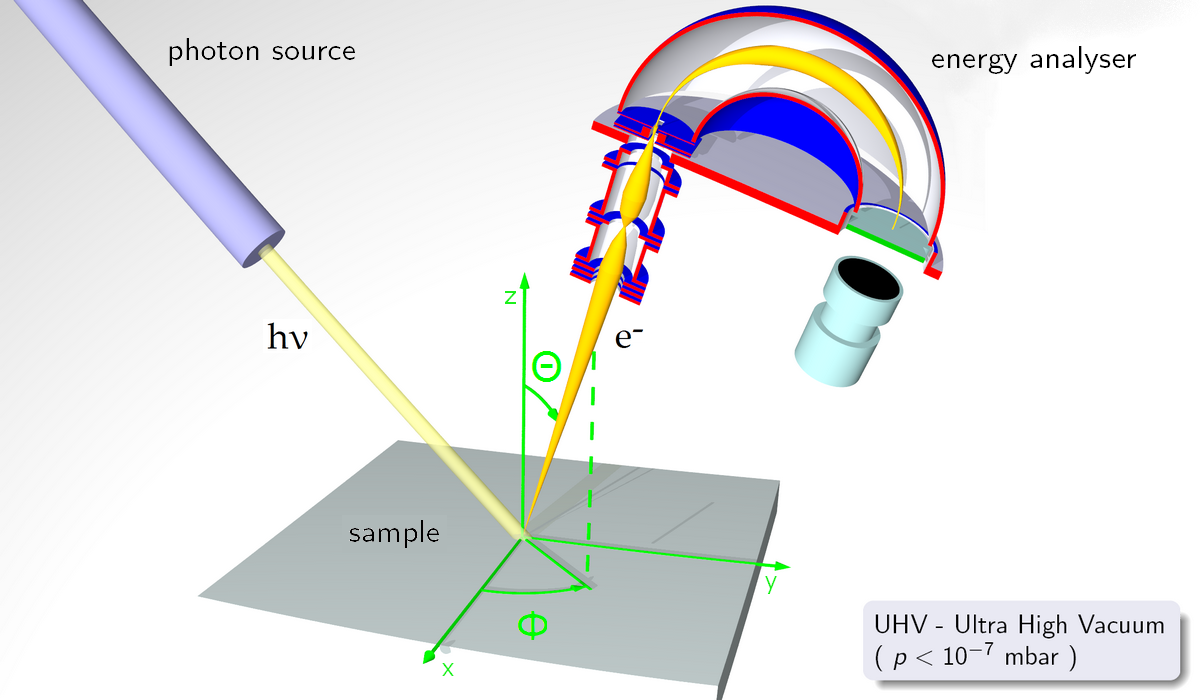
The material basis for the study was a two-layer graphene on silicon carbide (SiC), which, by the way, is a compound of silicon and carbon. Angular-resolution photoelectron spectroscopy (ARPES) has become the data acquisition method.

ARPES installation diagram.
Now let's find out what the researchers did?
Research results

Image No. 1
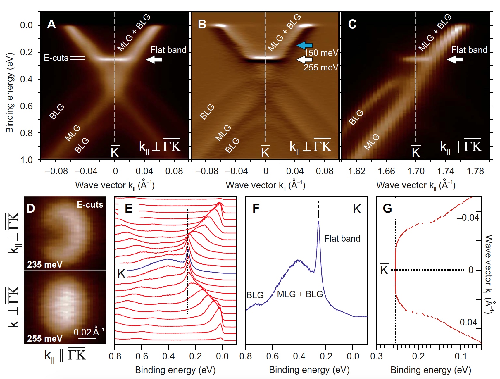
The images above show data collected using ARPES, namely, data from a 6H-SiC sample coated with 1.2 monolayer graphene (MLG).

6H-SiC is one of the polytypes of silicon carbide (the structure with different order of laying layers, that is, the constituent elements are the same, but different types are different).
It was expected that the use of a monolayer would lead to the dominance of the dispersion (Dirac cones) over the weakly intensive two-layer dispersion. However, at the interaction energy level of 255 meV (millielectronvolt), a rather pronounced flat zone is observed. In the image 1a , 1b and 1c, the position of this zone is marked with a white arrow.
The presence of 1.2 monolayer graphene due to the fact that the intensity of BLG photoemission is about 4 times less than that of the MLG zones. The intensity of the flat BLG zone, on the contrary, is 3 times higher than that of the MLG zones. Scientists say that such observations can be found in studies of predecessors, but previously they have not been considered in such detail.
The use of ARPES also made it possible to notice an insignificant flat zone (blue arrow at 1b ), occurring at an interaction energy of 150 meV and a break in the dispersion in the energy range of 150 ... 160 meV.
Next, the researchers decided to analyze the distribution of the intensity of photoemission. For this, a three-dimensional "map" was studied around the sample K point. The analysis showed that only half of the monolayer (Dirac cones) and only half of the dispersion of two-layer graphene are visible, which is associated with the harmful interference from the two graphene sublattices. It can also be seen that the flat zone is evenly distributed on both sides of point K, which is extremely unusual, given the interference of graphene photoemission.
Figure 1d shows two states of the Fermi surface, taken from 1aat an interaction energy of 235 and 255 meV. The difference of 20 meV is very small for ARPES, but it was enough to see significant changes in the Fermi surface. At 235 meV, we see a similarity of the “crescent” due to intensity modulation due to the effect of photoemission interference. But at 255 meV we already see the “disk” without modulation.
Graph 1e (1f for the region around point K) shows how strong the interference of photoemission from the flat zone is. And the graph 1g shows the results of measurements of the dispersion.
Density functional theory
For further analysis, calculations were carried out on the density functional theory over single-layer, two-layer and three-layer graphene.

Image No. 2
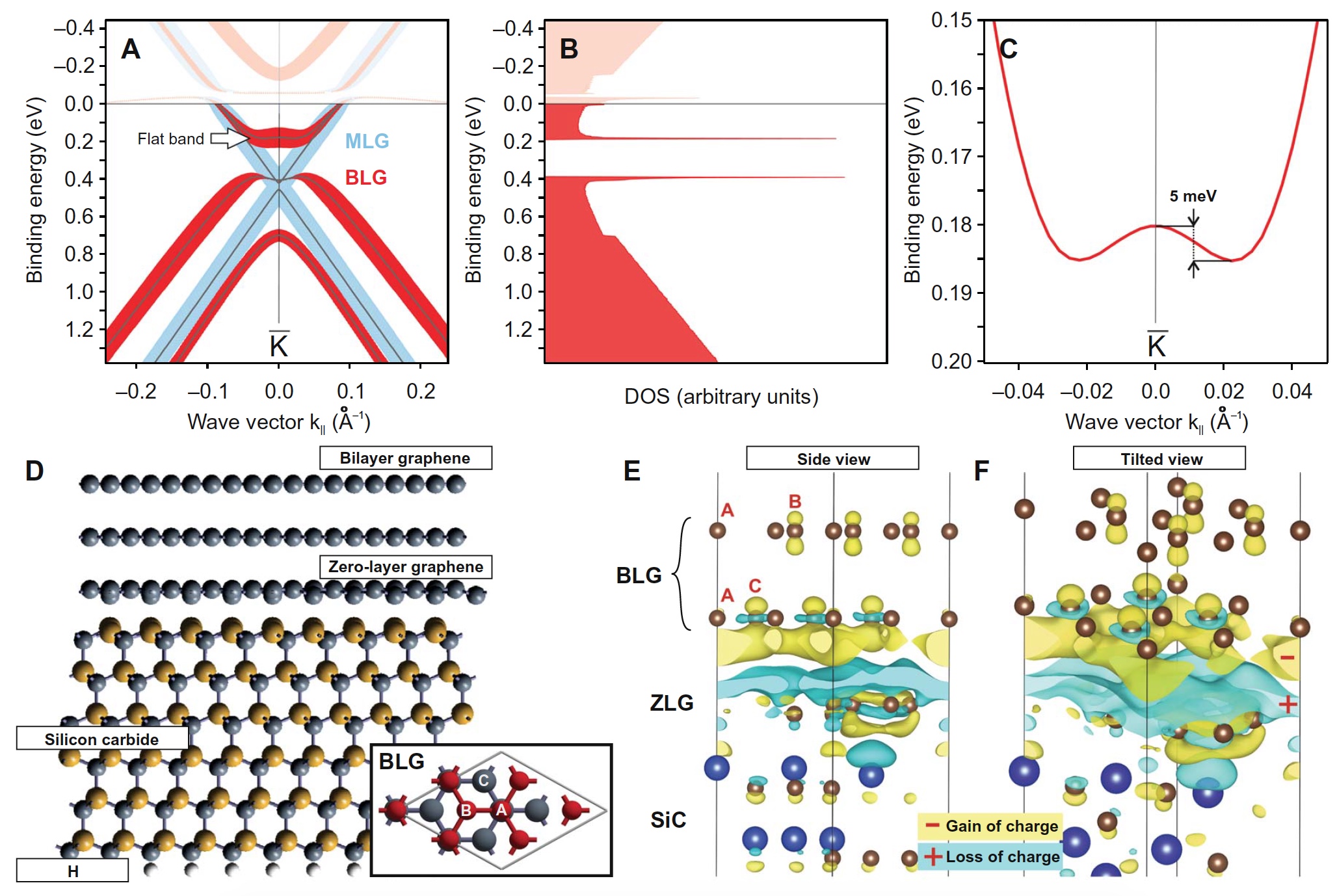
Image 2a shows a comparison of the dispersion calculations for monolayer graphene (blue color) and two-layer (red). The calculated and experimental data on the overall picture of the differences between the monolayer and bilayer structures, as well as the presence of a high level of the density of states ( 2b ), coincide almost perfectly.
An important observation is also the region of origin of the flat zone. As can be seen from image 2aThe flat zone arises not only in the uppermost layer of graphene in the studied two-layer structure, but also in the sublattice as well. A similar effect was also observed when studying the structure of graphene + Ni (111).
Let's go back to schedule 2b again. On it we see two singularities of the density of states at the edges of the layer, between which the gap is clearly visible. Thus, the peaks of the density of states correspond to the Van Hove singularities.
Scientists also deserve a special attention from the SiC substrate, more precisely the question of how strong its influence on the state of two-layer or single-layer graphene is. On images 2e and 2fpresents the results of the check. Isosurfaces are marked in yellow, where there is a process of obtaining a charge, and light blue is a charge loss. Here we see that the sublattices of the upper layer of graphene (A and B) and the sublattice of the lower layer of graphene (A) practically do not react at all, demonstrating only a slight charge asymmetry due to interaction with the SiC substrate. While sublattice C, which is part of the lower layer of graphene, is strongly affected by the interaction between graphene and SiC. In order to better understand what such sublattices in question, pay attention to image 2d , which graphically shows all the layers of the test sample. In the inset at the bottom right, we see how the sublattices A, B, and C are located.
Scientists also analyzed the formation of flat zones in systems with a different order (for example, ferromagnets). As it turned out, in such systems, flat zones also exhibit instability, and superconductivity will prevail over ferromagnetism if the flat zone is sufficiently close to the Fermi level. Such observations can be projected on the current study, as scientists say.
The findings of researchers
First of all, scientists note that although the two-dimensional expansion in the structure relative to the K point is responsible for the high level of photoemission intensity, it is not the main cause of the flat zone. If this expansion had a significant weight in this process, then during the experiments the effects of contraction and amplification of intensity would be visible in other zones of two-layer graphene around point K, but this was not observed.
The disappearance of interference is observed in the flat zone (image 1c), due to which a disk-shaped Fermi surface is formed at an interaction energy of 255 meV. This is a unique phenomenon, especially for graphene. Interference arises due to the localization of the wave function on different graphene sublattices. But in the case of a flat zone, this wave function is localized on only one sublattice, due to which interference disappears.
The appearance of a second flat band was also observed at an interaction energy of 150 meV. However, while scientists can not unambiguously explain the nature of its occurrence. On the one hand, this may be due to the coincidence of the intensity in different regions of the graphene layers. On the other hand, this may be the result of renormalization due to the effects of many bodies, which is often found in monolayer graphene.
The study showed that minor changes in the level of interaction energy can significantly affect the state of the Fermi surface (at 235 meV - the shape of a crescent and at 255 meV - the shape of a disk). In this case, the number of possible scattering channels increases significantly.
It is also important to note that for a detailed study of superconductivity, it is necessary to bring flat zones as close as possible to the Fermi level. Thus, one of the methods can be the introduction of a large number of charge carriers into the graphene layer by intercalating Ca and depositing K. This leads to the formation of a one-dimensional Van Hove singularity.
You can get acquainted with the study in more detail with the help of the report of the researchers and additional materials to it.
Epilogue
Scientists were able to prove that manipulations with sublattices and intermediate layers of the structure of multilayer graphene make it possible to control the shape and characteristics of the flat zone. According to the researchers, the use of this skill in conjunction with the method of enhanced electron-phonon bonds will help in the future to obtain superconductors, whose properties will be maintained at much higher temperatures than now.
Superconductors are of great importance. Already, they are used in many technologies, ranging from superconducting quantum interferometers to MRI scanners. Further study of superconductors, their properties, methods of obtaining them and improving their qualities will not only improve the modern world, but also make it a bit more futuristic.
Thank you for staying with us. Do you like our articles? Want to see more interesting materials? Support us by placing an order or recommending to friends, 30% discount for Habr's users on a unique analogue of the entry-level servers that we invented for you: The whole truth about VPS (KVM) E5-2650 v4 (6 Cores) 10GB DDR4 240GB SSD 1Gbps from $ 20 or how to share the server? (Options are available with RAID1 and RAID10, up to 24 cores and up to 40GB DDR4).
VPS (KVM) E5-2650 v4 (6 Cores) 10GB DDR4 240GB SSD 1Gbps until December for free if you pay for a period of six months, you can order here .
Dell R730xd 2 times cheaper? Only we have 2 x Intel Dodeca-Core Xeon E5-2650v4 128GB DDR4 6x480GB SSD 1Gbps 100 TV from $ 249in the Netherlands and the USA! Read about How to build an infrastructure building. class c using servers Dell R730xd E5-2650 v4 worth 9000 euros for a penny?
