Control of RGB LEDs through the UDB unit of PSoC microcontrollers by Cypress
Introduction
I have long wanted to learn the method of programming UDB blocks in Cypress PSoC controllers, but all hands somehow did not reach. And so, there was a problem in which this could be done. Understanding the materials from the network, I realized that practical recommendations for working with UDB are limited to those or other variations of counters and PWMs. All authors for some reason make their own variations of these two canonical examples, so the description of something else may well be interesting to readers.
So. There was a problem to dynamically control a long line of R28 LEDs WS2812B. Classical approaches to this case are known. You can take the banal Arduino, but there the output goes programmatically, so while the data is being output - everything else is idle, otherwise the time diagrams will fail. You can take STM32 and output data either via DMA to PWM or via DMA to SPI. Techniques are known. I even, at one time, personally through SPI already ruled a line of sixteen diodes. But the overhead is great. One bit of data in the LEDs takes 8 bits in memory for the case of PWM and from 3 to 4 bits (depending on the PLL rate in the controller) for SPI. While there are few LEDs, it is not scary, but if, say, a couple of hundred, then 200 * 24 = 4800 bits = 600 bytes of useful data should be physically stored in a buffer, volume of more than 4 kilobytes for the PWM version or more than 2 kilobytes for the SPI option. For dynamic indication, there should be several buffers, while the STM32F103 has RAM for everything about 20 kilobytes. It’s not that we have rested against an unrealizable task, but the reason for checking whether it can be implemented on PSoC without the need for spending extra RAM is quite significant.
References to the theory
First, let's figure out what kind of a beast is such a UDB and how to work with it. This will help great educational films from the manufacturer of controllers.
Start watching from here , and then at the end of each video will be a link to the next series. Step by step, you will gain basic knowledge and consider the canonical example of “counter”. Well, the control system of traffic lights.
Approximately the same, but chopped into small pieces, can be viewed here . My video did not play, but it can be downloaded and viewed locally. Among other things, there is a canonical example of the implementation of PWM.
Search for ready-made solutions
In order not to reinvent the wheel (and vice versa - to study the technique on someone else's experience), I rummaged around the network in search of ready-made solutions for controlling RGB LEDs. The most popular solution is StripLightLib.cylib. But he has for many years been planning to add support for DMA. And I want to try exactly the solution that does not depend on the CPU. I want to start the process and forget about it, focusing on the preparation of the next frame.
The solution that matches my desires was found at https://github.com/PolyVinalDistillate/PSoC_DMA_NeoPixel .
There everything is implemented on UDB (after all, LEDs are just an excuse, the goal is to study UDB). There is support for DMA. And the project there is clearly beautifully organized.
Problems of the chosen solution
How is the "firmware" in the project PSoC_DMA_NeoPixel, anyone can see after reading the article. This will fix the material. So far, I will only say that at first I simplified the logic of the original firmware without reducing the resources consumed (but it became easier to understand). Then he began to experiment with replacing the logic of the automaton, which promised a gain in resources, but ran into a serious problem. And so it was decided - it is not eliminated! And they began to torment me with vague doubts, does the English author have the same problem? His demo flashes LEDs very nicely. But what if we replace the beautiful filling with “all units” and control the output with an oscilloscope, not with our eyes?
So, as rudely as possible (one can even say “brutal”) we generate data:
memset (pPixelArray,0xff,sizeof(pPixelArray));
        //Call NeoPixel update function (non blocking) to trigger DMA pixel update
        NP_Update();
And we observe this picture on an oscilloscope:
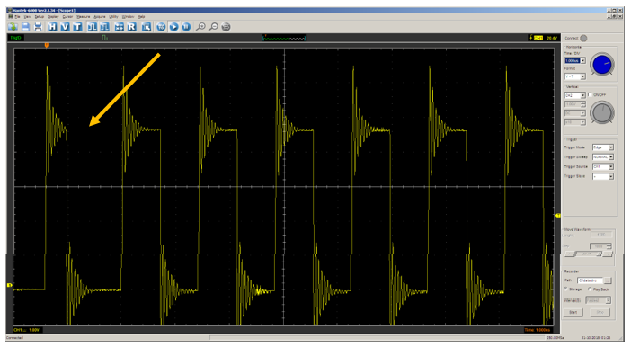
At the first bit, the width is different from all the others. I asked to send all the units, but not all go. Zero was among them! We change the scan:
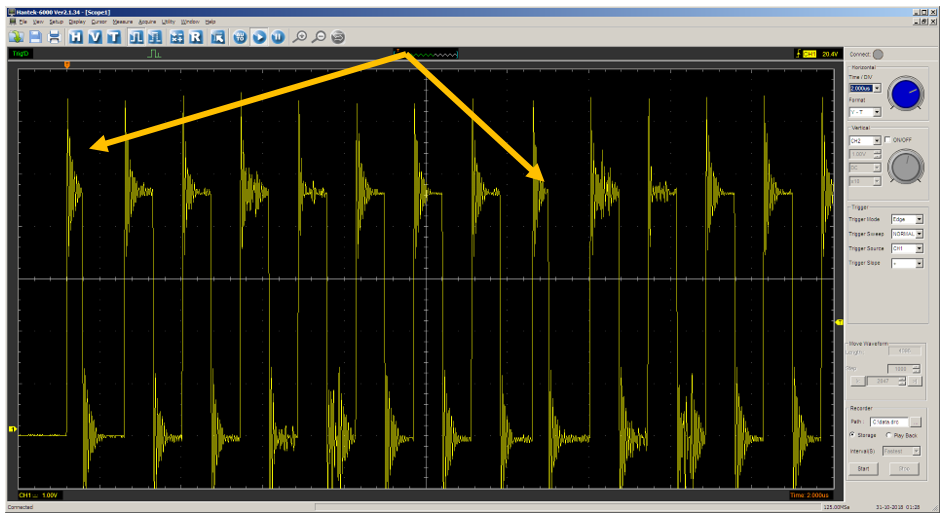
The width is different for every eighth bit.
In general, this example as an independent solution is not suitable, but as a source of inspiration - just perfect. Firstly, its inoperability is not visible to the eye (the LEDs light up brightly anyway, the eye does not see that they shine to half the maximum), but the code is well structured, it is pleasant to take it as a basis. Secondly, this example provides space for finding ways to simplify, and thirdly, it makes you think about how to eliminate the defect. The most is to comprehend the materiel! So once again I recommend, after reading the article, try to disassemble the original example, having understood how it works.
Practical part
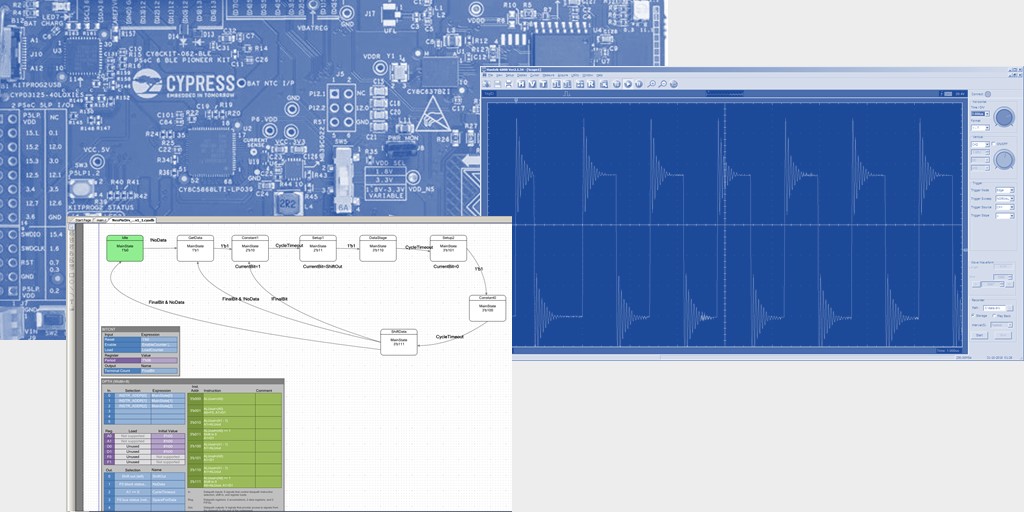
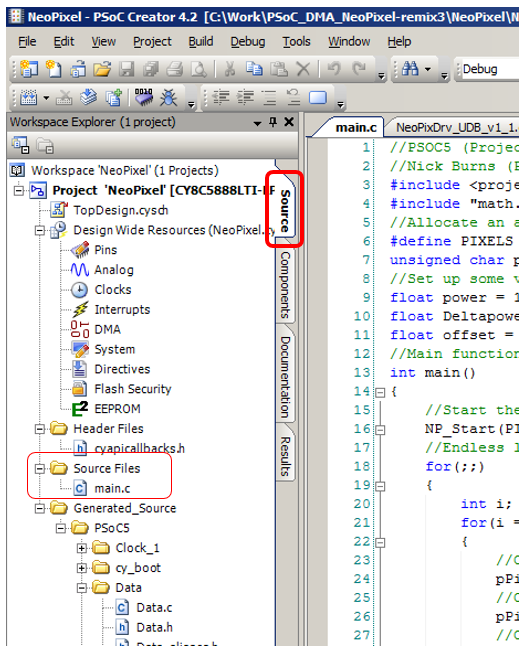
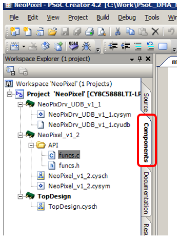
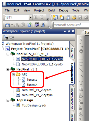
Now we begin to practice. We touch upon the main aspects of UDB firmware development. Consider the relationship and the basic techniques. To do this, open my version of the project . The left block stores information about the working files. By default, the Source tab is open . The main source of the project is the main.c file . Actually, there are no other work files in the Source Files group .
The generated source group contains library functions. It is better not to rule them. After each change in the UDB firmware, this group will be re-generated. So, where in this idyll is a description of the code for UDB? To see it, you need to switch to the Components tab :
The author of the original project made a two-level set of components. At the top level is the NeoPixel_v1_2.cysch scheme . This can be seen from the main scheme:
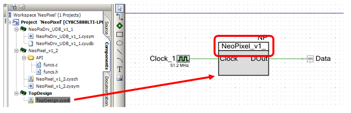
The component looks as follows:
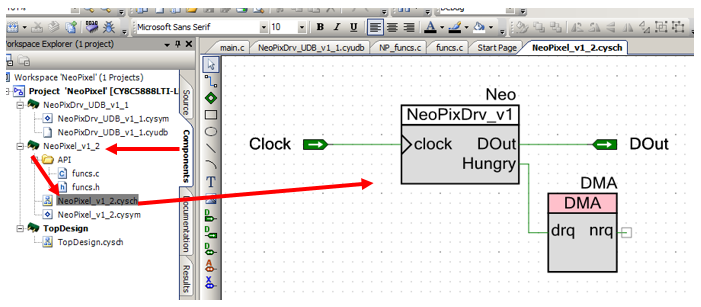
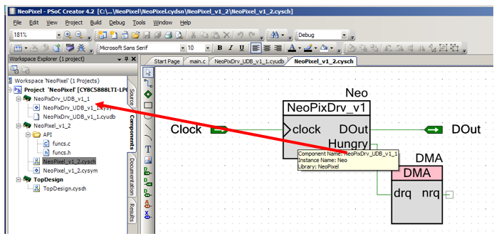
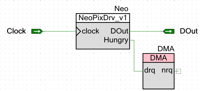
We will consider software support for this scheme later. In the meantime, we find out that the DMA block is located on it and a certain NeoPixDrv_v1 symbol . This mysterious block is described above in the tree, which follows from the following tooltip:
UDB Firmware
Open that component (file with the extension .cyudb ). The opened drawing is simply huge. We begin to understand what is what.
Unlike the author of the original project, I consider the transfer of each bit of data in the form of three equally-sized (in time) parts:
- Starting part (always 1)
- Part of the data
- Stop part (always 0)
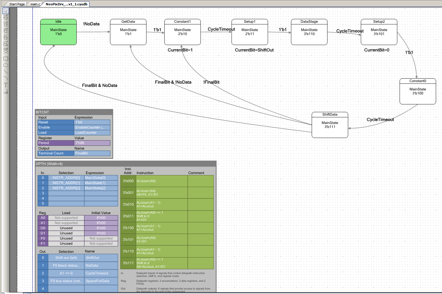
With this approach, a large number of counters are not required (in the original, there were as many as three, which consumed a large amount of resources). The length of all parts is the same and can be set using one register. Thus, the transition graph firmware machine comprises the following states:
Idle state ( Idle ). It remains in the machine until new data has arrived in the FIFO.
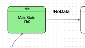
From the training videos I was not entirely clear how the states of the machine are connected with the ALU. The authors use the connection as something self-evident, but I, as a beginner, could not immediately see it. Let's immediately understand in detail. The figure above shows that the state of Idleencoded by the value 1'b0. It will be more correct to 3'b000, but the editor will still redo everything. The inputs of the Datapath block are described like this:
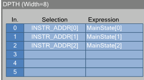
If you double-click on them, a more detailed option will appear:
This means that the zero bit of the address of the ALU instruction address corresponds to the zero bit of the variable specifying the state of the machine. The first is the first, the second is the second. If desired, the bits of the address of the ALU instruction can be matched by any variables and even expressions (in the original version, the second bit of the address of the instruction of the ALU was matched exactly by the expression, and in the current version it is clearly not used, but as an outgoing brain the example is very clear, then you can look).
So. With the current setting of the inputs, which is the binary status code of the automaton, such an ALU instruction is used. When we are in the Idle state , which has the code 000, the null instruction is used. Here it is:

I already know from this record that this is a banal NOP. But you can double click on it and read the full version:
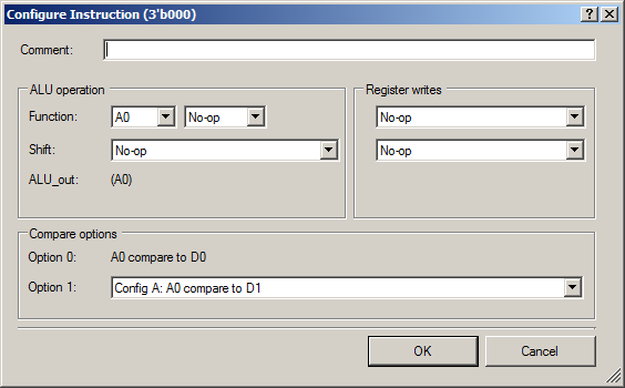
NOPs are written everywhere. Registers are not filled with anything.
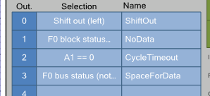
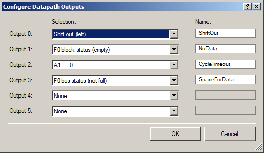
Now let's see what this mysterious flag is ! NoData , forcing the machine gun to leave the state of rest. This is the output from the Datapath block . You can describe up to six outputs. Just datapathIt can generate many more flags, but there are not enough tracing resources at all, so you need to choose which six (or less) we really need. Here is the list in the figure:
If you double-click on it, the details will be revealed:
Here is the full list of flags that could be displayed:
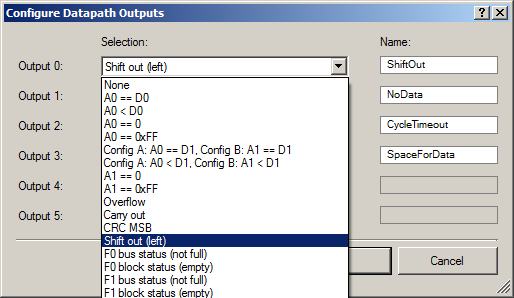
Select the desired flag, you should give it a name. From this point on, the system has a flag. As you can see, the NoData flag is the name for the F0 block status (empty) chain . That is a sign that there is no data in the input buffer. Ah ! NoData, accordingly, its inversion. Sign of data availability. As soon as the data gets into the FIFO (programmatically or with the help of DMA), the flag will be cleared (and its inversion set), and on the next clock the machine will exit the rest state and go to the GetData state .
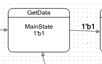
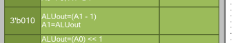
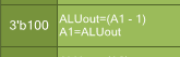
As you can see, the machine will definitely come out of this state, having stayed in it for exactly one cycle. No actions are indicated for this state on the transition graph. But you always have to look at what the ALU will do. The status code is 1'b1, that is, 3'b001. We look at the corresponding address in the ALU:
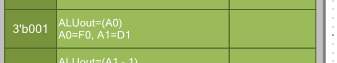
There is something. Having no experience reading what is written here, we reveal it by double clicking on the corresponding cell:
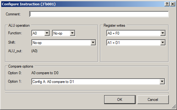
It follows that the ALU itself still does not perform any actions. But in the register A0 will be placed the contents of FIFO0, that is, the data coming from the program or the DMA block. Looking ahead, I will say that A0 is used as a shift register, from which the byte will be output in a sequential form. Register A1 will put the value of register D1. In general, all registers D are usually filled with software before the active operation of the equipment. Then, when considering the API, we will see that the number of machine ticks, which sets the duration of a third bit, is put in this register. So. The shifted value has fallen into A0, and the value of the duration of the starting part of the bit in A1. And in the next cycle, the machine will certainly switch to the Constant1 state .
As follows from the name of the state, the constant 1 is generated here. Let's consider the documentation on the LED. This is how the unit should be transmitted:
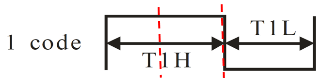
And here it is - zero:
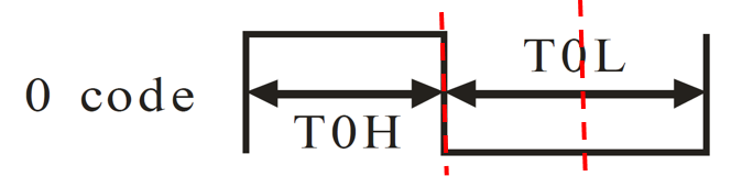
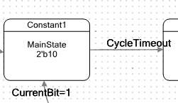
I added the red lines. If we assume that the duration of the third is equal, then the requirements for the duration of the pulses (given in the same documentation) are fulfilled. That is, any impulse consists of a starting unit, a data bit and a stop zero. Actually, the starting unit is transmitted when the machine is in the Constant1 state .
In this state, the machine clicks the unit in its internal trigger. Trigger Name CurrentBit. In the original project, it was generally a trigger that sets the state of the auxiliary machine. I decided that that machine would only confuse everyone, so I just started the trigger. It is not described anywhere. But if you enter the properties of the state, the following entry is visible in the table:
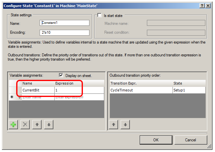
And under the state on the graph there is the following text:
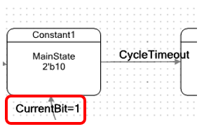
Do not be afraid of the “Equal” symbol. These are features of the editor. In the resulting Verilog code (automatically created by the same system) there will be an arrow:
Constant1 :
        begin
            CurrentBit <= (1);
            if (( CycleTimeout ) == 1'b1)
            begin
                MainState <= Setup1 ;
            end
        end
The value snapped in this trigger is the output signal of our entire unit:
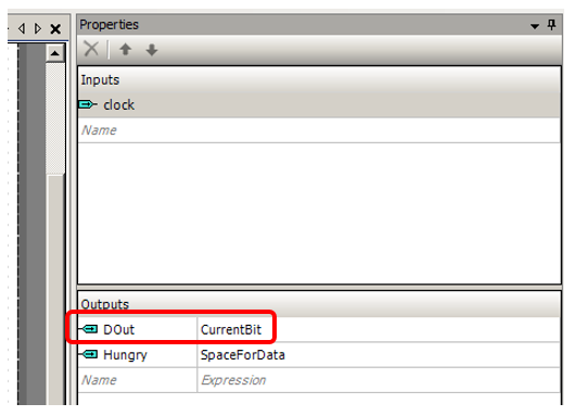
That is, when the machine enters the Constant1 state , a unit will hit the output of the unit we are developing. Now we look at how the ALU is programmed for the address 3'b010: Expand
this element: One
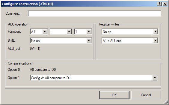
is subtracted from register A1. The output value of the ALU falls into register A1. Above, we considered that A1 is a clock counter used to set the duration of the output pulse. Let me remind you that it was loaded from D1 at the last step.
What is the condition out of the state? CycleTimeOut . It is described among the exits as follows:
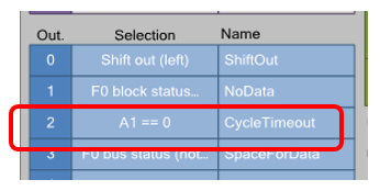
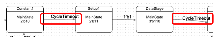
So, we bring the logic together. In the past state, the contents of the D1 register previously filled with the program fell into the A1 register. At this step, the machine translates the CurrentBit trigger to one, and in the ALU, register A1 decreases on each clock cycle. When A1 becomes equal to zero, the flag will be automatically coded, to which the author gave the name CycleTimeout , as a result of which the machine will go to the state Setup1 .
The state Setup1 prepares data for transmitting a useful pulse.
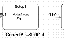
We look at the instructions of the ALU at 3'b011. I will immediately open it:
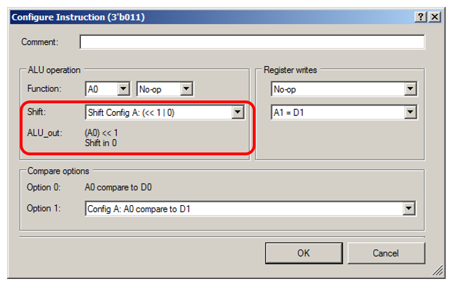
It would seem that the ALU has no action. Operation same nop. And the output of the ALU does not go anywhere. But it is not. An extremely important action is the shift of data in the ALU. The fact is that the carry bit among the outputs is connected to our ShiftOut circuit :

And as a result of this shift operation, the shifted value itself will not get anywhere, but the ShiftOut circuit will take the value of the high bit of the A0 register. That is, the data that should be transmitted. Under the state of the graph, it is clear that this value, which has been output from the ALU to the ShiftOut circuit , will be latched into the CurrentBit trigger . Let me show the picture again so as not to wind up the article:
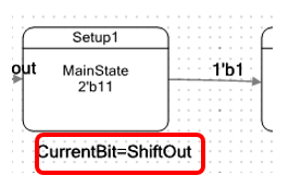
The transmission of the second part of the bit, the immediate value 0 or 1, begins.
We return to the instructions for the ALU. In addition to what has already been said, it is clear that along the way, the contents of register D1 will again be put in register A1, so that the second third of the pulse can be measured again.
The DataStage state is very similar to the Constant1 state . The machine simply subtracts the unit from A1 and goes to the next state when it reaches zero. Let me even show it like this:
like this:
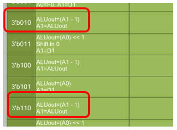
Then comes the state of Setup2 , the essence of which we already know.
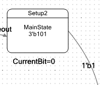
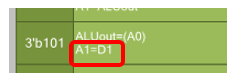
In this state, the CurrentBit triggeris reset to zero (since the third third of the pulse will be transmitted, the stop part, but it is always zero). ALU loads the contents of D1 into A1. You can even see it in a brief eye with a pointed eye:
The Constant0 state is completely identical to the Constant1 and DataStage states . Subtract a unit from A1. When the value reaches zero, we exit the state ShiftData : The
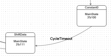
state ShiftData is more complex. In the corresponding instructions for the ALU, the following actions are performed: The
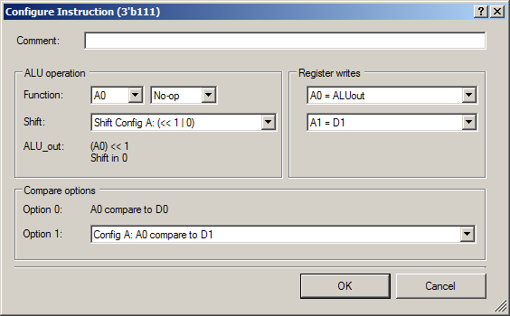
register A0 is shifted by 1 bit, and the results are placed back into A0. In A1, the content of D1 is put again to begin measuring the starting third for the next bit of data.
Output arrows should be considered with regard to priorities, for which we double-click on the state of ShiftData .
If not the last bit is transmitted (how this flag is formed, just below), then we transfer one for the next bit of the current byte.
If the last bit is transmitted and there is no data in the FIFO, we go to a state of rest.
Finally, if the last bit is transmitted, but there is data in the FIFO, we go to sample and transmit the next byte.
Now about the bit counter. There are only two batteries in the ALU: A0 and A1. They are already occupied by the shift register and the delay counter, respectively. Therefore, the bit counter is used external.
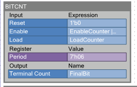
Double-click on it:

The value at boot is six. It is loaded on the LoadCounter flag .described in the variables section:
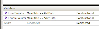
That is, when the next data byte is taken, this constant is loaded in parallel.
When an automaton enters the ShiftData state , the counter decreases the value. When the value reaches zero, the TerminalCount output connected to the FinalBit circuit of our family is set . It is this circuit that determines whether the automaton will send the next bit of the current byte or transmit a new byte (well, or wait for a new data packet).
Actually, from logic - everything. How the SpaceForData signal is generated , which sets the state of the Hungry output (informing the DMA block that the next data can be transmitted), readers are invited to track themselves.
Software support
The author of the original project chose to make software support for the entire system in a block describing a complex solution. Let me remind you that we are talking about this block:
From this level there is a management of both the DMA library block and all parts included in the UDB part. To implement the API, the original author added header and program files:
The format of the body of these files is depressing. All because of the love of the developers PSoC Designer to "pure sam." Hence the terrible macros and kilometer names. Class organization in C ++ would be most welcome here. At least, we checked it when implementing our RTOS MAX: it turned out nice and comfortable. But here you can talk a lot, and you will have to use what is lowered from above. I will only briefly show how the API function looks like, containing these same macros:
volatilevoid* `$INSTANCE_NAME`_Start(unsignedint nNumberOfNeopixels, void* pBuffer, double fSpeedMHz)
{
    //work out cycles required at specified clock speed...
    `$INSTANCE_NAME`_g_pFrameBuffer = NULL;
    if((0.3/(1.0/(fSpeedMHz))) > 255) returnNULL;
    unsignedchar fCyclesOn = (unsignedchar)(0.35/(1.0/(fSpeedMHz)));
    `$INSTANCE_NAME`_g_nFrameBufferSize = nNumberOfNeopixels*3;
    //Configure for 19.2 MHz operation
    `$INSTANCE_NAME`_Neo_BITCNT_Start();        //Counts bits in a byte//Sets bitrate frequency in number of clocks. Must be larger than largest of above two counter periods
    CY_SET_REG8(`$INSTANCE_NAME`_Neo_DPTH_D1_PTR, fCyclesOn+1);
    //Setup a DMA channel
    `$INSTANCE_NAME`_g_nDMA_Chan = `$INSTANCE_NAME`_DMA_DmaInitialize(`$INSTANCE_NAME`_DMA_BYTES_PER_BURST,
`$INSTANCE_NAME`_DMA_REQUEST_PER_BURST,
HI16(`$INSTANCE_NAME`_DMA_SRC_BASE),
HI16(`$INSTANCE_NAME`_DMA_DST_BASE));
    if(pBuffer == NULL)
...
These rules of the game will have to accept. Now you know where you can take inspiration from when developing your functions (best of all, in the original project). And I would prefer to talk about the details, taking the variant already processed by the generator.
After generating the code (described below), this file will be stored here:
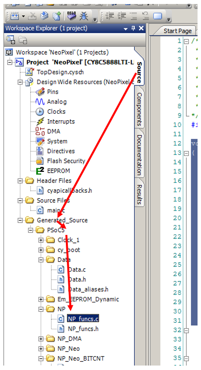
And the view will already be perfectly readable. There are two functions so far. The first initializes the system, the second starts the transfer of data from the buffer to the line of LEDs.
Initialization affects all parts of the system. There is an initialization of the seven-bit counter included in the UDB system:
NP_Neo_BITCNT_Start(); //Counts bits in a byteThere is a calculation of the constant, which should be loaded into the D1 register (I remind you that it sets the duration of each of the third bits):
unsignedchar fCyclesOn = (unsignedchar)(0.35/(1.0/(fSpeedMHz)));
    CY_SET_REG8(NP_Neo_DPTH_D1_PTR, fCyclesOn+1);
Setting up a DMA block takes up most of this function. The source is a buffer, and the receiver is the FIFO0 of the UDB block (in kilometer records, NP_Neo_DPTH_F0_PTR ). The author of this setting was in the data transfer function. But, in my opinion, doing all the calculations for the sake of each transmission is too wasteful. Especially if one considers that one of the actions inside the function looks very, very voluminous.
//work out cycles required at specified clock speed...
    NP_g_pFrameBuffer = NULL;
    NP_g_nFrameBufferSize = nNumberOfNeopixels*3;
    //Setup a DMA channel
    NP_g_nDMA_Chan = NP_DMA_DmaInitialize(NP_DMA_BYTES_PER_BURST,
NP_DMA_REQUEST_PER_BURST, HI16(NP_DMA_SRC_BASE), HI16(NP_DMA_DST_BASE));
	...
    NP_g_nDMA_TD = CyDmaTdAllocate();
    CyDmaTdSetConfiguration(NP_g_nDMA_TD, NP_g_nFrameBufferSize, CY_DMA_DISABLE_TD, TD_INC_SRC_ADR | TD_AUTO_EXEC_NEXT);
    CyDmaTdSetAddress(NP_g_nDMA_TD, LO16((uint32)NP_g_pFrameBuffer), LO16((uint32)NP_Neo_DPTH_F0_PTR));
    CyDmaChSetInitialTd(NP_g_nDMA_Chan, NP_g_nDMA_TD);
The second function on the background of the first is the height of laconicism. Just the first is called at the initialization stage, when the speed requirements are quite free. While working, it is better not to waste processor cycles on anything extra:
voidNP_Update(){
    if(NP_g_pFrameBuffer)
    {
        CyDmaChEnable(NP_g_nDMA_Chan, 1);
    }
}
There is clearly not enough functionality for working with multiple buffers (to provide double buffering), but in general, the discussion of API functionality is beyond the scope of the article. Now the main thing is to show how to add software support to the developed firmware. Now we know how to do it.
Project generation
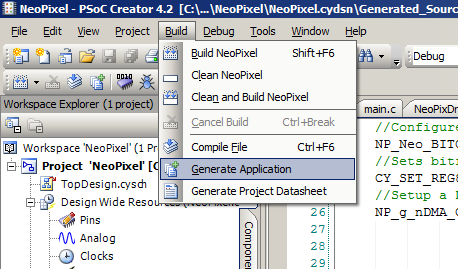
So, the entire firmware part is ready, the API is added, what to do next? Select the menu item Build-> Generate Application .
If everything goes well, you can open the Results tab and view the file with the rpt extension .
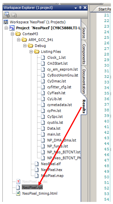
It shows how much system resources are spent on the implementation of the firmware part.
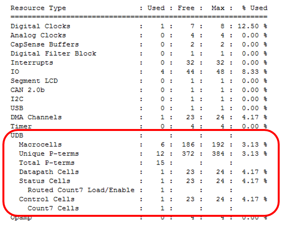
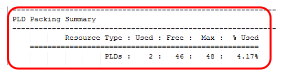
When I compare the results with those that were in the original project, it gets warmer in my heart.
Now go to the Source tab and start working with the software part. But this is already trivial and does not require special explanations.

Conclusion
Hopefully, from this example, readers learned something new and interesting about practical work with UDB blocks. I tried to focus on both the specific task (LED control) and the design methodology, since I had to comprehend some aspects that were obvious to specialists. I tried to mark them while the memories of the search were fresh. As for the solved problem, the time diagrams I got were not as perfect as the author of the original design, but they fit perfectly into the tolerances defined in the documentation for the LEDs, and the system resources were significantly less.
In fact, this is only a part of the non-standard information found. In particular, from most materials it may seem that UDB works well only with serial data, but it is not. Found Application Note, which briefly shows how you can drive and parallel data. It would be possible to consider specific examples based on this information (although, to overshadow the FX2LP, another controller from Cypress, will not succeed: PSoC has a lower USB bus speed).
I have ideas in my head about how to solve the “firmware” problem of a 3D printer that has tormented me for a long time. There, interrupts serving stepper motors, devouring just an insane percentage of processor time. In general, I talked a lot about interruptions and processor time in the article about the MAX RTOS. There are estimates that for servicing stepper motors, it is possible to take out all the shelters completely at the mercy of UDB, leaving the processor with a purely computational task without fear that it will not have time to do this in a dedicated time slot.
But it will be possible to speculate about these things only if the topic turns out to be interesting.