Custom floating point format on FPGA
Hello!
This article will focus on floating point numbers and, in particular, on the implementation of the specialized FP23 format on programmable logic integrated circuits (FPGAs). As part of a specific project, I had the idea to implement a floating-point data format that is optimal for certain needs. As a result, this idea turned into a real project, which subsequently found application in some interesting tasks of digital signal processing. The article discusses the main difficulties in implementing the floating point data format on the Xilinx FPGA, and considers the basic mathematical operations in the FP23 format. Also at the end of the article you can find the source code of the project, which can be freely used in your tasks or based on it to implement similar data formats.
Floating-point numbers are actively used in modern signal processors, video cards, and even in FPGAs. In accordance with the IEEE 754 standard , they are represented as a combination of exponent (exponent), mantissa and sign. Numbers in the IEEE 754 standard have 32 bits ( float ). For the sake of clarity, writing numbers in a float is written in normal form or reduced to a normalized form after mathematical operations and transformations on numbers. The range of possible values depends on the number of bits of the mantissa and exponent. Float is characterized by fixed relative accuracy and variable absolute accuracy. Main advantages and disadvantages of numbers in float format:
For modern FPGA chips, the implementation of floating-point numbers is not difficult. For leading manufacturers - Xilinx and Altera, there are ready-made SOFT IP cores that implement float according to the standard. For Altera, the latest families have HARD IP cores that implement the IEEE 754 format on DSP blocks.
The main element base for performing mathematical operations and tasks of digital signal processing is advanced FPGA families. The work is carried out on the FPGA company Xilinx, which contain blocks of vectors of configurable cells. First of all, these are universal blocks of digital processing and mathematics - DSP48E1 (for FPGAs of the Virtex-6 series and 7 families) and DSP48E2 (for FPGAs of the UltraScale family). These blocks allow you to perform the functions of addition and subtraction of numbers, shift and transfer, high-speed multiplication, accumulation multiplication (MACC), checksum search, etc. On DSP48 cells in modern FPGAs, many tasks are performed - the development of CIC and FIR filters, high-speed calculation of FFT / IFFT, the implementation of digital frequency synthesizers (DDS and CORDIC), the creation of various formats for presenting data and a set of operations for them.
The second basic component of FPGAs is block memory. For Xilinx FPGAs, these are RAMB36E1 (or RAMB18E1) cells. These are two-port memory elements implemented inside crystals in the form of columns of identical blocks. The number of columns of internal memory depends on the size of the chip. The maximum capacity of a memory block is 36Kbit, while it can be configured as two independent blocks of 18Kbit each. The memory can be used with a data width of 1 to 72 bits. In the absence of free resources of FPGA block memory, you can use distributed memory in special SLICEM cells. For Ultrascale FPGAs, the amount of such memory is up to 512x1, with the possibility of reconfiguring the depth and bit depth of the bus.
Given the above features for the implementation of the analog and digital parts, the task is formed as follows. Let the bit capacity of the data entering the FPGA chip with ADC chips be 16 bits. As the FPGA selected the smallest chip Kintex-7. The task is to translate the 16-bit signed integer FIX16 into a specialized floating-point format FP23 and vice versa, while ensuring maximum processing speed inside the FPGA with minimal expenditure of crystal resources . In addition, it is necessary to designate and implement a set of basic mathematical operations - addition, subtraction and multiplication.
FP23 is a special format for representing floating point numbers. Unlike the IEEE 754 standard, the word length in FP23 format is not 32 bits, but only 23 bits. The following formula is a simplified representation of the number reflects the «A» in FP format:

Mantissa ( mantissa) in FP23 format is a 17-bit positive number. It is always displayed in a normalized form as a result of all transformations, i.e. the most significant bit of the mantissa is always “1”. To save crystal resources and simplify writing, the 17th bit of the mantissa is never displayed in the packed resulting 23-bit word (see the figure). Therefore, when calculating mathematical operations and translating from one format to another, it is necessary to remember that the mantissa is normalized, and the value 216 must be added to the 16-bit non-zero number. The exponent or exponent in the FP23 format is a 6-bit positive number that determines how much is the mantissa multiplied. Under the sign ( sign) the remaining one bit is highlighted, with a zero value of the bit corresponding to positive numbers, and a single value determining negative numbers. Thus, the number A in FP23 format is described by three bit fields: “exponent” (EXP (A)) , “sign” (SIGN (A)) and “mantissa” (MAN (A)) .

Table 1 shows the bit depth of the data, the range of possible values of the mantissa and exponent, etc.

So, the first step in developing a floating-point data format on an FPGA is to convert a signed fixed-digit integer to the FP23 floating-point format, while ensuring maximum processing speed inside the FPGA. The second step is the inverse conversion of numbers from the FP23 format to a fixed-point format with the ability to scale the output to a specific division factor. And finally, at the third stage, to fully utilize the full power of the FP23 format, it is necessary to implement mathematical operations - addition, subtraction and multiplication.
Before describing the FP23 modules, it is necessary to answer the natural question: “Why is the data capacity in the format exactly 23 bits?” The answer consists of several components. Firstly, one bit is used for the character and the 15 remaining bits for the integer part, so the mantissa and character occupy at least 16 bits. For an exponent, taking into account the offset in the formula, a minimum of 5 bits is required. The more bits are allocated to the exponent, the larger the result (the range of possible values is expanded). Let the exponent have 6 digits, and the mantissa is represented as a 16-bit number, 1 digit is assigned to the sign. Then, to represent numbers in the FP23 format, exactly 23 bits are used. If you use the hidden bit of the mantissa, which is equal to 1 for non-zero values and equal to 0 for zero values of a binary number, then the bit capacity is 24.
In addition, the value "23" was not chosen randomly, because in the future, FPGA memory is required to store the vector of complex values. A pair of values without displaying a hidden bit has a total capacity of 46, with a hidden bit of 48, which fits exactly three RAMB18E1 memory blocks in width. Also, for a pair of values, you can use the additional functions of the DSP48E1 ¬ block — quick comparison of two numbers, parity, and quick summation in SIMD mode.
To convert data from the integer character type FIX16 to the FP23 format, it is necessary to use the FPGA chip logic and the built-in DSP48E1 multipliers. The figure shows a block diagram of the conversion of data into the FP23 format.
The maximum bit depths of the DSP48E1 block factors are 25 and 18, respectively, where the most significant bit is significant. To multiply numbers without regard to the sign in the DSP48E1 module, the effective bit depth of the input data is reduced by 1 bit. The converter does not use RAMB18E1 block memory.
Accordingly, in order to find the sign of a number, it is necessary to take the most significant (signed) bit of the input data. The search algorithm for the mantissa MAN (A) based on the FPGA primitives is as follows:
To search for the exponent EXP (A) you need:
Since the mantissa is obtained by multiplying the modulus of the real number by some “mask”, on which the shift of the unsigned input number depends, then to find it you need the DSP48E1 block. The procedure for searching and forming the mantissa occurs in the FRAC SHIFTER node and is shown in the figure.

As you can see, the mantissa is formed in two stages. At the first stage, using the LUT logical resources, a 16-MSB factor 2 is created from the input number. In the second stage, the input data is multiplied by the amount of shift in the DSP48E1 node. At the output of the multiplier, a normalized mantissa is formed. According to the description, for multiplying unsigned numbers, the maximum bit depth of one of the factors of the DSP48E1 block is 17, therefore, the mantissa and the generated shift cannot have a large bit depth. This restriction once again leads to the fact that the mantissa of numbers in the FP23 format has a bit capacity of 17. The highest bit of the mantissa for nonzero numbers is 1, it is reserved and is used in the search operation for the resulting mantissa, but is not displayed in the output representation of the number for the normalized form. This bit can be deduced and used in the general representation of the word, then the bit depth of the output word is 24 bits.
To reduce the amount of consumed crystal resources, the DSP48E1 block can be excluded. Then the mantissa search node is converted to a fast shift register (Barrel shifter). For some FPGA crystals, the number of DSP48E1 is small, and the extra waste of resources is critical, so when using FP23 blocks, it is possible to choose one or another option. In addition, for the fast shift option, the total delay for the complete conversion operation is reduced by one clock cycle.
Summing nodes for searching for the exhibitor are made in the form of full binary adders, for the implementation of which the logical components MUXCY, XORCY and CARRY CHAIN are used, which are included in the base cells SLICEL and SLICEM. A detailed description can be found in any literature on programmable logic.
Converting data from the FP23 format to FIX16 takes four steps.

The binary signed number A search algorithm consists of several sequential actions:
As for the node for direct conversion to FP23 format, in this scheme, to save FPGA resources, the DSP48E1 block can be replaced with a fast shift register executed on SLICEM cells.
Multiplication of numbers in the FP23 format is one of the simplest and most logical operations. The hardware multiplication algorithm is implemented as follows (see. Fig.).

The logic of multiplication by a zero number is not reflected in the scheme, but algorithmically it reduces to the fact that if the exponent of any input number is equal to zero, then the output result is also equal to zero. On FPGAs, a zero search is organized using the AND and OR logic functions on the LUT base units.
The number 16 is subtracted from the sum of the exponentials to account for the hidden bits in the mantissa of the input numbers, which give an increase to the exponents. Adders and subtracters in the node for multiplying numbers in a floating point are also implemented according to the binary full adder scheme.
Adding and subtracting numbers in FP23 format is the most resource-consuming operation (see fig.). The addition of numbers in the FP23 format consists of the following fundamental stages:
Hardware addition algorithm is implemented as follows:
Subtraction is implemented similarly to addition. The only difference is that the sign SIGN (B) is inverted for the subtracted operand . DSP48E1 units can also be replaced with a fast shift register.
The synthesis results and the propagation delay for the operation for each node are summarized in table 2. The table shows that the simplest and fastest operation is the multiplication of two numbers in the FP23 format.

The amount of occupied resources after synthesis for all nodes is given in a common log file. Example synthesis results for fp23 multiplier:
All nodes of the FP23 format are written in the VHDL language. For convenience and verification, a small program has been written in C ++ that contains the functions of the implemented operations in a floating point on the FPGA. With its help, you can debug and implement other floating-point formats with other dimensions of the exponent and mantissa.
For the convenience of reading data on VHDL, a type has been created that defines a number in a floating point format. All components and types of FP23 are collected in the file fp_m1_pkg.vhd
The source code for the RTL descriptions, the testing program, and the synthesis results can be found on the github link .
To test all the developed nodes, I came up with a small circuit. This is a complex multiplier, at the input and output of which the data are presented in integer form, and the intermediate results in a floating point. That is, the input is converted to FP23 format. In this format, complex multiplication is implemented, and the result is transferred back from FP23 to a fixed point. The

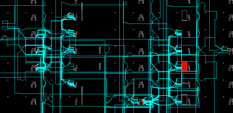
block diagram in RTL-Viewer is as follows: In PlanAhead, the placement of the complex multiplier is shown in the following figure. FPGA Kintex-7, XC7K70TFBG484-1C .

It can be seen that as a result of a complete trace of the project, a processing frequency of the order of ~ 300 MHz is achieved . In practice, this figure is ~ 30% higher.
In the FPGA Editor, the block of a conventional FP23 multiplier looks like this:
As a result of the work, a specialized data format for the FP23 floating point FPGA was developed. It differs from the traditional IEEE 754 format and is sharpened for FPGA processing at maximum speeds. Unlike standard solutions from Xilinx and Altera, nodes in the FP23 format consume significantly less crystal resources. The addition and multiplication operations in FP23 have found application for the implementation of FIR filters and the FFT / IFFT node on the FPGA.
If you wish, you can create your own data format " FP_X " for specific tasks with arbitrary bit depths of the mantissa and exponent. In this case, it is necessary to take into account the features and structure of specific FPGAs.
My articles on similar topics:
Thanks for attention! To be continued...
This article will focus on floating point numbers and, in particular, on the implementation of the specialized FP23 format on programmable logic integrated circuits (FPGAs). As part of a specific project, I had the idea to implement a floating-point data format that is optimal for certain needs. As a result, this idea turned into a real project, which subsequently found application in some interesting tasks of digital signal processing. The article discusses the main difficulties in implementing the floating point data format on the Xilinx FPGA, and considers the basic mathematical operations in the FP23 format. Also at the end of the article you can find the source code of the project, which can be freely used in your tasks or based on it to implement similar data formats.
Data format
Floating-point numbers are actively used in modern signal processors, video cards, and even in FPGAs. In accordance with the IEEE 754 standard , they are represented as a combination of exponent (exponent), mantissa and sign. Numbers in the IEEE 754 standard have 32 bits ( float ). For the sake of clarity, writing numbers in a float is written in normal form or reduced to a normalized form after mathematical operations and transformations on numbers. The range of possible values depends on the number of bits of the mantissa and exponent. Float is characterized by fixed relative accuracy and variable absolute accuracy. Main advantages and disadvantages of numbers in float format:
- + A very wide range of possible values is provided;
- + Achieved high accuracy calculations;
- - Rounding very large numbers to possible values from the grid;
- - Loss of accuracy when summing numbers that differ from each other many times;
- - The complexity of implementation and application on FPGAs.
For modern FPGA chips, the implementation of floating-point numbers is not difficult. For leading manufacturers - Xilinx and Altera, there are ready-made SOFT IP cores that implement float according to the standard. For Altera, the latest families have HARD IP cores that implement the IEEE 754 format on DSP blocks.
Digital part
The main element base for performing mathematical operations and tasks of digital signal processing is advanced FPGA families. The work is carried out on the FPGA company Xilinx, which contain blocks of vectors of configurable cells. First of all, these are universal blocks of digital processing and mathematics - DSP48E1 (for FPGAs of the Virtex-6 series and 7 families) and DSP48E2 (for FPGAs of the UltraScale family). These blocks allow you to perform the functions of addition and subtraction of numbers, shift and transfer, high-speed multiplication, accumulation multiplication (MACC), checksum search, etc. On DSP48 cells in modern FPGAs, many tasks are performed - the development of CIC and FIR filters, high-speed calculation of FFT / IFFT, the implementation of digital frequency synthesizers (DDS and CORDIC), the creation of various formats for presenting data and a set of operations for them.
The second basic component of FPGAs is block memory. For Xilinx FPGAs, these are RAMB36E1 (or RAMB18E1) cells. These are two-port memory elements implemented inside crystals in the form of columns of identical blocks. The number of columns of internal memory depends on the size of the chip. The maximum capacity of a memory block is 36Kbit, while it can be configured as two independent blocks of 18Kbit each. The memory can be used with a data width of 1 to 72 bits. In the absence of free resources of FPGA block memory, you can use distributed memory in special SLICEM cells. For Ultrascale FPGAs, the amount of such memory is up to 512x1, with the possibility of reconfiguring the depth and bit depth of the bus.
Formulation of the problem
Given the above features for the implementation of the analog and digital parts, the task is formed as follows. Let the bit capacity of the data entering the FPGA chip with ADC chips be 16 bits. As the FPGA selected the smallest chip Kintex-7. The task is to translate the 16-bit signed integer FIX16 into a specialized floating-point format FP23 and vice versa, while ensuring maximum processing speed inside the FPGA with minimal expenditure of crystal resources . In addition, it is necessary to designate and implement a set of basic mathematical operations - addition, subtraction and multiplication.
FP format implementation
FP23 is a special format for representing floating point numbers. Unlike the IEEE 754 standard, the word length in FP23 format is not 32 bits, but only 23 bits. The following formula is a simplified representation of the number reflects the «A» in FP format:
Mantissa ( mantissa) in FP23 format is a 17-bit positive number. It is always displayed in a normalized form as a result of all transformations, i.e. the most significant bit of the mantissa is always “1”. To save crystal resources and simplify writing, the 17th bit of the mantissa is never displayed in the packed resulting 23-bit word (see the figure). Therefore, when calculating mathematical operations and translating from one format to another, it is necessary to remember that the mantissa is normalized, and the value 216 must be added to the 16-bit non-zero number. The exponent or exponent in the FP23 format is a 6-bit positive number that determines how much is the mantissa multiplied. Under the sign ( sign) the remaining one bit is highlighted, with a zero value of the bit corresponding to positive numbers, and a single value determining negative numbers. Thus, the number A in FP23 format is described by three bit fields: “exponent” (EXP (A)) , “sign” (SIGN (A)) and “mantissa” (MAN (A)) .
Table 1 shows the bit depth of the data, the range of possible values of the mantissa and exponent, etc.
So, the first step in developing a floating-point data format on an FPGA is to convert a signed fixed-digit integer to the FP23 floating-point format, while ensuring maximum processing speed inside the FPGA. The second step is the inverse conversion of numbers from the FP23 format to a fixed-point format with the ability to scale the output to a specific division factor. And finally, at the third stage, to fully utilize the full power of the FP23 format, it is necessary to implement mathematical operations - addition, subtraction and multiplication.
Before describing the FP23 modules, it is necessary to answer the natural question: “Why is the data capacity in the format exactly 23 bits?” The answer consists of several components. Firstly, one bit is used for the character and the 15 remaining bits for the integer part, so the mantissa and character occupy at least 16 bits. For an exponent, taking into account the offset in the formula, a minimum of 5 bits is required. The more bits are allocated to the exponent, the larger the result (the range of possible values is expanded). Let the exponent have 6 digits, and the mantissa is represented as a 16-bit number, 1 digit is assigned to the sign. Then, to represent numbers in the FP23 format, exactly 23 bits are used. If you use the hidden bit of the mantissa, which is equal to 1 for non-zero values and equal to 0 for zero values of a binary number, then the bit capacity is 24.
In addition, the value "23" was not chosen randomly, because in the future, FPGA memory is required to store the vector of complex values. A pair of values without displaying a hidden bit has a total capacity of 46, with a hidden bit of 48, which fits exactly three RAMB18E1 memory blocks in width. Also, for a pair of values, you can use the additional functions of the DSP48E1 ¬ block — quick comparison of two numbers, parity, and quick summation in SIMD mode.
Convert FIX16-to-FP23
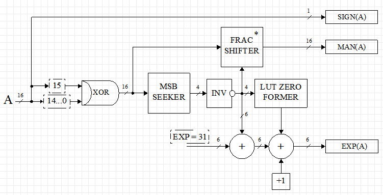
To convert data from the integer character type FIX16 to the FP23 format, it is necessary to use the FPGA chip logic and the built-in DSP48E1 multipliers. The figure shows a block diagram of the conversion of data into the FP23 format.
The maximum bit depths of the DSP48E1 block factors are 25 and 18, respectively, where the most significant bit is significant. To multiply numbers without regard to the sign in the DSP48E1 module, the effective bit depth of the input data is reduced by 1 bit. The converter does not use RAMB18E1 block memory.
Accordingly, in order to find the sign of a number, it is necessary to take the most significant (signed) bit of the input data. The search algorithm for the mantissa MAN (A) based on the FPGA primitives is as follows:
- take the module of the input number (operation "exclusive OR"),
- search for the most significant bit (MSB SEEKER),
- on the most significant bit to form the shift value of the mantissa,
- multiply the modulus of the number and the shift value to obtain the normalized mantissa (FRAC SHIFTER).
To search for the exponent EXP (A) you need:
- take the module of the input number (operation "exclusive OR"),
- search for the most significant bit (MSB SEEKER),
- subtract the inverted index of the significant bit from the number “32”,
- add 1 to the result, taking into account the logic of searching for a non-zero input value (LUT ZERO FORMER).
Since the mantissa is obtained by multiplying the modulus of the real number by some “mask”, on which the shift of the unsigned input number depends, then to find it you need the DSP48E1 block. The procedure for searching and forming the mantissa occurs in the FRAC SHIFTER node and is shown in the figure.
As you can see, the mantissa is formed in two stages. At the first stage, using the LUT logical resources, a 16-MSB factor 2 is created from the input number. In the second stage, the input data is multiplied by the amount of shift in the DSP48E1 node. At the output of the multiplier, a normalized mantissa is formed. According to the description, for multiplying unsigned numbers, the maximum bit depth of one of the factors of the DSP48E1 block is 17, therefore, the mantissa and the generated shift cannot have a large bit depth. This restriction once again leads to the fact that the mantissa of numbers in the FP23 format has a bit capacity of 17. The highest bit of the mantissa for nonzero numbers is 1, it is reserved and is used in the search operation for the resulting mantissa, but is not displayed in the output representation of the number for the normalized form. This bit can be deduced and used in the general representation of the word, then the bit depth of the output word is 24 bits.
To reduce the amount of consumed crystal resources, the DSP48E1 block can be excluded. Then the mantissa search node is converted to a fast shift register (Barrel shifter). For some FPGA crystals, the number of DSP48E1 is small, and the extra waste of resources is critical, so when using FP23 blocks, it is possible to choose one or another option. In addition, for the fast shift option, the total delay for the complete conversion operation is reduced by one clock cycle.
Summing nodes for searching for the exhibitor are made in the form of full binary adders, for the implementation of which the logical components MUXCY, XORCY and CARRY CHAIN are used, which are included in the base cells SLICEL and SLICEM. A detailed description can be found in any literature on programmable logic.
Timing Chart Example
Converting data from FIX to FLOAT FP23:
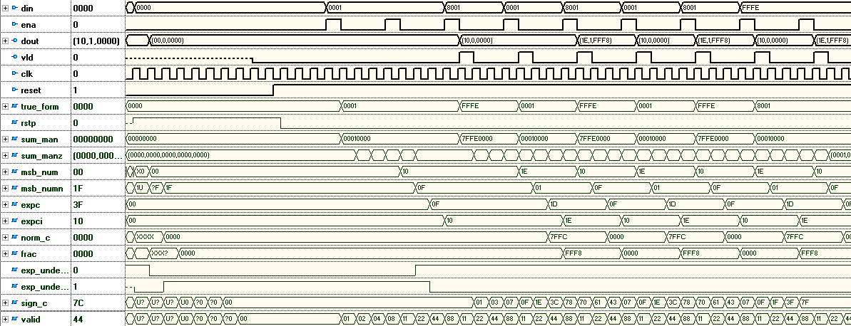
DIN - input data, 16 bits. DOUT - a number in FP23 format, divided into three fields: {EXP, SIGN, MANT} .
DIN - input data, 16 bits. DOUT - a number in FP23 format, divided into three fields: {EXP, SIGN, MANT} .
Convert FP23-to-FIX16
Converting data from the FP23 format to FIX16 takes four steps.
The binary signed number A search algorithm consists of several sequential actions:
- subtract the value SCALE (scaling of the output data) from the exponent EXP (A),
- form a shift mask 2 (EXP (A) -SCALE),
- add the hidden bit IMPL (A) to the mantissa and multiply the result by the amount of shift,
- take into account the sign of the number SIGN (A) by taking the operation “exclusive OR”.
As for the node for direct conversion to FP23 format, in this scheme, to save FPGA resources, the DSP48E1 block can be replaced with a fast shift register executed on SLICEM cells.
Multiplication
Multiplication of numbers in the FP23 format is one of the simplest and most logical operations. The hardware multiplication algorithm is implemented as follows (see. Fig.).
- mantissa multiplication in node DSP48E1,
- normalization of the mantissa (taking bits [32 ... 17] or [31 ... 16] as the mantissa, depending on the value of the most significant bit),
- addition of exhibitors
- subtraction of the number 16 from the sum of the exponentials,
- if the 33rd bit of the mantissa product is “0”, then another 1 is subtracted from the exponent of the result,
- determination of the sign of a work using the “exclusive OR” operation.
The logic of multiplication by a zero number is not reflected in the scheme, but algorithmically it reduces to the fact that if the exponent of any input number is equal to zero, then the output result is also equal to zero. On FPGAs, a zero search is organized using the AND and OR logic functions on the LUT base units.
The number 16 is subtracted from the sum of the exponentials to account for the hidden bits in the mantissa of the input numbers, which give an increase to the exponents. Adders and subtracters in the node for multiplying numbers in a floating point are also implemented according to the binary full adder scheme.
Addition and Subtraction
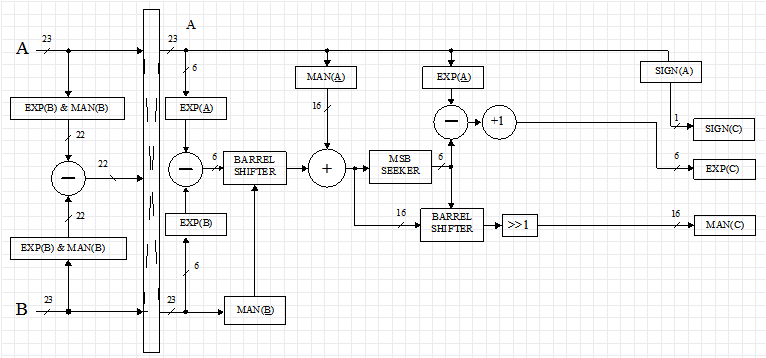
Adding and subtracting numbers in FP23 format is the most resource-consuming operation (see fig.). The addition of numbers in the FP23 format consists of the following fundamental stages:
- reduction of operands to one exponent (alignment),
- Mantissa addition
- normalization of the result (selection of such an exponent so that the 16-bit mantissa is equal to "1").
Hardware addition algorithm is implemented as follows:
- operands "A" and "B" are compared modulo if | A | <| B |, the numbers are interchanged,
- the difference between the exponentials of the operands is calculated, and the result determines how many digits it is necessary to shift the mantissa of the number "B" to the right to bring the numbers to one exponent,
- according to the difference of the exponentials, a number is formed by which the mantissa of the number "B" is multiplied,
- the result of multiplication is added to the mantissa of the number "A",
- in the received number, the number of the most significant bit of the MSB is determined, a number is formed,
- normalization of the mantissa by multiplying the sum of the mantissa by a number,
- exponent of the number EXP © = EXP (A) - MSB + 1.
Subtraction is implemented similarly to addition. The only difference is that the sign SIGN (B) is inverted for the subtracted operand . DSP48E1 units can also be replaced with a fast shift register.
Resources
The synthesis results and the propagation delay for the operation for each node are summarized in table 2. The table shows that the simplest and fastest operation is the multiplication of two numbers in the FP23 format.
The amount of occupied resources after synthesis for all nodes is given in a common log file. Example synthesis results for fp23 multiplier:
Top Level Output File Name         : fp23_mult_m1.ngc
Primitive and Black Box Usage:
------------------------------
# BELS			: 106
#      GND		: 15
#      INV		: 1
#      LUT2		: 25
#      LUT3		: 16
#      LUT4		: 6
#      LUT6		: 14
#      MUXCY		: 14
#      VCC		: 1
#      XORCY		: 14
# FlipFlops/Latches	: 75
# Shift Registers	: 8
#      SRLC16E		: 8
# DSPs			: 1
#      DSP48E1		: 1
Source
All nodes of the FP23 format are written in the VHDL language. For convenience and verification, a small program has been written in C ++ that contains the functions of the implemented operations in a floating point on the FPGA. With its help, you can debug and implement other floating-point formats with other dimensions of the exponent and mantissa.
For the convenience of reading data on VHDL, a type has been created that defines a number in a floating point format. All components and types of FP23 are collected in the file fp_m1_pkg.vhd
type fp23_data is record
	exp 	: std_logic_vector(5 downto 0);
	sig 	: std_logic;
	man 	: std_logic_vector(15 downto 0);
end record;
The source code for the RTL descriptions, the testing program, and the synthesis results can be found on the github link .
Test case
To test all the developed nodes, I came up with a small circuit. This is a complex multiplier, at the input and output of which the data are presented in integer form, and the intermediate results in a floating point. That is, the input is converted to FP23 format. In this format, complex multiplication is implemented, and the result is transferred back from FP23 to a fixed point. The
block diagram in RTL-Viewer is as follows: In PlanAhead, the placement of the complex multiplier is shown in the following figure. FPGA Kintex-7, XC7K70TFBG484-1C .
It can be seen that as a result of a complete trace of the project, a processing frequency of the order of ~ 300 MHz is achieved . In practice, this figure is ~ 30% higher.
In the FPGA Editor, the block of a conventional FP23 multiplier looks like this:
Conclusion
As a result of the work, a specialized data format for the FP23 floating point FPGA was developed. It differs from the traditional IEEE 754 format and is sharpened for FPGA processing at maximum speeds. Unlike standard solutions from Xilinx and Altera, nodes in the FP23 format consume significantly less crystal resources. The addition and multiplication operations in FP23 have found application for the implementation of FIR filters and the FFT / IFFT node on the FPGA.
If you wish, you can create your own data format " FP_X " for specific tasks with arbitrary bit depths of the mantissa and exponent. In this case, it is necessary to take into account the features and structure of specific FPGAs.
My articles on similar topics:
Literature
Thanks for attention! To be continued...