February 6, 2015 at 15:13
Minesweeper on FPGA
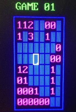 Hello everybody!
 After reading the article “Making Tetris for FPGA” , I remembered that I had a similar project lying around that I had once used for a kind of offer of “hands and hearts” to my girlfriend.
And why not do something similar to yourself?
Digging out the sources, he renewed the lost knowledge and decided on the basis of the old project to whip up a simple version of the game “Minesweeper” on the old FPGA Spartan3E. Actually, the implementation of the Minesweeper game at the level of logic gates and the main features of the development on Xilinx FPGAs will be discussed in this article.
Debug board
A few years ago I was looking for a budget option for a debugging board with FPGAs and the simplest binding to different interfaces such as VGA, PS / 2, the presence of LEDs and an LED display, as well as trigger switches. Then I settled on the simplest Chinese whale, which was easiest to order with ebay for $ 135.00, taking into account delivery. By the way, the kit came incomplete, so I left an angry review, for which the seller returned ~ $ 20. So the board cost me ~ 4000r at the old prices.
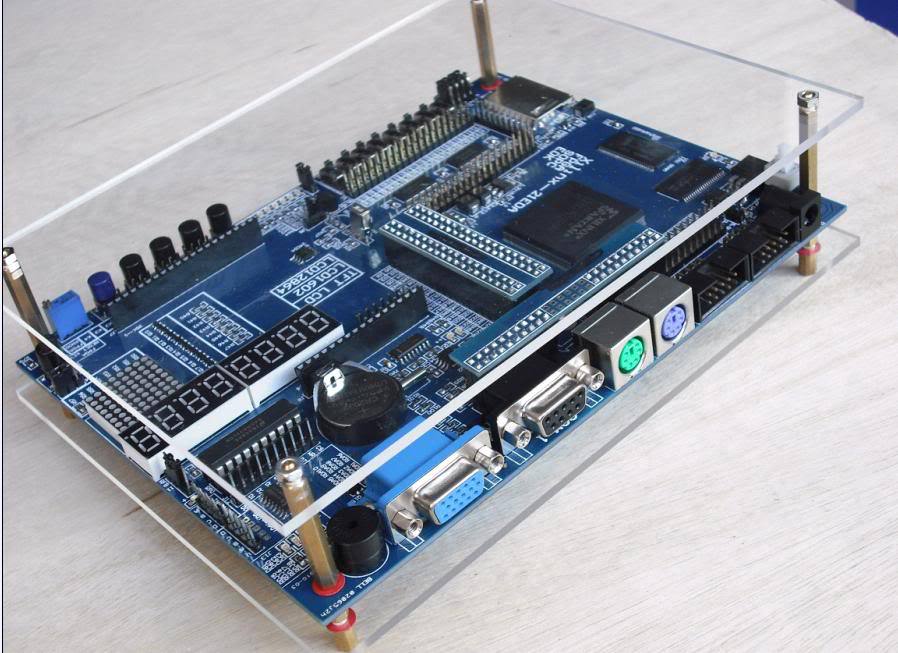
Official website of the whale manufacturer.
The main features of devkita:
- FPGA Spartan3E ( XC3S500E-4PQ208C ) - 500K logic gates,
- Clock source CLK = 50 MHz,
- External memory 64M SDRAM,
- SPI Flash (M25P80) for storing FPGA firmware,
- LED matrix 8x8, LED line 8 pcs.,
- 8 switches and 5 buttons,
- Connectors for LED displays,
- VGA connector for display
- PS / 2 connectors, etc.
The resources of the Spartan3E XC3S500E crystal are shown in the table:
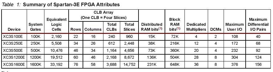
Of all the variety, VGA and PS / 2 connectors are required to implement the Minesweeper game . Apart from them, I used a switch to global reset ( the reset ) logic in the FPGA.
The basic concept of the game
What happened?
The following things were implemented in the old project:
- input of commands from the keyboard (control of the PWM modulator and display);
- Self-written VGA interface with a resolution of 640x480;
- a blinking heart on a matrix of 8x8 LEDs based on PWM.
The first two points significantly accelerated the development time of the game, so I did not invent a bicycle.
Rules for the game:
- Keyboard control:
" WSAD " - arrow buttons to move around the screen;
" Enter " - check the field for the presence / absence of mines;
" Space " - start a new game;
" Esc " - complete the current game;
" Y / N " - to start a new game; - Field 8x8, only 8 min per field;
- The rest of the rules are like in a normal sapper game;
FPGA programming language: VHDL .
This is how the finished project in the PlanAhead program looks after the stages of synthesis and tracing. Blocks in purple frames are the occupied resources of the crystal.
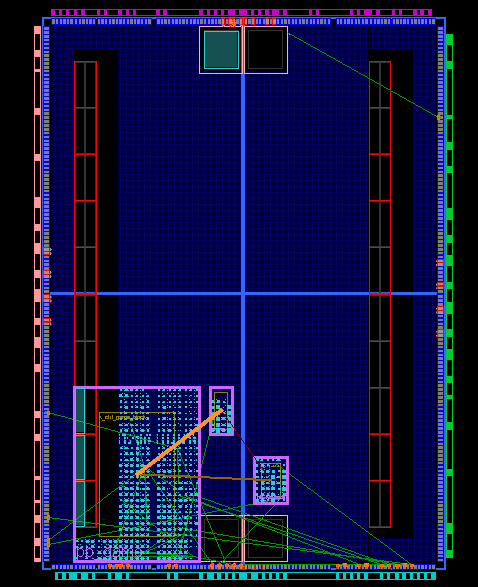
Big block: the main logic of the game;
Middle block: PS / 2 keyboard controller;
Small block: VGA display controller.
Project hierarchy:
At one of the first stages of design, you need to figure out how the project will look and how many components it is more convenient to describe. I came up with the following structure:
-> Top level
----> PS / 2
controller ----> VGA 640x480
controller ----> Game controller
-------> Block for drawing borders of a rectangle,
-------> Block for drawing painted fields 8x8
-------> Block for drawing mines and numbers on the field
-----------> Memory for placing mines
---- -------> Memory for characters
-------> Block for drawing text and dialog messages
-----------> Memory for characters
This is how it looks in the PlanAhead environment from Xilinx.
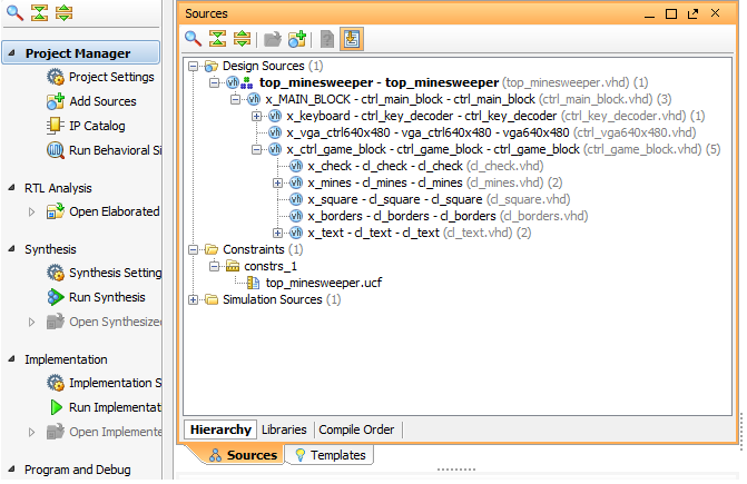
The upper level
It describes the main input-output ports, contains a DCM frequency synthesis unit for converting the input frequency from 50 MHz to 25 MHz. The top-level code is as follows:
entity top_minesweeper is
	port(
		-- PS/2 IO --
		PS2_CLK		:  in  std_logic; -- CLK from PS/2 keyboard
		PS2_DATA	:  in  std_logic; -- DATA from PS/2 keyboard
		-- CLOCK 50 MHz --
		CLK		:  in  std_logic; -- MAIN CLOCK 50 MHz
		-- VGA SYNC --
		VGA_HSYNC	:  out std_logic; -- Horizontal sync
		VGA_VSYNC	:  out std_logic; -- Vertical sync
		VGA_R		:  out std_logic; -- RED
		VGA_G		:  out std_logic; -- GREEN
		VGA_B		:  out std_logic; -- BLUE
		-- SWITCHES --
		RESET		:  in  std_logic -- Asynchronous reset: SW(0)
	);
end top_minesweeper;
PS / 2 controller This project is
taken as a basis . Earned right away. The serial transmission interface is quite primitive: two lines: PS2_CLK and PS2_DATA , along which the keyboard commands go. Pitfall - initially with the help of the “Make” code I generated a single impulse (along the edge) that would signal a “keystroke” of the key. This led to a simulated re-press when another key was pressed. Since the byte “Make” and “Break” codes coincide, we had to make the condition more explicit, given the “Break” code. The code table for the PS / 2 controller is given in the link above. VGA controller
Once, for educational purposes, I wrote on my own, but the algorithm of its operation is exactly the same as with all VGA controllers . On Habré too is such .
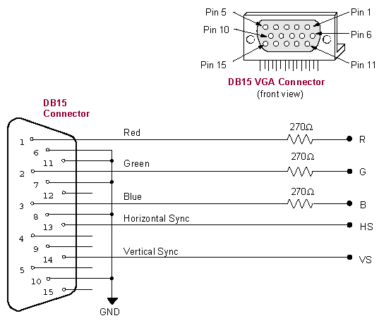
Key features:
- Controller frequency: 25.175 MHz
- Screen resolution: 640x480
- Update frequency: 60Hz
- Available palette: RGB
Unfortunately, the debug board does not have built-in decryption chips for the color palette, so only 3 primary colors are available (red, green, blue ) and 5 combinations (yellow, magenta, cyan, white and black). But this does not stop to come up with a color scheme and even display blinking images! (see video at the end)
Game controller
The easiest way to describe the Sapper game controller is based on a state machine ( FSM ). It is necessary to come up with the conditions of the machine in which certain events will be processed.
My project uses 5 basic combinations of the machine:
- WAIT_START (resetting all control signals, min counter, starting random game generator;
- PLAY (game process: control buttons from the keyboard, mine search);
- CHECK (check if a mine is found - go to the end of the game);
- GAME_OVER (determines the event of victory or defeat, displays additional messages on the display);
- RST (optional stage - clears the screen, resets all control signals, without the possibility of starting a new game).
Symbol memory
Found on the Internet . The dimensions of one character are 8x16. Example for symbol "1":
	"00000000", -- 0
	"00000000", -- 1
	"00011000", -- 2
	"00111000", -- 3
	"01111000", -- 4    **
	"00011000", -- 5   ***
	"00011000", -- 6  ****
	"00011000", -- 7    **
	"00011000", -- 8    **
	"00011000", -- 9    **
	"00011000", -- a    **
	"01111110", -- b    **
	"00000000", -- c    **
	"00000000", -- d  ******
	"00000000", -- e
	"00000000", -- f
All characters fit into a single block of RAMB16 crystal block memory. The memory is arranged in such a way that the symbol consists of 16 vectors with a capacity of 8. To display the symbols, the lower 4 bits of the address bus must be connected to the Y coordinate vector. Logical '1' - colors the symbol in color, '0' - background color (black).
Memory for placing mines on the field
I modified this part of the project the longest, inventing various sophisticated solutions. In the end, I decided to make the next component in the form of ROM-memory, which selects the game.
Piece of code:
constant N8x8	: integer:=8; -- константа поля 8х8
constant Ngames	: integer:=1; -- количество игр
type round_array_3x64xN is array (Ngames*N8x8*N8x8-1 downto 0) of integer range 0 to 7;
constant mem_init0:	round_array_3x64xN:=(
	-- game 0:
	1,1,1,0,0,0,0,0,
	1,7,1,1,1,1,0,0,
	1,1,1,1,7,2,1,0,
	0,0,0,1,2,7,1,0,
	0,1,1,1,1,1,1,0,
	0,1,7,2,7,1,1,1,
	0,1,1,2,2,2,2,7,
	0,0,0,0,1,7,2,1);
The constants N8x8 and Ngames specify the size of the field and the number of games. The number on the field corresponds to the mine or the number of mines around it. The rules are very simple:
- Numbers 0-6 - determine the number of mines,
- Number 7 - reserved and defines a mine on the field.
Why is that?
I did not come up with a situation where 7 or 8 minutes could be immediately around a point. For 8 minutes and an 8x8 field, these are too uninteresting decisions. In addition, numbers from 0 to 7 occupy only 3 bits, while combinations from 0 to 8, and 9 for a mine already occupy 4 bits. In this regard, I am a big fan of saving the internal logic and trace resources of the crystal, even if these resources are enough for 5 projects.
Thus, all numbers fit into a kind of ROM-array, which can be added with your games. My project has 32 games, which takes a little less than 1 RAMB16 memory block. It should be noted that numbers are specified in integer format . To translate them into std_logic_vector (2: 0)and further processing a special function is written. The integer format simplified the recording of new games and significantly saved time. Many VHDL FPGA developers are sometimes led into a stupor by the situation when an integer format is used, since constructions with an integer type are not always synthesized, i.e. they can not be checked in real hardware. But for a ROM generator, integer is the best choice.
In order to add your own layout of mines - you need to correctly fill out the 8x8 field in the array. Variations of games stuffed by hand. In total in my project 32 different combinations of placement of mines.
Blocks for drawing borders and fields 8x8
Initially, I implemented them on a symbol generator, but then I decided to save crystal resources, because I thought that for the sake of the shaded squares and the frame, it makes no sense to use the whole RAMB16 cell. (Optimization by resources!) Therefore, everything is done on multiplexers. I will not dwell on this in detail.
Block for drawing mines and numbers
Converts data from the memory of the set of games into numbers and mines on the screen, using the memory of characters. Initially, I wanted to bring out a 8x8 square field, but then I became too lazy to rewrite the ROM generator, and I left it rectangular.
For this block, I also had to create a special 8x8 mask, with which, by pressing “Enter”, the filled cells would turn into a digit or a mine.
Text and Messages
The text is written in one piece - that is, everything is written on the screen at once, but depending on the stage of the game, some information remains invisible (for example, messages about defeat or victory). The same character generator is used. The size of the symbol is 8x16, so the display field of 640x480 can be divided into sections 80x30, in which the symbols are displayed. How it's done?
Below is a simple example:
addr_rom <= data_box(6 downto 0) & y_char(3 downto 0) when rising_edge(clk);
x_char_rom: ctrl_8x16_rom -- память коэффициентов
	port map (
		clk	=> clk,
		addr	=> addr_rom,
		data	=> data_rom);
pr_sel: process(clk, reset) is -- данные для отображения на дисплей
begin
	if reset = '0' then
		data <= '0';
	elsif rising_edge(clk) then
		data <= data_rom(to_integer(unsigned(not x_char(2 downto 0))));
	end if;
end process;
g_rgb: for ii in 0 to 2 generate -- окрашивание данных в цвет
begin
	rgb(ii) <= data and color(ii);
end generate;
First you need to figure out how to use a memory address to select one or another character. It can be seen that the address consists of two vectors “y_char” and “data_box”.
y_char (3 downto 0) are the least significant bits of the coordinate vector along the Y axis. This data is updated automatically and comes from the VGA controller.
data_box (6 downto 0) - the signal selects which character will be used on the field. This vector must be written yourself.
If we write data_box <= "000001", then the first character from the generator is written to the vector "data_rom". In the pr_sel process, the data vector is converted to serial code. Depending on the 3 least significant bits of the X coordinate register, a specific bit of the data_rom vector is selected. At first, I ran into the problem of mirroring data on the screen. The solution is trivial - inversion of the x_char signal.
The output is an RGB signal that is fed to the VGA connector after a logical conversion with data from the coefficient memory.
Realization in iron
All this is going to one big project. For beauty, with the help of a simple counter, I screwed up the blinking of victory / defeat messages, and also added a generator to select a random game.
The * .UCF file, which describes the connection of FPGA ports and various attributes, is surely screwed to the sources on VHDL. Example:
## Switches
NET "RESET"	LOC = "P148" | IOSTANDARD = LVTTL | PULLUP ; ## SW<0>
NET "ENABLE"	LOC = "P142" | IOSTANDARD = LVTTL | PULLUP ; ## SW<1>
## VGA ports
NET "VGA_R" 	LOC = "P96" | IOSTANDARD = LVTTL | DRIVE = 8 | SLEW = FAST ;
NET "VGA_G" 	LOC = "P97" | IOSTANDARD = LVTTL | DRIVE = 8 | SLEW = FAST ;
NET "VGA_B" 	LOC = "P93" | IOSTANDARD = LVTTL | DRIVE = 8 | SLEW = FAST ;
NET "VGA_HSYNC" LOC = "P90" | IOSTANDARD = LVTTL | DRIVE = 8 | SLEW = FAST ;
NET "VGA_VSYNC" LOC = "P94" | IOSTANDARD = LVTTL | DRIVE = 8 | SLEW = FAST ;
## CLK 50 MHz
NET "CLK" 	LOC = "P183" | IOSTANDARD = LVCMOS33 ;
NET "CLK" TNM = "CLK_TN";
TIMESPEC TS_CLK = PERIOD "CLK_TN" 20 ns HIGH 50%;
# PS/2 KEYBOARD
NET "PS2_CLK" 	LOC = "P99" | IOSTANDARD = LVTTL | DRIVE = 8 | SLEW = FAST ;
NET "PS2_DATA" 	LOC = "P100" | IOSTANDARD = LVTTL | DRIVE = 8 | SLEW = FAST ;
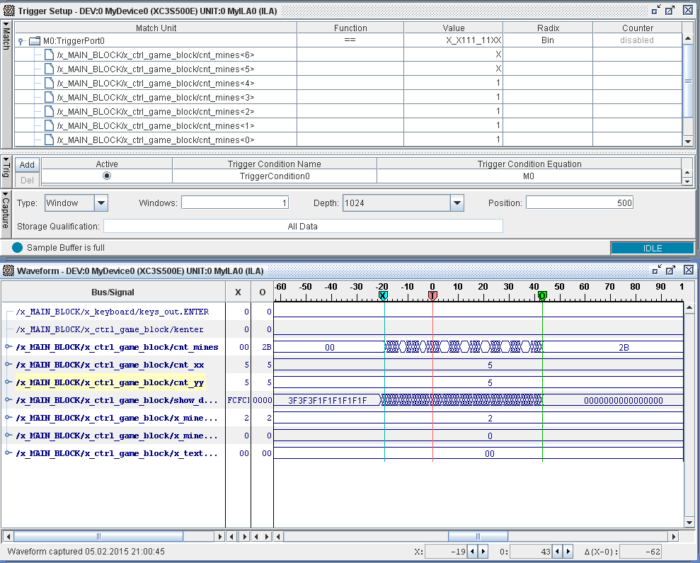
Using Aldec Active-HDL CAD and Xilinx ISE CAD, FPGA design is synthesized and traced. Due to the complexity of event processing, debugging was performed without writing Testbench, directly uploading firmware to the FPGA and checking the output on the display. As a rule, everything worked at once. The main errors were the synchronization of signals. For example, the simultaneous operation of snapping an address and trying to read data. Such errors are corrected quickly by introducing an additional delay per beat in the right place. In severe cases, ChipScope Pro ( Core Inserter and Analyzer ) was used.
Conclusion
The Minesweeper mini-game has successfully earned on the debug board.
The size of the field is 8x8, the number of mines on the field is 8. The
number of games is 32. Before starting, the placement of mines is randomly selected from the memory for the field.
The occupied resources of the crystal (FPGA is almost empty):

Photo
The result looks something like this:
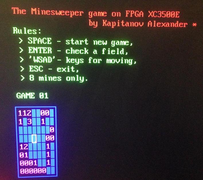
One more photo...
Tracing in FPGA-Editor in the area of the game controller:
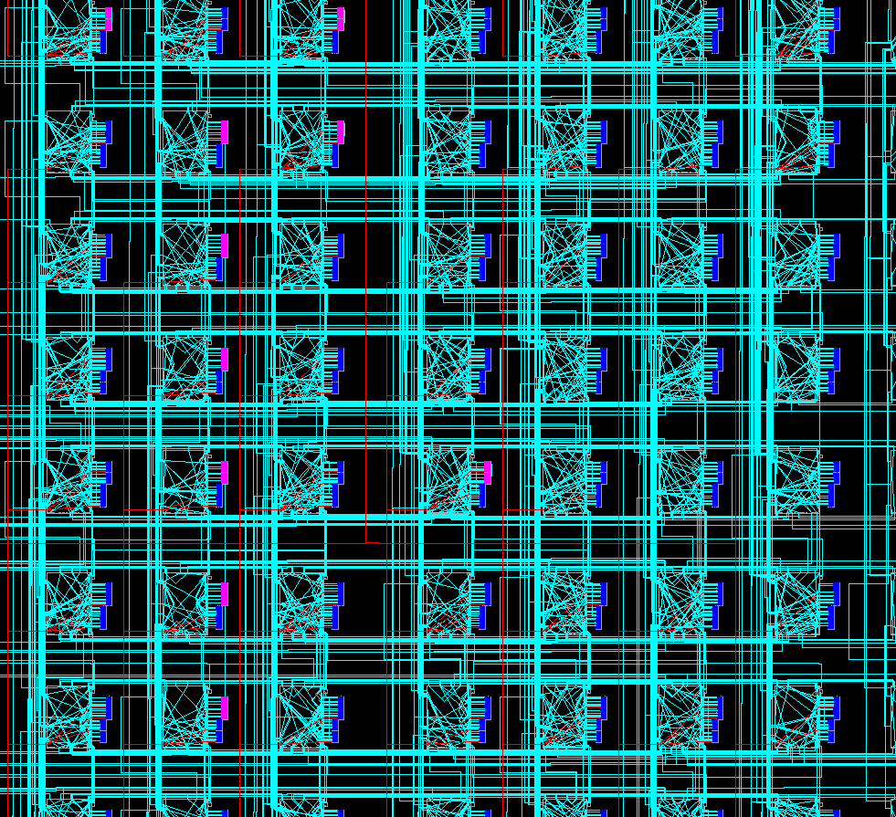
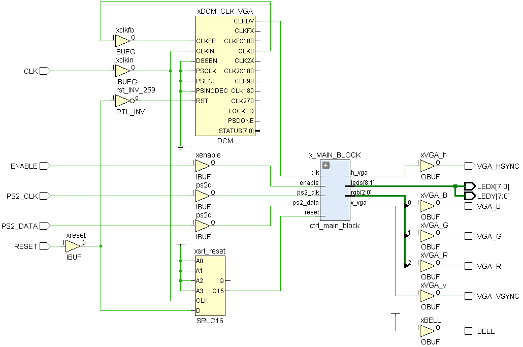
Schematic view of a project in RTL Schematic:
Debugging a project in ChipScope Pro Analyzer (counting the number of open empty fields):
Schematic view of a project in RTL Schematic:
Debugging a project in ChipScope Pro Analyzer (counting the number of open empty fields):
Github source code .
Game Demo