STM32H7 - clocking setting without HAL
Not so long ago, STM launched a very powerful, by the standards of microcontrollers, line of STM32H7 crystals. What attracted me to her:
I thought very well, I soldered the STM32H743IIT6 crystal instead of STM32F746IGT6 and started a new project in SW4STM32.
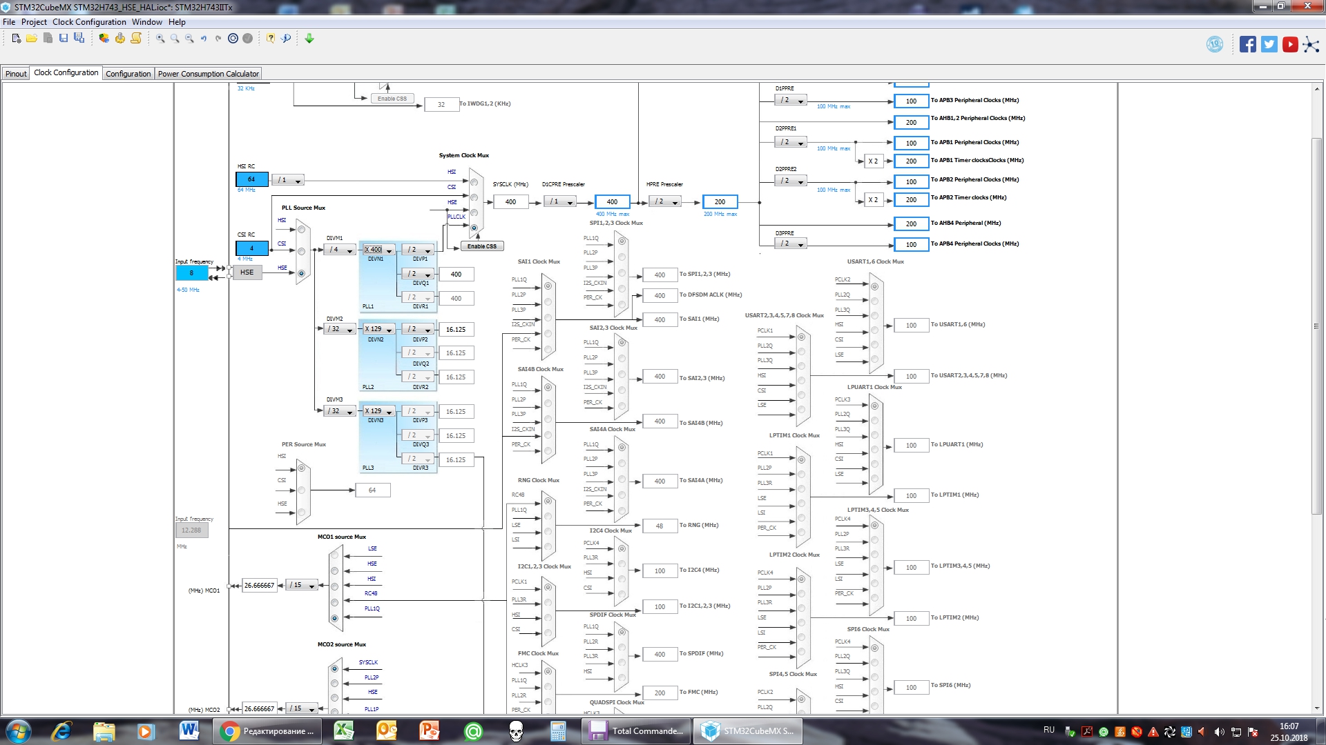
To calculate the coefficients of the dividers and multipliers of the microcontroller clocking system, it is convenient to use the Clock Configuration tab of the STM32CubeMX program.
Clocking settings:
Accordingly, the core frequency (SYSCLK) is 400 MHz.
In addition to the STM32CubeMX, there is also a set of the "STM32CubeH7 firmware package", which contains a large number of examples for working with peripherals for the STM32H7. It was from him was taken the sequence of initialization of the clocking system of the microcontroller.
Information and comments are taken from the following sources:
So, let's begin.
1. Turning on external quartz and waiting for readiness.
2. Specify the frequency source for PLL1 - external quartz.
3. The value of the divider is set to 4.
4. The multiplier N and dividers P, Q, R
5. Fractional PLL frequency divider (if needed)
6. Specify the input frequency range PLL1
7. Specify the output frequency range of PLL1
8. Enable output dividers PLL1: P, Q, R
9. The inclusion of a fractional divider.
10. Start PLL1 and wait for readiness
PLL1 is configured and running. Now select the source of the SYSCLK frequency and set up the bus dividers.
11. Divider by 2 HPRE
12. Without division D1CPRE
13. Set PLL1 as source of SYSCLK and expect readiness.
14. Divider by 2 D1PPRE
15. Divider by 2 D2PPRE1
16. Divider by 2 D2PPRE2
17. Divider by 2 D3PPRE
In order to make sure that the configuration and startup were successfully using the output of the microcontroller MCO2. This output should have a frequency of 26.666 MHz with an output divider of 15.
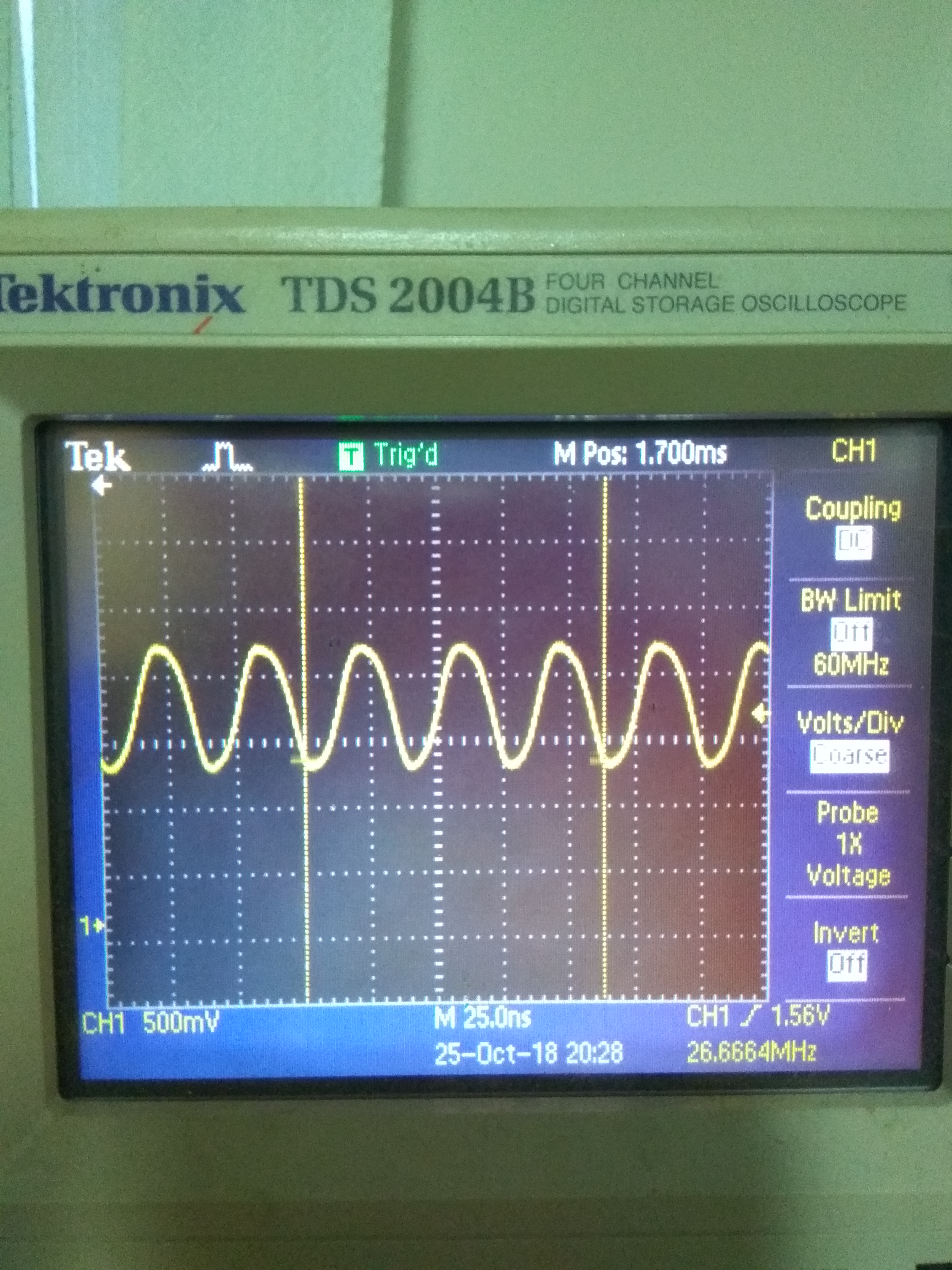
Excellent. The frequency is present, then everything is done correctly.
- increased core frequency up to 400 MHz
- increased RAM, up to 1 MB
- 16 bit ADC
- pin-to-pin compatibility with the F7 series
I thought very well, I soldered the STM32H743IIT6 crystal instead of STM32F746IGT6 and started a new project in SW4STM32.
To calculate the coefficients of the dividers and multipliers of the microcontroller clocking system, it is convenient to use the Clock Configuration tab of the STM32CubeMX program.
Clocking settings:
- outer quartz - 8 MHz
- frequency source for PLL1 - external quartz (HSE)
- divider for PLL1 - 4 (DIVM1)
- multiplier PLL1 - 400 (DIVN1)
- output dividers - 2 (DIVP1, DIVQ1, DIVR1)
Accordingly, the core frequency (SYSCLK) is 400 MHz.
In addition to the STM32CubeMX, there is also a set of the "STM32CubeH7 firmware package", which contains a large number of examples for working with peripherals for the STM32H7. It was from him was taken the sequence of initialization of the clocking system of the microcontroller.
Information and comments are taken from the following sources:
- SystemClock_Config from STM32CubeH7 firmware package
- Reference manual STM32H743 / 753 and STM32H750 advanced ARM-based 32-bit MCUs
- - Datasheet STM32H743xI
So, let's begin.
1. Turning on external quartz and waiting for readiness.
// Enable HSE
	RCC->CR |= RCC_CR_HSEON;
	// Wait till HSE is readywhile((RCC->CR & RCC_CR_HSERDY) == 0);
2. Specify the frequency source for PLL1 - external quartz.
//RCC_OscInitStruct.PLL.PLLSource = RCC_PLLSOURCE_HSE;
	RCC -> PLLCKSELR |= RCC_PLLCKSELR_PLLSRC_HSE;
3. The value of the divider is set to 4.
//PLLM = 4
	RCC -> PLLCKSELR &= ~RCC_PLLCKSELR_DIVM1_5; //0
	RCC -> PLLCKSELR &= ~RCC_PLLCKSELR_DIVM1_4; //0
	RCC -> PLLCKSELR &= ~RCC_PLLCKSELR_DIVM1_3; //0
	RCC -> PLLCKSELR |=  RCC_PLLCKSELR_DIVM1_2; //1
	RCC -> PLLCKSELR &= ~RCC_PLLCKSELR_DIVM1_1; //0
	RCC -> PLLCKSELR &= ~RCC_PLLCKSELR_DIVM1_0; //0
4. The multiplier N and dividers P, Q, R
//PLL1DIVR     bits//DIVN1[8:0]  0  - 8   PLLN = 400//DIVP1[6:0]  9  - 15  PLLP = 2//DIVQ1[6:0]  16 - 22  PLLQ = 2//DIVR1[6:0]  24 - 30  PLLR = 2
	RCC -> PLL1DIVR  |= 0x0101038F;
5. Fractional PLL frequency divider (if needed)
// /* Configure PLL  PLL1FRACN *///__HAL_RCC_PLLFRACN_CONFIG(RCC_OscInitStruct->PLL.PLLFRACN);
	RCC -> PLL1FRACR = 0;
6. Specify the input frequency range PLL1
/* Select PLL1 input reference frequency range: VCI *///__HAL_RCC_PLL_VCIRANGE(RCC_OscInitStruct->PLL.PLLRGE) ;
	RCC->PLLCFGR |= RCC_PLLCFGR_PLL1RGE_3;
7. Specify the output frequency range of PLL1
/* Select PLL1 output frequency range : VCO *///__HAL_RCC_PLL_VCORANGE(RCC_OscInitStruct->PLL.PLLVCOSEL) ;
	RCC->PLLCFGR &= ~RCC_PLLCFGR_PLL1VCOSEL;
8. Enable output dividers PLL1: P, Q, R
/* Enable PLL System Clock output. */// __HAL_RCC_PLLCLKOUT_ENABLE(RCC_PLL1_DIVP);//Bit 16 DIVP1EN: PLL1 DIVP divider output enable
	RCC->PLLCFGR |= RCC_PLLCFGR_DIVP1EN;
    /* Enable PLL1Q Clock output. *///__HAL_RCC_PLLCLKOUT_ENABLE(RCC_PLL1_DIVQ);
	RCC->PLLCFGR |= RCC_PLLCFGR_DIVQ1EN;
    /* Enable PLL1R  Clock output. */// __HAL_RCC_PLLCLKOUT_ENABLE(RCC_PLL1_DIVR);
	RCC->PLLCFGR |= RCC_PLLCFGR_DIVR1EN;
9. The inclusion of a fractional divider.
/* Enable PLL1FRACN . *///__HAL_RCC_PLLFRACN_ENABLE();
	RCC->PLLCFGR |= RCC_PLLCFGR_PLL1FRACEN;
10. Start PLL1 and wait for readiness
/* Enable the main PLL. *///__HAL_RCC_PLL_ENABLE();
    RCC->CR |= RCC_CR_PLLON;
    while((RCC->CR & RCC_CR_PLL1RDY) == 0);
PLL1 is configured and running. Now select the source of the SYSCLK frequency and set up the bus dividers.
11. Divider by 2 HPRE
//RCC_ClkInitStruct.AHBCLKDivider = RCC_HCLK_DIV2;// MODIFY_REG(RCC->D1CFGR, RCC_D1CFGR_HPRE, RCC_ClkInitStruct->AHBCLKDivider);//HPRE[3:0]: D1 domain AHB prescaler//1000: rcc_hclk3 = sys_d1cpre_ck / 2
    RCC -> D1CFGR |=  RCC_D1CFGR_HPRE_3; //1
    RCC -> D1CFGR &= ~RCC_D1CFGR_HPRE_2; //0
    RCC -> D1CFGR &= ~RCC_D1CFGR_HPRE_1; //0
    RCC -> D1CFGR &= ~RCC_D1CFGR_HPRE_0; //0
12. Without division D1CPRE
//RCC_ClkInitStruct.SYSCLKDivider = RCC_SYSCLK_DIV1;//MODIFY_REG(RCC->D1CFGR, RCC_D1CFGR_D1CPRE, RCC_ClkInitStruct->SYSCLKDivider);//D1CPRE[3:0]: D1 domain Core prescaler//0xxx: sys_ck not divided (default after reset)
    RCC -> D1CFGR &= ~RCC_D1CFGR_D1CPRE_3; //0
    RCC -> D1CFGR &= ~RCC_D1CFGR_D1CPRE_2; //0
    RCC -> D1CFGR &= ~RCC_D1CFGR_D1CPRE_1; //0
    RCC -> D1CFGR &= ~RCC_D1CFGR_D1CPRE_0; //0
13. Set PLL1 as source of SYSCLK and expect readiness.
//RCC_ClkInitStruct.SYSCLKSource = RCC_SYSCLKSOURCE_PLLCLK;//MODIFY_REG(RCC->CFGR, RCC_CFGR_SW, RCC_ClkInitStruct->SYSCLKSource);//SW[2:0]: System clock switch//011: PLL1 selected as system clock (pll1_p_ck)
    RCC->CFGR &= ~RCC_CFGR_SW_2; //0
    RCC->CFGR |=  RCC_CFGR_SW_1; //1
    RCC->CFGR |=  RCC_CFGR_SW_0; //1while((RCC->CFGR & RCC_CFGR_SWS) != RCC_CFGR_SWS_PLL1);
14. Divider by 2 D1PPRE
//D1PCLK1 Configuration//RCC_ClkInitStruct.APB3CLKDivider = RCC_APB3_DIV2;//MODIFY_REG(RCC->D1CFGR, RCC_D1CFGR_D1PPRE, RCC_ClkInitStruct->APB3CLKDivider);//Bits 6:4 D1PPRE[2:0]: D1 domain APB3 prescaler//100: rcc_pclk3 = rcc_hclk3 / 2
    RCC -> D1CFGR |=  RCC_D1CFGR_D1PPRE_2;
    RCC -> D1CFGR &= ~RCC_D1CFGR_D1PPRE_1;
    RCC -> D1CFGR &= ~RCC_D1CFGR_D1PPRE_0;
15. Divider by 2 D2PPRE1
//PCLK1 Configuration//RCC_ClkInitStruct.APB1CLKDivider = RCC_APB1_DIV2;//MODIFY_REG(RCC->D2CFGR, RCC_D2CFGR_D2PPRE1, (RCC_ClkInitStruct->APB1CLKDivider));//Bits 6:4 D2PPRE1[2:0]: D2 domain APB1 prescaler//100: rcc_pclk1 = rcc_hclk1 / 2
    RCC -> D2CFGR |=  RCC_D2CFGR_D2PPRE1_2;
    RCC -> D2CFGR &= ~RCC_D2CFGR_D2PPRE1_1;
    RCC -> D2CFGR &= ~RCC_D2CFGR_D2PPRE1_0;
16. Divider by 2 D2PPRE2
//PCLK2 Configuration//RCC_ClkInitStruct.APB2CLKDivider = RCC_APB2_DIV2;//MODIFY_REG(RCC->D2CFGR, RCC_D2CFGR_D2PPRE2, (RCC_ClkInitStruct->APB2CLKDivider));//Bits 10:8 D2PPRE2[2:0]: D2 domain APB2 prescaler//100: rcc_pclk2 = rcc_hclk1 / 2
    RCC -> D2CFGR |=  RCC_D2CFGR_D2PPRE2_2;
    RCC -> D2CFGR &= ~RCC_D2CFGR_D2PPRE2_1;
    RCC -> D2CFGR &= ~RCC_D2CFGR_D2PPRE2_0;
17. Divider by 2 D3PPRE
//D3PCLK1 Configuration//RCC_ClkInitStruct.APB4CLKDivider = RCC_APB4_DIV2;//MODIFY_REG(RCC->D3CFGR, RCC_D3CFGR_D3PPRE, (RCC_ClkInitStruct->APB4CLKDivider) );//Bits 6:4 D3PPRE[2:0]: D3 domain APB4 prescaler//100: rcc_pclk4 = rcc_hclk4 / 2
    RCC -> D3CFGR |=  RCC_D3CFGR_D3PPRE_2;
    RCC -> D3CFGR &= ~RCC_D3CFGR_D3PPRE_1;
    RCC -> D3CFGR &= ~RCC_D3CFGR_D3PPRE_0;
In order to make sure that the configuration and startup were successfully using the output of the microcontroller MCO2. This output should have a frequency of 26.666 MHz with an output divider of 15.
Excellent. The frequency is present, then everything is done correctly.