Do-it-yourself IBM PC is easy
After I realized my long-standing dream and nevertheless (although almost 30 years late) built Radio 86RK , for some time it seemed to me that a quite worthy point was put on this part of my story.
Nevertheless, it was discovered that the disease was not completely cured, and she returned with an even more acute relapse. Probably, the unexpectedly successful experience of building the 86RK affected it, as well as the fact that during this process I formed a rather large number of very attractive looking tools, instruments and parts that I really wanted to find application.
In the end, the withdrawal became unbearable, and I had to take up the soldering iron again and also recall some other skills from the past. What came of this can be seen along with a certain number of pictures and a very (I repeat - VERY) large number of letters (and not even letters, but pages) further ...
The main question was what exactly to do. On the one hand, the soul lay for something quite rare, on the other hand, I also wanted to try new technologies. Being in heavy thought, I periodically looked through a couple of thematic forums devoted to the old hardware. At some point, I came across a long-reaching topic about how to start the 8086 processor with a minimum of binding. It was strange that the topic was discussed for more than a year, but it did not move to the practical plane.
In my inexperienced view, it seemed that the task was generally trivial, but what if there is something there that I don’t understand at all? As a result, I decided to try to play around with this in the hope that this entertainment is exactly what I need for complete happiness.
I didn’t even draw a diagram for myself - everything seems so simple that there were no questions about where to connect what. It only remained to decide how to collect it all. With MGTF I played enough before, I wanted something new. Since everything new is the forgotten old, I bought a tool and materials for wrap-up and started the process. Which (process), unfortunately, didn’t really go anywhere ... Either my hands were growing out of the wrong place, or I understood something wrong, but I couldn’t achieve a stable twist.
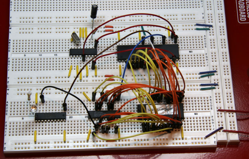
However, I didn’t suffer for long (although maybe this was the main reason?) - in the process of shifting my treasures from place to place, an unopened solderless breadboard with a bunch of very beautiful multi-colored wires was discovered. The complexity (or rather, the lack thereof) of the project made it possible to easily place everything on this board, which I did quite quickly:
A super program of a size of ten bytes was written that implements a function that has no world analogues - blinking an LED. The first time it turned on, nothing worked, but it turned out that the problem was only in starting the clock generator. I was too lazy to put the capacitors / resistors indicated in the documentation near the quartz, so sometimes to start the generator it was necessary to touch the quartz case with a finger or a screwdriver, after which the LED began to flash normally.
By the way, I was a little surprised by the blinking frequency - I already forgot how slow this processor was. At the maximum permissible clock frequency of 5 MHz for the original 8088, a cycle of 65536 "empty" operations was carried out on the order of a second ...
Having published the result of my work on the corresponding forum, I was immediately accused of the fact that the connection to 8086 was discussed, and I have 8088, which is much simpler and in general!
Well, practice is the criterion of truth. I got 8086, spent a little more time (mainly to manually distribute the program in two ROM chips, since 8086 was 16-bit, and I had 8-bit ROMs) and received another flashing light:
Appetite is known to come with eating. So I, instead of satisfaction from what was achieved, had a desire to move on. Only here the idea was firmly established that it was also necessary to try out modern technologies. As an example of modern technology, it was decided to use FPGA in combination with an 8088 processor. In one fell swoop, it was possible to kill several birds with one stone - the base (processor) is familiar, FPGA technologies are quite modern, you don’t need to spend much time on installation, since all the creativity can be transferred inside FPGA.
I already had one of the most sophisticated debugging FPGA boards - Terasic DE2-115, on which, in addition to the rather large FPGA Altera Cyclone IV, an unlimited number of bells and whistles and flashing lights were also installed:
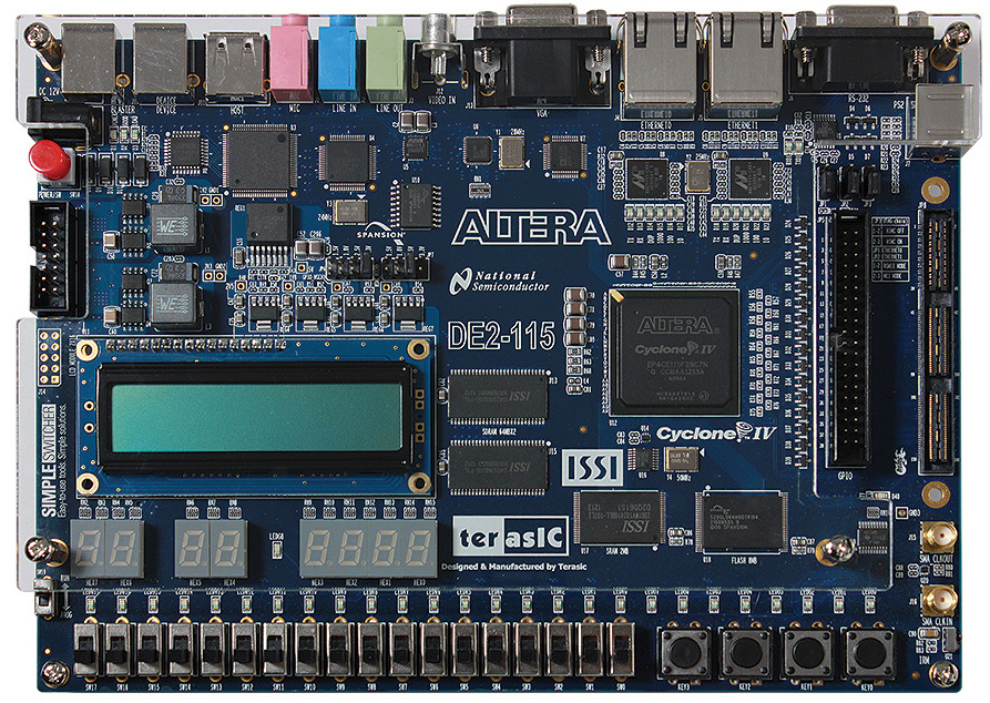
In particular, in addition to the standard 36 GPIOs plus a few more, this board also has an expansion slot, to which you can connect a small board and get a total of about 100 GPIOs, which should be enough for almost any conceivable application (of course, in my modest purposes).
True, there is a nuance - the 8088 processor is 5-volt, but FPGA has long abandoned support for TTL 5V, the maximum that is - LVTTL 3.3V
It is good that there is a wide selection of level converters, which was decided to be used. At first I settled on the TXB0108 chip - an 8-bit bi-directional level converter with automatic direction selection. The automatic choice of direction was quite important, as it allowed us not to think about what was happening on the data bus — reading or writing. In addition, the data bus in 8088 is multiplexed with the 8 least significant bits of the address bus, which adds complexity to determining in which direction the signals should be transmitted - from the processor or to it.
Since the TXB0108 is quite small, and I no longer really wanted to mess with the wires, I decided to try another thing new to me. The Eagle program for PCB layout was purchased, and my torment began both with the development of a new software product in general, and with the very specific Eagle interface in particular.
For me personally, doing something for the first time in a new field is very painful for me - you poke like a blind kitten, and your soul breaks into the open. The preparation of gerber-files for the production of the board (yes, I thought about LUT, and even bought the material, but did not dare) almost caused a nervous breakdown - I immediately imagined how the whole production was standing and laughing, looking at the miserable results of my work ...
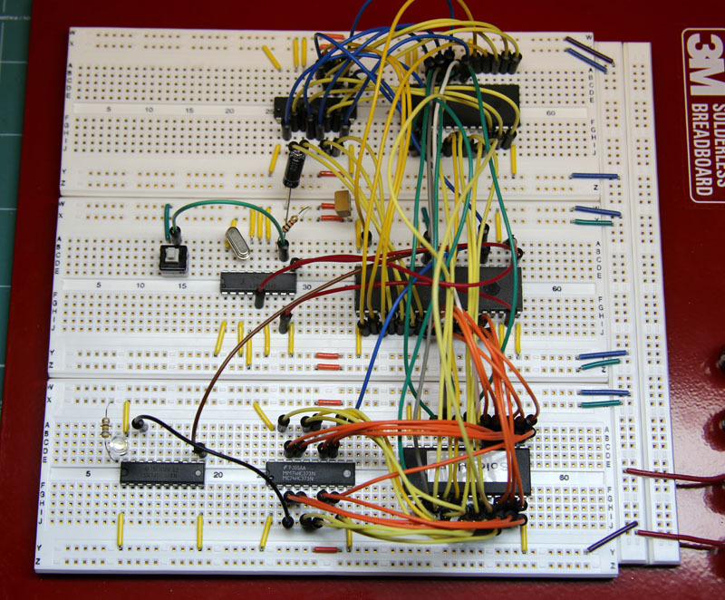
It’s good that the board was very simple, so not even a week passed (along with the manufacturing time), as I already held in my hands a freshly soldered creation:
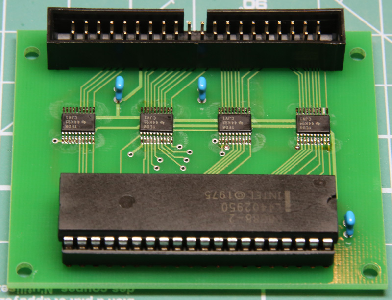
By the way, for soldering level converters I tried the Ersa microwave tip (naturally, there’s a similar from other manufacturers, and you can do this yourself). I must say that it works pretty well, so the complexity of soldering was an order of magnitude less than what might be expected with such sizes of conclusions.
During the time that the board was manufactured, I mastered the FPGA at an accelerated pace. In general, I originally bought a debugging board in order to have some fun with FPGA technologies and, in particular, with VHDL, but this didn’t work for me specifically. The brain simply refused to think in terms of VHDL, and the maximum that I did was repeat several simple devices in FPGA, copying their circuits using the circuit design method. The study of VHDL ended at the level of signal3 <= signal1 and signal2; further reading of the textbooks had an excellent soporific effect on me.
Here, too, I decided to do everything with the help of circuit design. And anyway - what for all these HDLs, when is it so simple to draw a diagram with the mouse and everything works? At that moment it seemed to me both more correct and more convenient. Accordingly, I drew the same flashing light in Quartus, only I had to make an analog of the 8284 clock (I had it in the “iron” form on the breadboard). Fortunately, the documentation found a complete internal structure of this microcircuit, so there were no problems with this. Although one nuance was revealed - in the documentation from Intersil (manufacturer of obsolete chips), the internal structure of 8284 was drawn with an error (inverse output instead of direct, or vice versa - I don’t remember anymore). True, I caught a mistake while considering the scheme, but the fact itself once again led to the idea that we should be guided by the original documents.
Next, a ROM with the corresponding program was generated, my motherboard with a processor connected by a flat cable to the debug motherboard, and the moment of truth came - loading the firmware into the FPGA. Unfortunately, the LED did not blink after that ... After a short trial, it turned out that I applied 0 to one of the processor inputs, whereas there should be 1. This misunderstanding was easily corrected by cutting the track and soldering the jumper. After that, the LED blinked, but froze in a burning state ...
And here the real showdown went. Unfortunately, I will say right away that I did not understand the reason for the unstable operation of the circuit. I’m almost sure that this is due to a fuzzy determination of the direction of signals through level converters (if only because there is nothing more to work wrong with there). The LED could blink for a while, and then generally in complete failure, then again start working without any regularity.
All my poking with the oscilloscope did not show anything that could lead to a true reason, so I had to think about ways to radically solve the problem - pride did not allow me to stop at this place. Since the "self-determining" converters turned out to be a big question, I decided to turn to a more proven solution - 74LVC8T245, level converters with "manual" control of the signal transmission direction.
In addition, he also decided to expand the task and do everything to the maximum, in the literal sense - to start the processor in maximum mode. In this mode, the processor is not the sole owner of the system bus, and can give it to other devices (such as DMA, etc.). It is in this mode that the 8088 works, including in IBM PC compatible computers. To work in maximum mode, certain signals are required, which are usually generated using the 8288 bus controller. Theoretically, these signals could be generated inside the FPGA, but I did not have full clarity after a rather careful reading of the 8288 documentation, so it was decided to use the “iron ”8288, along with the same 8284 (walk like walk!). The result was a guaranteed working (as it seemed to me) core, around which it was already possible to build everything,
In the process of thinking over the circuit, I once again came to the conclusion that understanding the direction of transmission on the address / data bus is not a completely trivial task (it is because of this, if you remember, that I initially tried to use "self-determining" level converters). At first, it seems that everything is extremely simple, and there are practically ready-made signals for this, but upon closer examination, it turns out that everything is far from the case (especially if you take into account the possible temporal scatter of the signals and try to fit into them clearly). Therefore, I went according to the not-so-elegant, but iron-working version - for the younger 8 address lines I allocated a separate level converter working in one direction (from the processor) along with the latch (with it, the latch was slightly hot - it could be done inside the FPGA),
True, due to the fact that the polarity of the direction signal was inverse to what was required for the converter, an inverter of 7400 had to be used. But the famous 7400 appeared on the circuit, it was also LA3, without which no digital device could do without at one time .
Once again, while the board was in production, I drew a diagram of my supercomputer in Quartus. Unlike the previous version, here I already decided to add normal decryption of the address space, to separate memory and input / output, and also to use RAM. Moreover, instead of a blinking LED, I immediately swung at the whole 7-segment indicator, which was supposed to increase its value in a circle!
Just in time for the completion of the drawing, the circuit boards were delivered, the wiring took quite a bit of time, and everything was ready to download the firmware:
This time, oddly enough, it all worked almost from the bottom. The only thing that surprised and guarded me was the temperature of the processor. It really warmed up so that after a while it was difficult to hold a finger on it. Attempts to see with an oscilloscope whether there are any conflicts on the tires only led to additional questions, so I turned to one of the professional electronics forums.
Here you need to make a digression. I have never been involved in electronics professionally, and I have no education in this area. Moreover, even from an amateur point of view, I had a break in this area for about 20 years (and even before that, the experience was rather narrow). Accordingly, I did not know much at all, and much of what I knew, I understood in an idealized form. In particular, the signals in the digital circuit are strictly rectangular, etc. No, I, of course, understood that this was not so, but practically could not apply such an understanding.
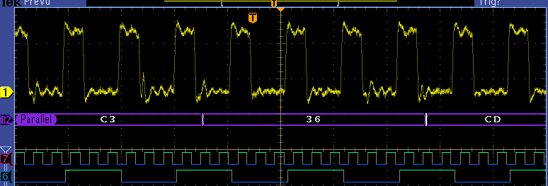
So, on that forum they opened my eyes to some things that for many would seem common truths, but for me it was a surprise. For example, it seemed to me a strange form of the clock signal arriving at the processor with a monstrous "ringing" in amplitude:
It turned out that this very signal looks completely different if you just take the “ground” not where I took it (on the other end of the debugging board, which is more convenient), but directly at the signal receiver (processor):

It’s a trifle, but , in my opinion, it is from such trifles that a true understanding of many processes is formed ...
By the way, about the equipment on which this picture is made. In the course of the fuss with the 86RK, I got a pretty good portable Fluke oscilloscope, but for some reason my soul didn’t go to it right away. Why - I don’t know, not that, and that’s all ... So the new project turned out to be a good reason to purchase a new oscilloscope. Lusting on the idea, sometimes I make hasty decisions. And so it happened this time. Instead of studying the subject in detail, I got the first device I liked - the Tektronix MSO3012. No, I can’t say anything bad about the device, on the contrary - a really convenient interface, a bunch of useful functions, an almost full-fledged 16-channel digital signal analyzer, the ability to view signals in the form of a logical bus, connect to a computer either directly or via a network, etc. .d. I just always want more and one could choose a more modern series - MDO, which also offers a built-in generator of arbitrary signals. And the tool is very cool - I’m envious of those who use such equipment to solve real problems, and not for primitive crafts, as in my case ...
Returning to overheating of the processor, they convinced me at the forum that for this microcircuit, such a temperature is completely normal (just the power consumption is large). I finally calmed down after changing the processor to a one made using more modern technology, and after that it remained completely cold throughout the process.
Having got 8088 with a (potential) bunch of peripherals at my disposal, my hands were completely combed out to program something more complicated than managing a 7-segment indicator. True, the question arose about a normal integrated environment for programming in assembler real mode (the only language I knew). And here I was waiting for a big bummer. If for the 8080 / Z80, as well as for all modern controllers, there are plenty of both free and commercial IDEs with all conceivable and inconceivable gadgets, then for x86 there was nothing decent at all. There were some abandoned amateur projects, and that’s it. There are several reasons for this, but the fact remains. In the end, I settled on WinAsm (the first thing that somehow worked for me), which can hardly be called a full-fledged IDE (primarily, due to the lack of a debugger), but at least something (like compilation directly from the editor) he allowed to do. At that time, I decided to use the old honored Turbo Debugger, launched in DosBox, as a debugger.
First of all, I wanted to get a normal way of displaying information for my device, i.e. video adapter. Although in a heap of places (including on Habré) you can find articles on the topic "How to write a video adapter on HDL yourself in 5 minutes", making my module was simply an unattainable dream for me. Therefore, I climbed into the well-known opencores.org and found there the simplest alphanumeric VGA video adapter, and even on VHDL (most of the projects on opencores are written in Verilog).
Although this module was almost a complete device, nevertheless, some work was needed to work with my debug board (related, first of all, to the specifics of the digital-analogue part of the DE2-115 VGA interface). Armed with my rudimentary knowledge of individual VHDL expressions, as well as (mainly) scientific poking methods and successive approximations, in the end I managed to do something that seemed to meet my needs and compiled without errors.
At this point, I had already started more or less oriented in circuit design, so it wasn’t difficult to convert the video adapter module into a symbol and insert it into my circuit. At first, as a video buffer, I used the ROM generated inside the FPGA with a pre-recorded test message. Pretty quickly, I saw this message on the VGA monitor screen, after which it was possible to change the buffer on RAM. At this moment, the next (and far from the last) time I felt the charm of FPGA. In video adapters, there is always a conflict between the need to continuously read the video buffer to display it on the screen, and the processor's need to write data to the same buffer (and sometimes read it too). The problem is solved in different ways, but, in any case, this is far from the easiest node (at least for me). But with the FPGA, everything became elementary - I just generated a dual-port RAM, which had two sets of address and data buses. The processor, of course, was connected to one port, the video adapter - to the second. What happened there inside the RAM, and how conflicts were removed while accessing the same memory cell at the same time - these were Altera's problems, but not mine at all.
As the main RAM, I used the 16x1M static RAM available on the board (in the sense, 1024K of 16-bit words). The ROM generated inside the FPGA was still used as a ROM - although there is more than enough flash memory on the debug board, it is much more convenient to use the built-in memory for debugging purposes, especially since I did not experience a lack of it.
So, I suddenly had a completely working system on an 8088 processor with a video adapter, a bunch of (relative) memory and a lot of connectors for connecting to anything. All of this was clearly asking to do something else with him.
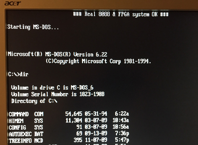
Once again a thought began to appear in my head, which I had stubbornly chased away several times - “Maybe DOS? ..”. And at some point, at the peak of self-confidence, I gave up ... So, we will try to run MS-DOS!
Obviously, to run DOS, I will need to implement the necessary BIOS functions, but what is hidden under the word “necessary”? Basically, I knew where to find the maximum minimum (or minimum maximum?) Of functions - namely, in the first BIOS version for IBM PC. Since all versions of DOS should work on this BIOS already, in any case, it would be possible to limit only to its functions. It was not difficult to find the BIOS source on the Internet, and a quick look showed that there was nothing particularly mysterious there. In fact, I needed to work with the INT 16h keyboard, a 10h video adapter, a 13h drive, and a few other simple functions like returning the amount of available RAM that were implemented in literally a few lines of assembler.
First of all, in the depths of the Internet, a VHDL module for working with a PS / 2 keyboard was found and embedded (all in the same circuit design) into my circuit. It was decided not to bother with the interrupt controller yet, as the keyboard at that moment was planned as the only source of interruptions.
So, we could start writing the INT 09h handler - keyboard interrupts. And then another ambush awaited me. In the life before last, I pretty seriously programmed in x86 assembler, but it was so long ago that almost all the subtleties from my head disappeared completely. No, it’s clear that mov and cmp are hard to forget, but all the more difficult it was with great difficulty. For me there is nothing worse than doing what I already did, and learning something is no exception. Especially if you remember that once you were pretty cool at something, but now you can’t say either no or no ... I had to grit my teeth, download some kind of assembler textbook and read it in express mode.
Naturally, remembering is easier than starting from scratch, but my programs, especially at the beginning, to put it mildly, did not differ in elegance. It’s approximately like trying to retell Shakespeare in English, using a vocabulary of a hundred words and two times ...
Nevertheless, pretty quickly the minimal set of INT 09/16 worked, and after it support was made for several basic functions of INT 10h for displaying characters on the screen . It was possible to start a much more complicated thing - working with the disk.
Naturally, I was not going to support a real hard drive. The idea was to emulate a hard drive through working with an SD card, especially since there was a connector for such a card on the debug board. There were no problems with the disk image - in order not to go far, I took a disk image for the project already mentioned herezet.aluzina.org
With the support of the SD card, two big questions arose immediately - hardware support for the SPI bus and the protocol for interacting with the card itself.
In principle, SPI can be implemented completely programmatically, but I wanted to have fun with the hardware as well, so I heroically set about drawing a byte transceiver in a circuit design. To my surprise, there was nothing complicated about this, and pretty soon I was already observing on the oscilloscope screen briskly running 8-bit packets containing exactly what I wanted. By the way, here I first appreciated the ability of the new oscilloscope to not only show a bunch of signals, but also to combine them logically into the corresponding bus. It is much nicer to see that the oscilloscope realized that it is the A5 byte that is being transmitted, rather than manually watching if the transitions from 0 to 1 and vice versa are in the right places.
With the protocol for communicating with an SD card, it was slightly more complicated, but not by much. On the Internet there is a bunch of resources where everything is carefully chewed, so finding the necessary information was not difficult. In principle, almost everything you need about this in a super-concentrated form can be found here - nada-labs.net/2010/using-the-buspirate-with-a-sd-card
To simplify the task, I did not try to adapt to all types and varieties of cards , but limited to the original SD (not SDHC or some other options) card. A bit of programming, and now the contents of the 0th sector of the map began to be displayed on the screen. Immediately after that, I brought these functions to some kind of INT 13h, added in its infancy INT 19h (boot load) and saw the following on the screen:
Since at that moment only the 0th sector was always read during reading, the bootloader (located just in this sector) did not find the OS to boot, which was reported. But these are trifles - the main thing is that my circuit slowly began to turn into a real computer and even tried to boot!
Next came the struggle with the conversion of physical sectors into logical blocks. Here I also acted up and, instead of defining the parameters (image) of the disk, I simply hard-coded the numbers for a specific instance of the image. I had to tinker with this part - for some reason, calculations led to completely unexpected results (I never liked assembler arithmetic at all). Nevertheless, after some torment, the physical sectors / cylinders / heads began to be correctly translated into logical blocks, and it was time to try to boot already seriously.
Naturally, the download did not go right away, and I did not expect this. Knowing in advance that I didn’t have a lot of functions in the BIOS, I put stubs on all interrupts, and when I accessed an unrealized function, all the necessary information was displayed on the screen — which interrupt and which arguments are being addressed. Next was the process of writing a handler for the corresponding function (and even more often - just a temporary stub), and the process continued. Suddenly, everything stopped at a function that is completely absent in the original PC - one of the INT 2F functions related to event processing. I saw that DOS determines the type of PC, and it should not cause interrupts that are absent on this type, but, nevertheless, this happened, and the process stopped. A simple stub did not help, but I did not want to implement the entire function from the principle.
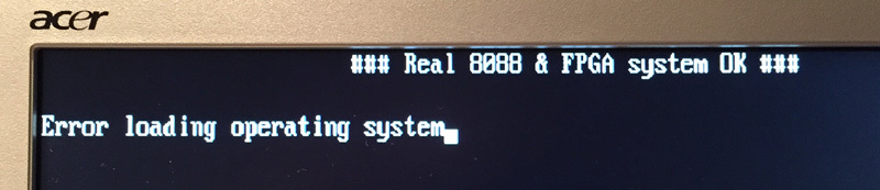
Now I don’t remember the whole train of thought (I looked at a lot of things at that moment in the DOS sources and during the boot process), but once again on this “freeze” I decided to call a bunch of interrupts (at that moment I had the timer off on INT 08h ) and pressed the Shift key. Suddenly, a miracle happened:
Frankly, quite a lot of emotions came over me - to go from a breadboard with a couple of chips to loading DOS in a month, and even with short raids (due to a chronic lack of time), it seems pretty cool (sorry for showing off)!
By the way, with this message I still have an unsolved mystery. The fact is that after finishing the timer interrupt, DOS began to load without freezing in this place, but for some reason, the Microsoft copyright message is not displayed. It seems that it is also not displayed on a real computer (unfortunately, there is nothing to try). What is the root cause - a mystery covered in darkness. I tried to understand the logic of the DOS source code, but I didn’t see it right away and didn’t want to spend a lot of time. Nevertheless, the question is still tormenting slowly ...
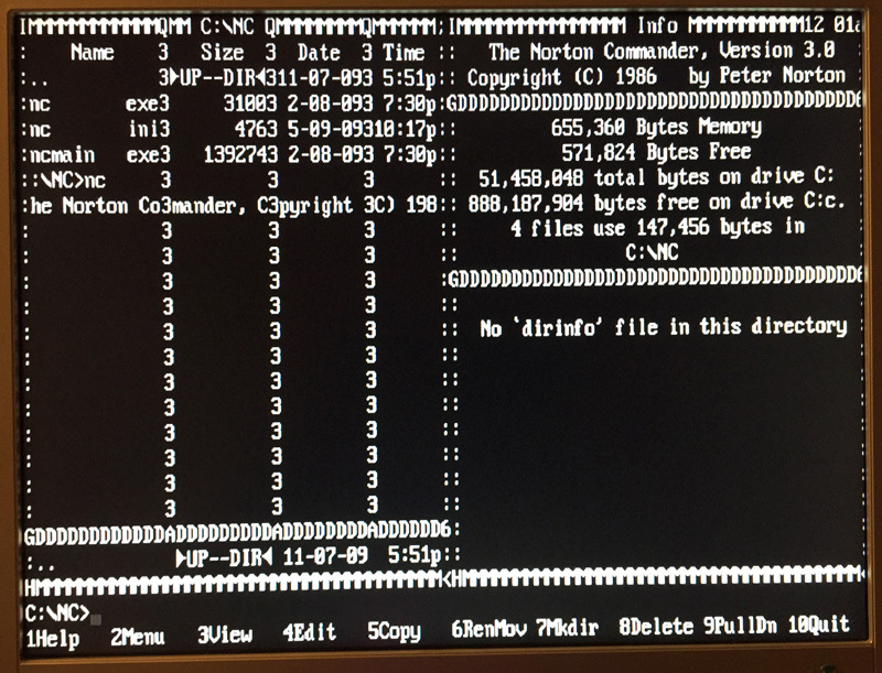
After starting DOS, it was the turn to start other programs. You can probably guess whose turn was first - naturally, as they say, the good old Norton Commander. Oddly enough, the fuss with him was noticeably more than with DOS. NC at startup caused a wild number of functions, and in some cases it was not possible to manage with simple stubs, I had to write at least a minimum of functionality.
Nevertheless, the problems were more quantitative than qualitative, and soon managed to bring the NC boot process to its logical conclusion:
This “interesting” appearance was due to several reasons:
- the video adapter did not support attributes at that time
- I did not have the second part of the character generator, which contained the pseudographics, so the characters from the bottom of the code table turned out to be in the appropriate places
- some INT 10h functions were not implemented.
In general, I was periodically surprised at how exactly certain functions were implemented in various programs (and even in DOS). For example, the CLS (clear screen) command called the INT 10h function, causing the window to shift up. In this case, the entire available screen area was indicated as a window, and it was shifted by the number of lines equal to the number of lines on the screen. Since I did not expect that someone uses the windowing functions at all, I was in no hurry to implement them. The result was obvious (or rather, on the screen). However, we will return to the oddities of some programs a little further ...
After launching NC, I had a natural desire to bring it into a divine form. Moreover, such a part of the work is sometimes even more enjoyable than trying to get a dead device. There were no special problems with pseudo-graphics - just quite a lot of time for manual drawing of characters (I had a character generator directly in the form of VHDL code). But with the attributes I had to strain a little.
Even earlier, during the process, I began to apply some elements of VHDL. At first it was almost violent - after all, there was a desire to try to learn this language again, and then because in certain cases it turned out to be more convenient than using a circuit design. Even in the video adapter itself, I had to delve into the code - initially 43 (or something near this) lines were supported, but I had to redo 25 lines. And at first I tried to make attribute support a circuit design, but suddenly I began to realize that it might be easier to use VHDL for this. Naturally, everything moved with great difficulty and using the simplest language constructs, but I suddenly began to understand the essence of VHDL - still just a little bit, but enough to start consciously creating something on it, and not just modifying the existing one.
My fuss with VHDL was not in vain, and after a while I was able to see something familiar for a long time:
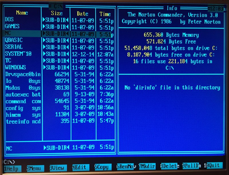
Yes, there were still some imperfections (such as an attribute shifted by one character), but overall the 80x25 color text mode worked like this as it should.
Next in line was the interrupt controller 8259. At first there was an idea to try to use an existing one from some project, but I didn’t like any of them for various reasons (either they were too primitive, or, on the contrary, I didn’t understand how they work, but no documentation). There was even an attempt to buy a commercial IP (in this case, IP is not the Internet Protocol, but the Intellectual Property), but the manufacturers did not want to bother selling one whole thing ...
In the end, I had to take up a piece of paper and sketch out something like (block) the controller circuit, which I then began to implement on VHDL. I did not pursue full compatibility - I needed (at this stage) support for one main mode of priority interrupts, the ability to mask interrupts (also read the interrupt mask) and execute the EOI (End Of Interrupt) command. In my opinion, this should be enough for the vast majority of programs to work normally with this. Looking ahead, I’ll say that to this day I haven’t found a single program that would try to do something beyond the functionality I had built with the interrupt controller.
Probably the interrupt controller was my first real (albeit small) project on VHDL - from start to finish. I wrote it carefully, I was not too lazy even (again for the first time in my life) to make a test bench (not sure how to correctly translate into Russian - in fact, a sequence of signals to verify the correct functioning of the device). The simulation in the ModelSim simulator showed the controller to be fully operational, after which another graphic symbol was generated from it and added to my device.
I did not have a normal timer 8254 yet, I used a regular counter to generate 18.2 Hz interrupts, which I connected to the interrupt controller. The behavior of the computer showed that everything seems to work - DOS booted up without having to press a button, and finally the clock went to NC. It seemed that the next stage had been passed, and you can safely move on.
As it turned out, I was happy early - at that moment, perhaps the biggest problem in the entire project was discovered. If anyone remembers, the NC has a built-in screen saver - "starry sky". Leaving my computer for a while, after returning to it, I found that the stars on the screen saver froze for some reason, in other words, the computer was frozen. Although I understand that such accidents do not happen, I still wanted to believe in a miracle - that this is an isolated case. Unfortunately, as always, a miracle did not happen - after a complete reset and reboot, the computer freezes again after an hour or so of work. It became unambiguously clear that somewhere there is a problem, and it is very difficult to find.
To narrow my search as much as possible, I wrote a simple memory test that ran immediately after a processor reset, without initializing all unnecessary devices such as a timer, etc. In principle, I took the indication of a memory error with relief - at least the problem was clearly in the hardware. The only thing left is to understand in which particular place. And this turned out to be not easy at all.
The fact is that, in general, the circuit involved in the process of testing memory is, in its essence, quite primitive. A minimum of logic is involved, except for the processor there are no other complex programmable elements. As a result, after some time spent analyzing the circuitry, I had more or less confidence that the problem was not a fundamental error in the circuit, but something more random - for example, interference.
With this side of circuitry, in general, everything was bad for me. I knew that more blocking capacitors needed to be installed, and that long wires were kind of bad. On this my knowledge ended. Therefore, for advice, I again turned to one of the professional forums. I was given a lot of advice, sometimes it was difficult to separate really sensible advice from the advice on the principle of "I will say everything that I know at least a little on this subject." I will not describe all this here - too much has been discussed, so this may be the topic of a separate article. According to the results of discussions, my motherboard has grown with almost two dozen blocking capacitors and completely lost its original more or less glamorous look.
Unfortunately, the next test run showed that the problem did not go away. Perhaps it began to appear a little less often, but it’s hard to say - and before, a failure could occur in 20-30 minutes or in a few hours. Now, at least, the board left overnight in the morning turned out to be guaranteed to fail. In desperation, I again returned to the analysis of circuitry and an even more careful study of the processor bus diagrams. In one place I had a certain thought, and again I went to the same forum. During the discussion of my idea, I once again received a portion of useful (and sometimes not very) tips, tried to implement some things (primarily related to the slight delay of some control signals), but this did not affect the presence of failures at all.
At the end of the road, a concrete dead end clearly loomed, so I began to check crazy ideas in general. In particular, will the memory chip itself fail? For verification, I generated a RAM module directly inside the FPGA, which I used instead of external memory. Honestly, I did not hope for the result - I just did everything that came to my mind. But imagine my surprise when after that the failures suddenly disappeared! In general, I was somehow not even ready for this, so I did not quite understand how to use this knowledge. The fact that the memory chip is faulty was not believed even at this moment. There was also almost complete certainty that I was working with this microcircuit correctly - according to the control signals, everything was as simple as that. But the fact remained - with the microcircuit, the failure was guaranteed to occur no later than after a few hours of the test,
To clear my conscience, I decided to test the memory with a completely different circuit, without using my processor board. In the process of thinking about how to do this, I suddenly had the thought - I understood the only significant difference between using internal and external memory. The fact is that the external memory was asynchronous, and the internal one was partially synchronous, and for it an additional signal was required, by which the address of the cell that was being accessed was latched in the internal buffer.
I did not understand at all how this might relate to the problem of random failures - it was completely clear from all the diagrams that my address was holding much more than the minimum necessary for memory, therefore, theoretically, this could not be the reason. Nevertheless, I immediately drew another register in Quartus, filed an address on it and snapped it with the same signal that was used for internal memory. The output of the register, of course, applied to the address lines of external memory. Realizing that I was doing complete nonsense, I ran a test. And the test worked successfully until I turned it off the next day. Then, a couple more times with and without a register - it was clearly seen that the presence of a register eliminates failures completely.
This was completely inexplicable - even on the oscilloscope I saw that the address signals already hold on more than this may be necessary in principle, but the fact remained. After the whole weekend showdown, I spat on it and decided to come to terms with it as a given ...
So, DOS was loaded, many programs that did not require a graphics mode started, it was possible to move on. Naturally, there was a desire to launch some kind of toy. But for a toy, as a rule, graphics are required, but I haven’t had one yet. And if for a text video adapter it was possible to get by with a little blood by remaking an existing one, then for graphics this was not so simple.
It was not even the lack of ready-made solutions. The problem was that I needed almost complete compatibility with the standard video adapter at the hardware level - after all, all games work with graphics directly with hardware, without using the BIOS. I realized that it’s easier to make a video adapter “from scratch” than to try to remake some ready-made one. And, of course, it was much more interesting to do it myself.
So, we are writing our own CGA adapter - even EGA is a couple of orders of magnitude more complicated, so for now we will not swing it. In principle, a little to begin with, I nevertheless peeped - I found, in fact, drafts of the VGA scan generation module. But it was a dozen and a half lines, and even not fully working. So, really, they were used as a template for the beginning of scribble - morally it was easier.
Naturally, I didn’t have a CGA monitor and I didn’t plan it, so the idea was to use the VGA 640x400 mode, which perfectly fit the 320x4200 CGA mode by simply duplicating the dots both horizontally and vertically.
In general, the graphics adapter turned out to be unexpectedly easy for me - the brain at this point suddenly learned to think in terms of VHDL, plus a little understanding appeared of what can be required from VHDL and what is not worth it. In general, it took me most of the debugging time to search for a completely stupid error related to bit depth (two such problems overlapped and gave a very funny option). For the rest, I began to enjoy how the lines in the editor turn into almost real hardware inside the FPGA and do exactly what I want.
At the very beginning, of course, the adapter turned out to be far from perfect and compatible, but Checkit was able to recognize it and even display the first test picture:
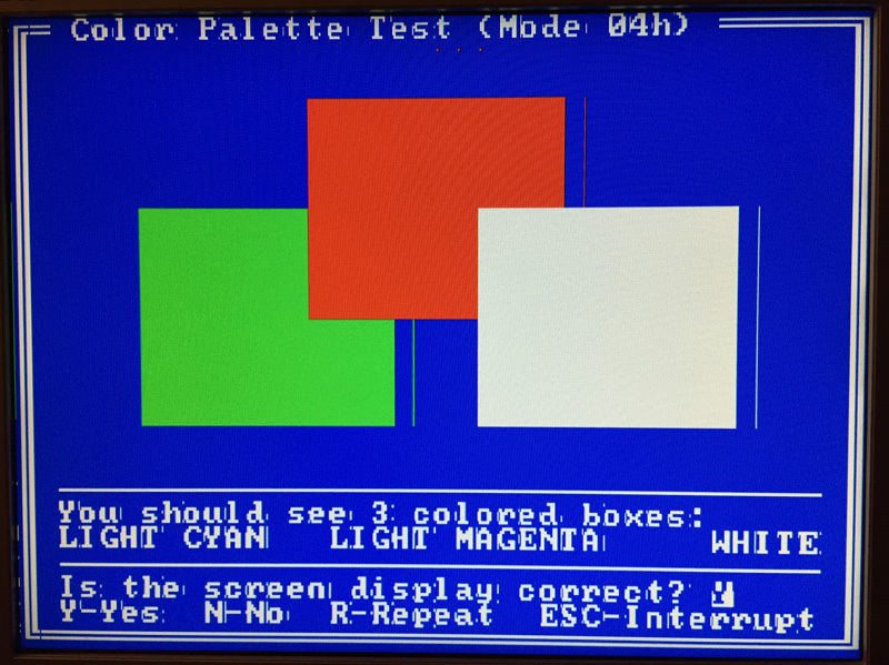
By the way, Checkit turned out to be a rather useful program - he defined many things in rather tricky ways, which made the whole design more and more PC -compatible. And since Checkit could check all nodes and components, compatibility was also tested for all parts of the system.
After fixing the most obvious mistakes (such as duplicating a point from the previous byte visible in the previous photo), it was possible, with some difficulty, to find a game that seemed to work:
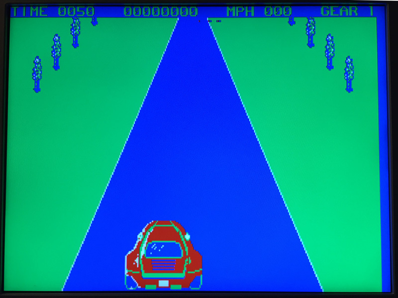
The colors in this picture do not correspond to the original ones - at that moment the switching of the palettes has not yet been done, yes and the colors themselves were not tuned at all.
Attempts to find working games have shown that gaming programs, in most cases working directly with hardware, are much more demanding for compatibility than any NC or even QuickBasic. Fortunately, FPGA provided almost unlimited possibilities for revealing the facts of the program accessing the ports of interest, memory addresses, etc. Especially with the fact that I could also change the BIOS at my own discretion, this provided an excellent debugging mechanism. By the way, at some point (I don’t remember exactly when), Turbo Debugger started working, which also expanded the arsenal of debugging tools.
It immediately became clear that at least a minimum timer of 8253 had to be done. Moreover, the programs tried to use the timer not only for sounds (channel 2), but also actively reprogrammed channel 0, thus changing the frequency of interruptions from the timer, and also used this channel to determination of time parameters.
After reading the documentation for 8253, I felt a little sad. It was necessary to do a lot and not very interesting. Having decided to do this somehow later, at that moment he just climbed onto the same opencores and pulled off a couple of timer modules. One on Verilog, and very simplified, the second - in appearance extremely sophisticated, and even on VHDL. Unfortunately, the timer on VHDL was connected via the Wishbone bus - this is an open standard for FPGA development. I had never encountered Wishbone before, so I decided to start using the module on Verilog, which looked simpler on the interface.
After connecting the timer to my system rather painlessly, I conducted several simple tests and made sure that the module seemed to work. Not only that, after another minor revision of the system, the first but quite correct sounds from a working toy were heard in terms of the interface with the speaker. So far, with a timer, you could finish and move on.
Then I had to make a radical decision. Until now, I wrote INT 10h myself. In text mode, one could still come to terms with this, but the need to support these functions in graphic modes upset me. Considering that by this moment the passion for assembler programming was almost satisfied (nevertheless, it was felt that I had to do it in industrial volumes at one time), I acted on the principle “If the mountain does not go to Muhammad, then he sends it nafig ". Namely, he decided to make his CGA adapter so compatible in hardware that the original BIOS could work with it.
In principle, there wasn’t much complexity - there are not very many registers, their functionality is extremely simple. Of the implicit things - I had to emulate a state register in which there are signs of a reverse beam of a vertical and horizontal scanning. It turned out quite logical that many programs (including the BIOS) actively use this register to avoid "snow" when trying to access the video memory from the processor and adapter at the same time.
For some reason, the process of putting the video adapter in order seemed very exciting to me, and in the end this node turned out to be the most elaborated in terms of compatibility with the original device. Along the way, missing things were added such as switchable palettes, 640x200 mode, etc. By the way, for testing the 640x200 mode, it turned out to be rather difficult to find a program that supports this mode. The only thing that I managed to dig up was chess:
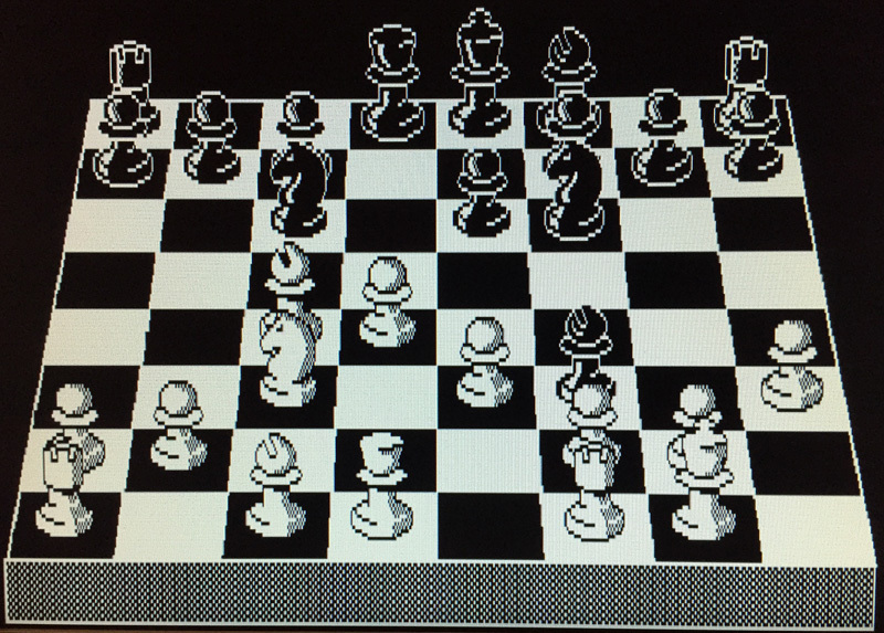
In my opinion, it looks pretty nice ...
The original INT 10h handler was very friendly to such an adapter, and I breathed a sigh of relief from not having to write things like character recognition printed in a certain place on the screen in graphic mode .
The last hurdle to acceptable PC compatibility was, oddly enough, the keyboard. Although this was almost the first thing I screwed on the project, but from the point of view of compatibility there was still no horse lying around. The main problem was that all normal programs work with the first set of scan codes that was used by IBM PC. But all keyboards, starting with PC AT, give out at least a second set of scan codes, very different from the first. Only the keyboard controller inside the computer converts these codes into the original, first set, and all ordinary programs work with it (even if these programs seem to access the keyboard directly without using the BIOS). Naturally, I didn’t have any controller (by the way, PC AT and even later PC XT used a separate microcontroller based on 8051). The functions of INT 09/16 were implemented in my most minimal form, and there was no question of direct operation of programs with a keyboard in general - they (programs) simply would not have understood a single scan code.
At this point, I suddenly felt euphoric from owning VHDL - it seemed to me that I had already comprehended the truth, and I can do anything. Therefore, without delay, an elegant (as it seemed to me) module was written on VHDL, which performed the conversion of scan codes. Everything was very beautiful and good in this module, except for one small detail - it did not work. Moreover, I could not understand the reason for the inoperability in any way, which was frustrating and puzzling - there were only a dozen lines there.
Once again, turning to the forum for experts, I received a fair amount of really sensible advice. Not only that, my understanding of the VHDL concept itself once again almost changed radically (including, some disappointment appeared). The main thing - there are no miracles. VHDL (as well as all other HDLs) will not do what cannot be done in the usual way from the available hardware resources. If I write a line that seems to be correct from the point of view of the language syntax, but at the same time I can’t even imagine how this can be implemented in hardware, then most likely it will not be implemented during compilation. At a minimum, it will not do what is required of it. And yet - it is very important to use templates. It turns out that many language constructs turn into the correct hardware nodes only when the compiler recognizes the corresponding template.
I think that it was after these showdowns that I really, at least a little bit, really started to understand the essence of VHDL (and Verilog also ceased to be completely incomprehensible at this point). Magically, the textbooks in these languages suddenly made sense, and behind the words the essence of the things described became clear.
In short, by making the converter module a little less beautiful, but much more correct, I received codes in the first set at its output. Then it remains to feed these codes to the original INT 09h handler, and check with the same Checkit for the correct recognition of keystrokes. So, the keyboard was also almost 100% hardware compatible.
At this point, I began to feel more and more inconvenience from the fact that I still had the circuit design as the top level of the project. The final impetus, prompted to take up the full transition to VHDL, was the change of home computer. On the table, I had an iMac Retina with Windows installed. Unfortunately, Quartus was among the programs that were completely unprepared to work with such a screen resolution. The circuit design became completely unreadable, and my attempts to adjust something did not bring any real improvements. There was nowhere to go, I gritted my teeth and took on a text editor.
Oddly enough, everything went more than smoothly. Now I don’t even remember if it was necessary to debug at least something, or if everything worked right after the alteration. In any case, there were definitely no serious plugs, but working immediately became much more convenient and efficient. I immediately remembered the advice of a number of knowledgeable people who strongly recommended that I forget about the circuit design from the very beginning and immediately start with VHDL / Verilog. By the way, regarding VHDL vs Verilog - please do not argue with me which is better / worse, and why I settled on VHDL. Let's assume that I just wanted to, and this is almost true. More on this subject I will not argue ...
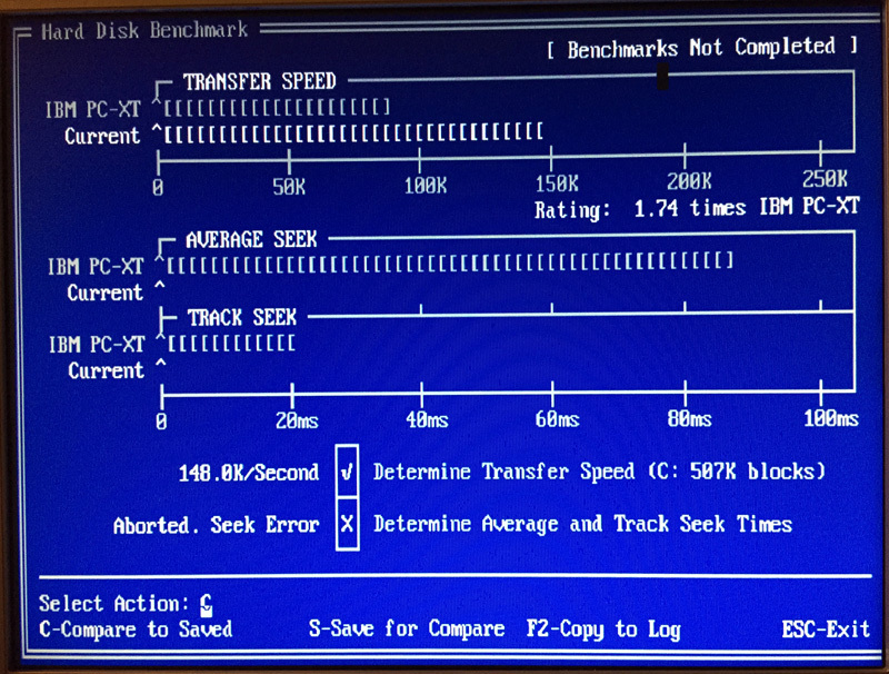
When switching to VHDL, the last module on the circuit design, the SPI interface, was also completely redone. If you remember, it provided hardware reception / transmission of only one byte, and around this it was necessary to carry out a number of preparatory steps. Coupled with a slow processor (and lazily written by INT 13h), this provided only about 35% of the speed of the original PC XT hard drive (according to Checkit). Since I almost felt like a guru of VHDL and digital electronics in general, I immediately decided to write not a copy of the existing interface, but a module that provides packet transmission.
True, I decided not to bother with DMA (or, as we say in Russia in Russia, PDA) - there was no DMA controller yet, but I didn’t want to take on two new modules at once, then you won’t figure out exactly where the problem is. Debugging the module did not go quite smoothly - I had to tinker a bit, including actively using the digital channels of the oscilloscope as a protocol analyzer. By the way, for some reason, during the whole process, I almost forgot that Quartus includes a built-in digital SignalTap analyzer, which, probably, would be even more convenient. Perhaps in the future my hands will reach him (I have never used one before), but so far I really like to use a separate piece of iron for this.
Probably, taking into account the new module, it would be possible to rewrite INT 13h more seriously, but I was too lazy, and I got off with only the minimum necessary modification. The result was a not very beautiful and completely ineffective pile up, but still the speed with the new module increased almost 5 times:
Next came the partially tedious, partially fascinating process of launching various programs (primarily gaming) in order to find out why they do not work (or rather, that my computer is not compatible enough). You can write a separate large article about the search for reasons, I will just give a few examples:
- I do not have DMA. It turned out that the zero channel DMA (used to regenerate memory on the original PC) is also used by some programs as a counter to determine short time intervals. I had to emulate the corresponding part of the counters of the DMA controller
- usually (but not always) when reading from a nonexistent memory area or I / O port, the FF byte is read. I read the opposite - 00. I did not like the program, which checked in this way (and nothing more) the presence of a joystick, after which it decided that it was there and that all the buttons were clamped
- the most original way to determine the presence of a CGA adapter was used by a program that wrote a certain value to the cursor location register, then read the value and checked against what it was recording (then restored the original value). According to the documentation I have, this register seems to be only for writing, but redid for reading / writing, after which the program calmed down
- not related to my computer - spent a lot of time figuring out the reasons for the freezing of the simplest ancient game Paratrooper. It turned out that although the game is old, the file I had was compressed by a self-extracting com / exe file archiver. So, the part that was then responsible for unpacking the program at startup contained a command that appeared only starting from 286 processors. The trouble was that this command did not greatly affect the unpacking process and spoiled only some bytes (less than one out of a thousand). Perhaps, I spent the most time on these disassemblies.
So, slowly, almost all the games that I had began to start and work without any problems, I even tried to play some of them:
During the launch of numerous games, it turned out that my timer module was far from ideal - in most cases the sounds were not entirely correct. Having decided that I still want to deal with the Wishbone bus, I decided to fasten the timer on VHDL, which I mentioned earlier. To begin with, I read the description of Wishbone and piled something like an adapter between the Wishbone interface and the 8088 bus - nothing complicated. Unfortunately, the timer did not work. I had to get the oscilloscope again and see what was happening there (first of all, if the Wishbone signals were formed correctly).
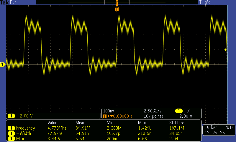
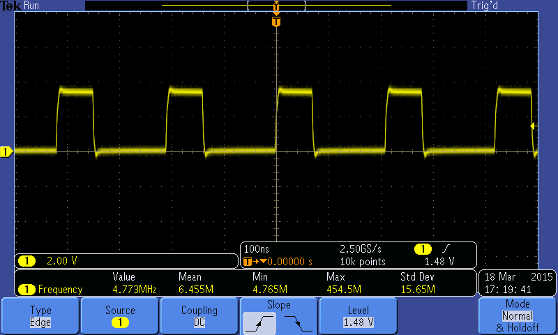
Who would have thought that at this moment a great discovery would be waiting for me ... Remember how I was tormented with memory failures, and had to enter an intermediate register, which I did not see the need in principle? So, on the oscilloscope screen, I had the following picture:
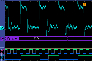
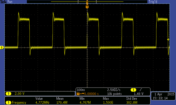
Naturally, the first thing that caught my eye was the terrible ringing of signal 2. Moreover, this ringing passed from a quantitative parameter to a qualitative one. Signal 6 is generated by a single-bit counter, to the input of which signal 2 is applied. In fact, on each rising edge of signal 2, signal 6 is inverted. But the waveform shows that signal 6 switched once not only along the normal edge of signal 2, but along the edge of the strongest “ringing"! Those. in my circuit, on some lines the ringing was of such amplitude that it could cause false switching of logic. To say that I'm freaking out is to say nothing. I could not even believe that with all this I was able to achieve stable operation of the circuit ...
Further, after a little analysis of the circuit taking into account the new data, it became completely clear to me exactly where the old failures occurred, and why that register cured them. Nevertheless, it was necessary to do something, since it was signal 2 that I needed to work with the new timer module. And again, the traditional appeal to connoisseurs. Of the several tips on the forum, the option was chosen with cutting the track and soldering the resistor there. The result was far from ideal, but I did not record more false switching from ringing during testing for several hours:
Unfortunately, this did not affect the performance of the VHDL timer module - it was silent. Having tinkered for some more time, the reason was discovered in a rather unexpected place - in the module itself. Moreover, it was quite prosaic (and often found in programming) - the module incorrectly processed one of the extreme values, namely, with a divisor of 0, instead of dividing by the maximum value (65536), it did nothing. I checked all the time exactly the initialization of channel 0, which is initialized by the maximum divider to get a frequency of 18.2 Hz. When I used the FFFF divider for the experiment, it worked.
I even contacted the author of the module, which (the author) had already forgotten that he wrote this module. Nevertheless, the author helped me find a specific place where a mistake was made, and I even somehow tried to correct the mistake. It was this problem that was solved, but others were discovered, so for now I settled on the first version of the module, on Verilog.
At this point, the readiness of my design was such that I was ripe for the main experiment. The fact is that back in '86 I read an article from the magazine 'In the world of science', which is a Russian translation of the American journal Scientific American, which talked about the latest Microsoft product - namely, the game MS Flight Simulator. Considering that already at that time I was a fan of computers, but at the same time I was determined to become a pilot, we can understand what emotions were seething in my head (and in other parts of the body).
And now, after almost 30 years, I had an unquenchable desire to launch exactly that historical Flight Simulator on my computer. The interest was also fueled by the fact that, in those days, it seemed that two programs were almost officially used for compatibility testing - the very Flight Simulator, as well as Lotus 1-2-3. It was said that they use the hardware features of the computer so tightly that if these programs work, then everything else will work even more so.
In general, I had some doubts - I still knew about some of the pitfalls in my design, but still decided to take a chance (especially considering that I naturally didn’t risk anything). Result on the screen:

By the way, the mysterious graininess of the picture at first aroused my suspicion - I immediately began to think about some completely tricky way of working with a video adapter that I do not have. In fact, as it turned out, in this way Microsoft tried to get additional colors by combining dots from the available colors. I must say that, given the resolution of 320x200, the result was, to put it mildly, dubious.
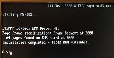
There were no problems launching Lotus 1-2-3 either, so the experiment could be considered finished. Nevertheless, I carried out a number of small tweaks and twists, after which all the programs that I have at the moment started to run and work absolutely normally. The only new feature I added after this was EMS. I just wondered that more than a megabyte of available memory was missing (to be honest, I just wanted to do something else), so I found a description of the EMS board with the driver, and wrote a module that emulated the operation of this board. The driver successfully recognized the memory:
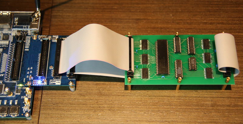
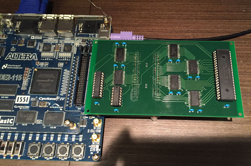
The final touch was the redesign of the processor board itself. I absolutely did not like the nightmare that was happening with the waveform, and I also wanted to practice with Eagle again. As a result, a 4-layer printed circuit board was divorced, in which one of the inner layers was allocated underground, the second - for both supply voltages. In addition, the most significant point was the elimination of the loops - the connectors were installed so that my board plugs directly into the FPGA debugging board (to be absolutely precise, then the FPIO debugging board's GPIO port expansion card is such a nesting doll):
There were also some circuit changes - the 8284 clock generator was completely removed (I decided that it could be easily removed inside the FPGA without causing the slightest damage to compatibility on the bus signals) and the latch register on the address / data bus (also removed inside the FPGA). A quick check of the waveform on the new board showed that the signals became almost perfect:
So, the path from a flashing LED on a solderless breadboard to a completely normal computer was covered in a couple of months, and a huge amount of pleasure was obtained, as well as knowledge in a number of areas. The result was a computer with pretty good compatibility with the IBM PC, on which all the programs that I was not too lazy to get worked on without comment, including and those that are considered extremely demanding on hardware compatibility. On the computer, almost completely (with the exception of the INT 13h processor), the BIOS version 3 from IBM PC is used.
As for the project budget, it is almost impossible to say something definite. To begin with, there are only a few microcircuits to include (assuming that the installation can be done with MGTF, the FPGA board and configuration tools, and so on), or everything, from the over-urgent production of boards, the purchase of an FPGA debug board specifically for this project , and ending with not the cheapest oscilloscope?
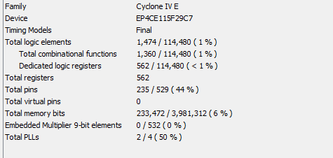
I kind of indicated specific types of microcircuits and everything else in the article, so anyone can see what all this will cost in its version. Naturally, it is not necessary to use exactly DE2-115, for reference I bring the required FPGA resources:
It should be noted that there are still a bunch of artifacts used for debugging, and the code itself was practically not optimized.
What to do with all this (and whether to do anything at all) is not entirely sure. During the process, it once again became clear that, although you can also achieve something with enthusiasm and erudition, a formal knowledge of the basics would make it possible to speed things up, avoid many rakes, and most importantly, concentrate more on creativity, rather than inventing a bicycle with square wheels. Therefore, while there is a great desire to fill in some kind of express method, gaps (or rather, gaping holes) in the knowledge of just the basics of electronics and circuitry in general, and VHDL in particular. How much this will turn out, we will see - there is always a problem in motivation and the availability of free time.