Gikporn 5 or why open microcircuits
Guessed the author by name? But no, unlike the BarsMonster, we will not open the chip out of sporting interest or even to see how it works. We will look for why it does not work. Sometimes this happens, especially if the technology for manufacturing crystals is under development and projects that can be launched can only be experimental. And a similar trouble happened with us. In our case, the obtained samples turned out to be inoperative (the yield is close to zero). A study of the functioning and electrical parameters pointed to the technological problems of manufacturing crystals, which we have yet to discover.
The microcircuit is made according to the technology of 180 nm. With special features that allow digital logic with a high density and a typical 1.8V power supply and an analog component with operating voltages up to 200V to be placed on a single chip. And in conjunction with operating temperatures up to 150-170С makes this technology very popular in industrial and automotive electronics.
To begin with, we carried out layer-by-layer etching of crystals with stopping and full photographing at each technological level. The level of the sixth metal is MET6 (some elements of the photographs are hidden).
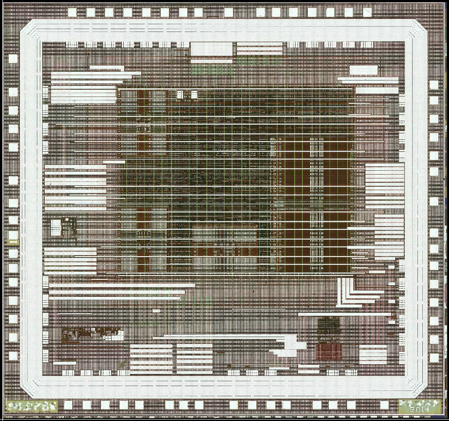
Fifth metal level MET5:
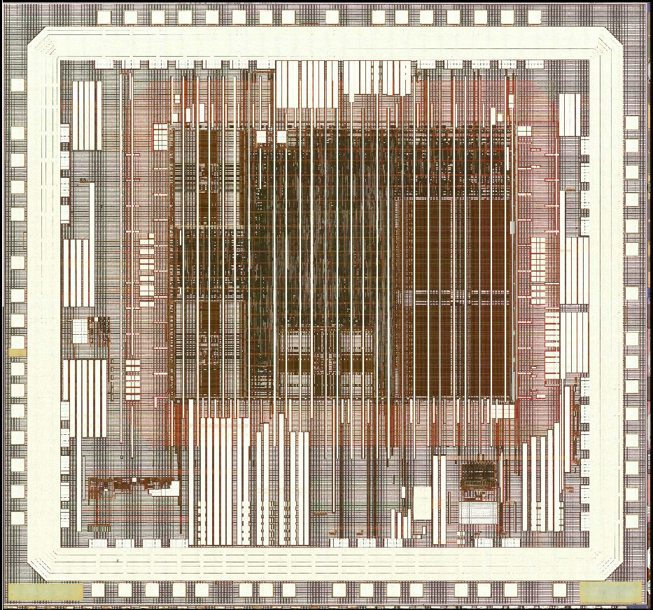
Jumper level between the fifth and fourth metals VIA4:
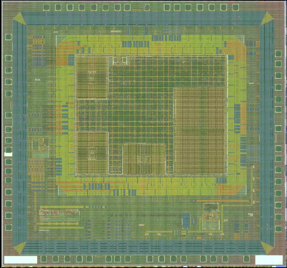
Well and so on, in total we got about 5 GB of photos.
Unfortunately, even very accurate layer-by-layer etching causes various destruction of crystal structures. And to determine that this is a technological marriage of production or the result of the preparation is very difficult. Usually, the criterion is repeatability, if the effects are similar on several samples, then these are technological problems, if the effects are unique for each test sample, then this is the result of the preparation. For example, defects were found in the area of the nutrition rings. At the level of the sixth metal they are not visible, but starting from the fifth metal they began to appear:
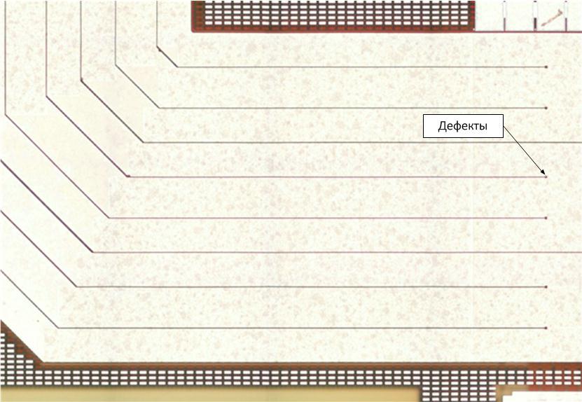
At the level of jumpers between the fifth and fourth metals they became even more
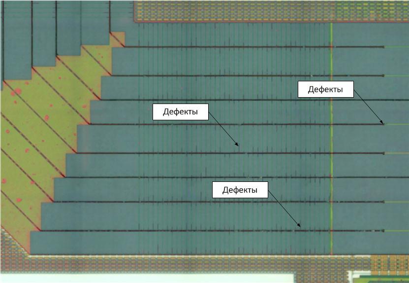
visible : At the level of the third metal they are already clearly visible:
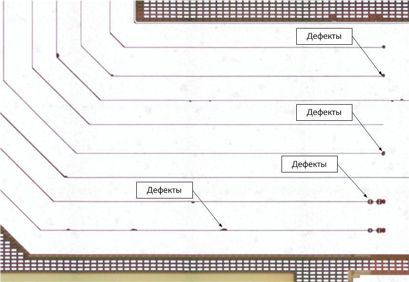
But the defects are unique for each sample and so far are attributed to the problems of the etching process
Missing or incompletely formed vias were found at the bridges between polysilicon and the first metal, unfortunately the resolution of the optical microscope is already at the limit and they are visible as dark spots:
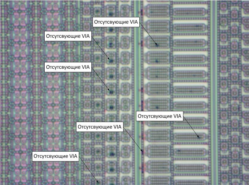
These defects with large correlations were repeated on several samples:
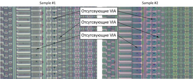
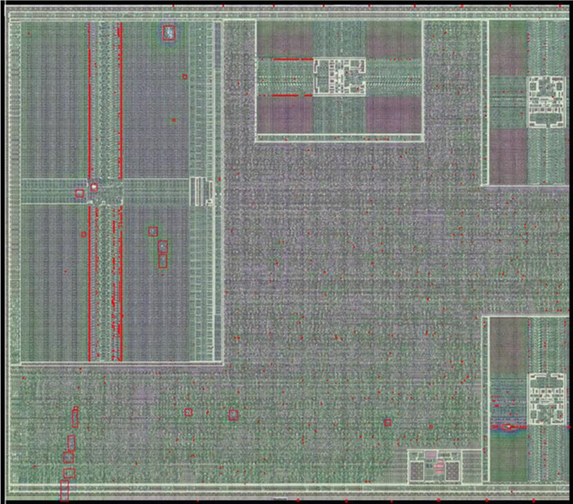
There were a lot of such defects on the crystal flying out "vias, mainly they were in the area of the digital core and memory blocks. In the following figure, they are marked with red dots, red rectangles indicate areas damaged during etching:
As noted earlier, optical microscopy does not allow us to visually assess the condition, and we had to use an electron microscope, and where the electron microscope is, it’s not far from the FIB (Focused Ions Beam) installation. FIB allows a directional ion beam to cut crystal elements with nanometer accuracy or, on the contrary, apply new layers to it, for example, connect adjacent conductors.
We performed a crystal cut in the region where the intensity of the “flying out” VIA was maximum:

And it seems that they found a problem, indeed there was no corresponding VIA on the slice (in this technical process they are designated as CONT). But technologists and topologists of the circuit expressed doubt that we were in the right place. So the remarks of the technologists boiled down to the fact that there should have been at least something, and there was a clean insulator. And topologists pointed out that although the slice is very similar to the topology, it differs from it. In particular, in the topology drawing, the transitional VIA1 and CONT are not coaxial, but on the cut they are located strictly one above the other, and this cannot be attributed to technological spread.
In a more detailed analysis, it was found that this region is really in the same region, but with an indent of about 2 μm, which is completely suitable for this section and it really does not have this transition between the first metal and polysilicon. We just got there.
With the repeated cut, we were able to get to the required area, and there were no more complaints about the transition windows:
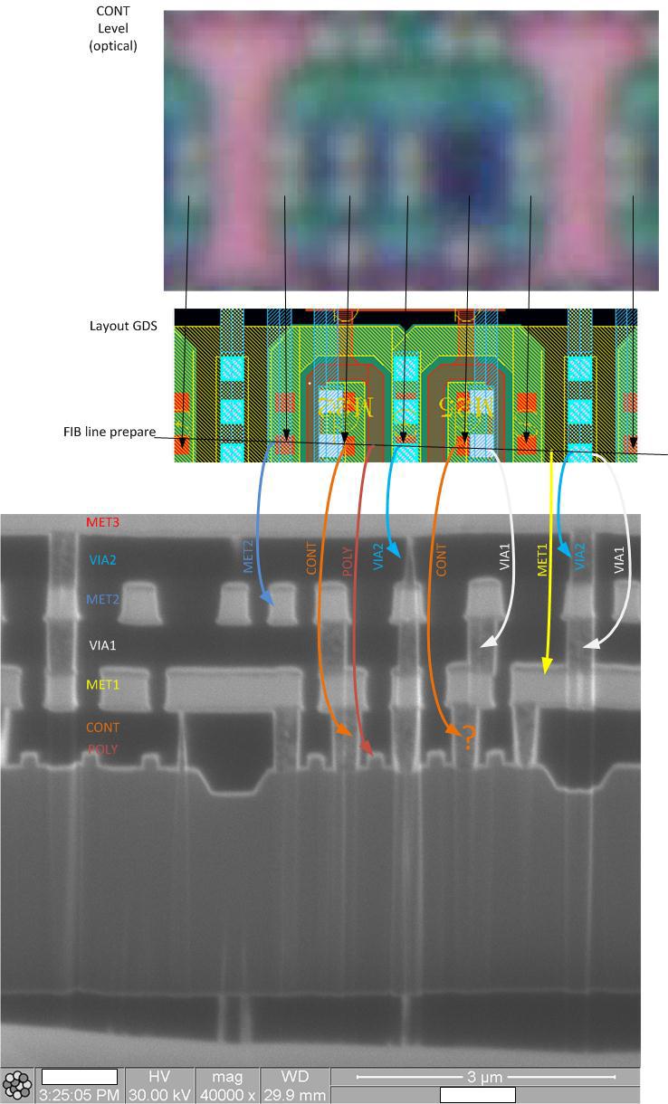
As you can see, now the whole photograph of the slice completely repeats the topology and the VIA between the different layers are spaced. All vias are fully formed. And the reason for the inoperability of the crystals was not found.
When viewing through the electron microscope the level of polysilicon (indicated by POLY), it was noted that in the field of separation of P-channel and N-channel transistors using a deep dielectric (indicated in the DTI figures), polysilicon has some thickening.
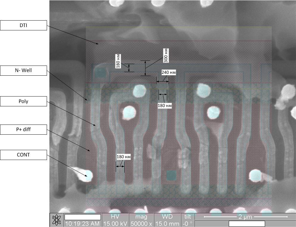
For clarity, a topology drawing is applied to the photo. But at the same time, any gaps or shorts between the various polysilicon tires are not visible. But in any case, we decided to see what is happening there with polysilicon.
But first, let's understand what polysilicon (POLY) is and why it is needed. Polysilicon compounds are a trace resource of the lowest crystal level. The main compounds in the crystal are provided through the metals of the upper layers. But neighboring transistors of one valve can be connected using polysilicon. In order for polysilicon to become electrically conductive it is alloyed (by adding impurities of fluorine, boron or arsenic), sometimes all polysilicon in the crystal is doped, sometimes not. In the case when polysilicon is not doped, its conductivity is achieved by applying a layer of silicide over it (this is a compound of silicon with metals). So in our case, the conductivity of polysilicon over the deep dielectric region (DTI) is achieved by applying a layer of silicide (SiCo2) on it .
For this, we made another cut, which allows us to see the structure of polysilicon over deep and shallow dielectrics.

Already in this photo you can see that above the polysilicon, which is located to the right of the DTI, a white "cap" of silicide is visible, and above polysilicon directly above DTI it is not.
Zoom in:

Zoom in:
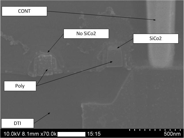
And now individually, polysilicon to the right of DTI with silicide:

And polysilicon over DTI without silicide:
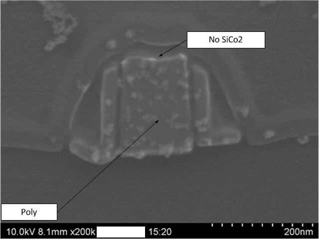
Now we have found the problem, at least it fits into the crystal failure model. Due to the lack of silicide over polysilicon, an increase in the resistance of the bonds between adjacent transistors to hundreds of ohms or even megohms begins to work very slowly and unpredictably. And although we found the problem, it is necessary to find a solution to this problem. To do this, an analysis was made of another part of the scheme where the polysilicon width over DTI is more than 180 nm (minimally resolved and for which we found a problem). Such an area was found; the polysilicon width at this location is 500 nm. At the same time, we determine how the CONT jumpers to polysilicon behave if they are located above the DTI.
When cutting FIB, two perpendicular slices were specially prepared, allowing a complete picture of the state of silicide over polysilicon over DTI.
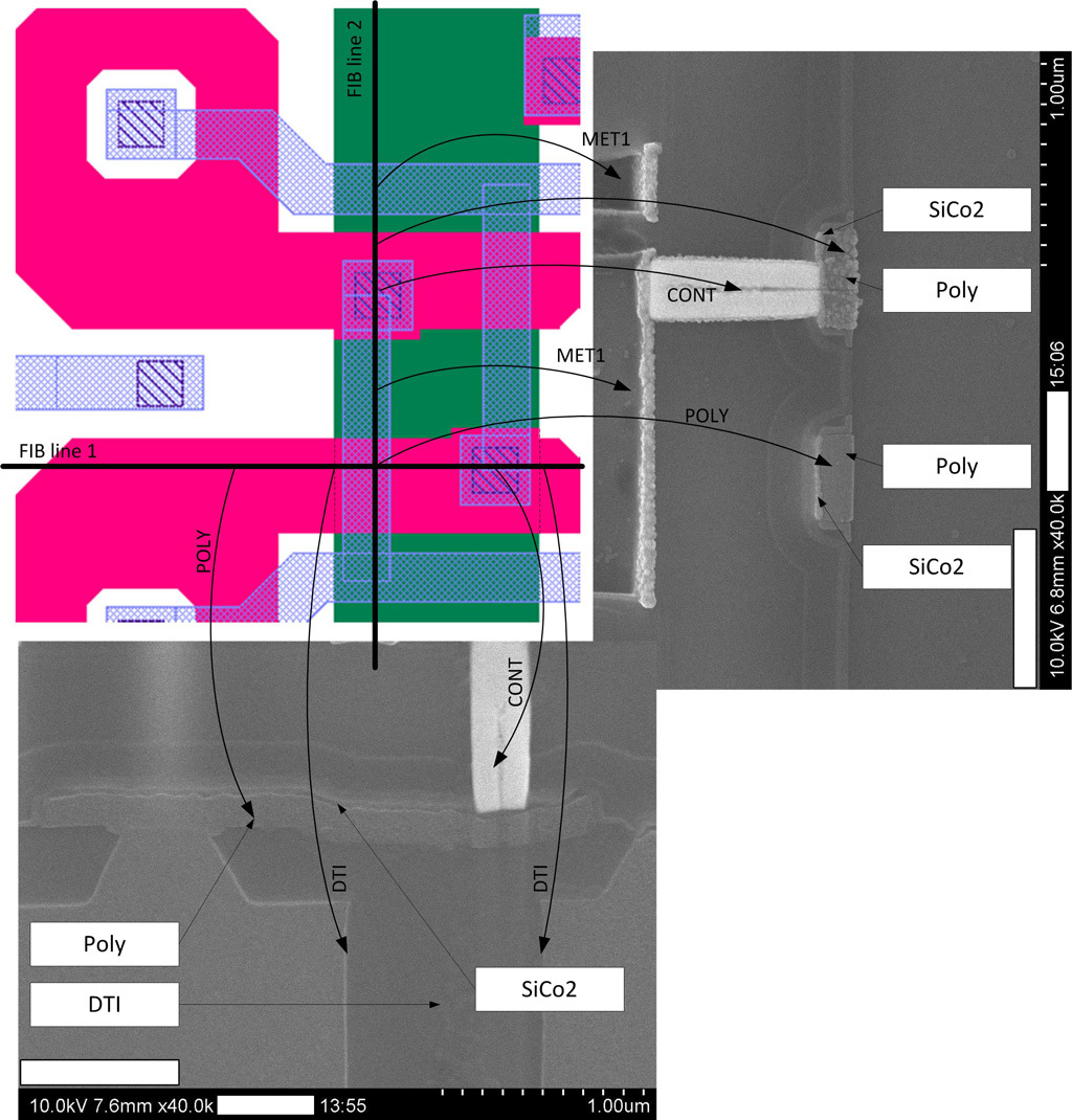
The photo shows that CONT is connected to POLY without any problems. A silicide formed over polysilicon in full. On the horizontal cut of FIB Line 1, the silicide did not turn white due to the fact that its longitudinal depth (for the electron flux of the microscope) is ~ 250 nm and has a weak reflection, in contrast to the vertical cut of FIB Line2, the silicide depth there is up to 2000 nm and he turned white. But on a horizontal cut, a layer of silicide is still clearly visible. We, as crystal developers, do not undertake to judge why a silicide does not form over polysilicon over DTI if its width is 180 nm. The crystal manufacturer has also come to a similar conclusion, and as a solution to the problem, it has forbidden to drive polysilicon conductors with a width of less than 1 μm over the DTI.
The microcircuit is made according to the technology of 180 nm. With special features that allow digital logic with a high density and a typical 1.8V power supply and an analog component with operating voltages up to 200V to be placed on a single chip. And in conjunction with operating temperatures up to 150-170С makes this technology very popular in industrial and automotive electronics.
To begin with, we carried out layer-by-layer etching of crystals with stopping and full photographing at each technological level. The level of the sixth metal is MET6 (some elements of the photographs are hidden).
Fifth metal level MET5:
Jumper level between the fifth and fourth metals VIA4:
Well and so on, in total we got about 5 GB of photos.
Unfortunately, even very accurate layer-by-layer etching causes various destruction of crystal structures. And to determine that this is a technological marriage of production or the result of the preparation is very difficult. Usually, the criterion is repeatability, if the effects are similar on several samples, then these are technological problems, if the effects are unique for each test sample, then this is the result of the preparation. For example, defects were found in the area of the nutrition rings. At the level of the sixth metal they are not visible, but starting from the fifth metal they began to appear:
At the level of jumpers between the fifth and fourth metals they became even more
visible : At the level of the third metal they are already clearly visible:
But the defects are unique for each sample and so far are attributed to the problems of the etching process
Missing or incompletely formed vias were found at the bridges between polysilicon and the first metal, unfortunately the resolution of the optical microscope is already at the limit and they are visible as dark spots:
These defects with large correlations were repeated on several samples:
There were a lot of such defects on the crystal flying out "vias, mainly they were in the area of the digital core and memory blocks. In the following figure, they are marked with red dots, red rectangles indicate areas damaged during etching:
As noted earlier, optical microscopy does not allow us to visually assess the condition, and we had to use an electron microscope, and where the electron microscope is, it’s not far from the FIB (Focused Ions Beam) installation. FIB allows a directional ion beam to cut crystal elements with nanometer accuracy or, on the contrary, apply new layers to it, for example, connect adjacent conductors.
We performed a crystal cut in the region where the intensity of the “flying out” VIA was maximum:
And it seems that they found a problem, indeed there was no corresponding VIA on the slice (in this technical process they are designated as CONT). But technologists and topologists of the circuit expressed doubt that we were in the right place. So the remarks of the technologists boiled down to the fact that there should have been at least something, and there was a clean insulator. And topologists pointed out that although the slice is very similar to the topology, it differs from it. In particular, in the topology drawing, the transitional VIA1 and CONT are not coaxial, but on the cut they are located strictly one above the other, and this cannot be attributed to technological spread.
In a more detailed analysis, it was found that this region is really in the same region, but with an indent of about 2 μm, which is completely suitable for this section and it really does not have this transition between the first metal and polysilicon. We just got there.
With the repeated cut, we were able to get to the required area, and there were no more complaints about the transition windows:
As you can see, now the whole photograph of the slice completely repeats the topology and the VIA between the different layers are spaced. All vias are fully formed. And the reason for the inoperability of the crystals was not found.
When viewing through the electron microscope the level of polysilicon (indicated by POLY), it was noted that in the field of separation of P-channel and N-channel transistors using a deep dielectric (indicated in the DTI figures), polysilicon has some thickening.
For clarity, a topology drawing is applied to the photo. But at the same time, any gaps or shorts between the various polysilicon tires are not visible. But in any case, we decided to see what is happening there with polysilicon.
But first, let's understand what polysilicon (POLY) is and why it is needed. Polysilicon compounds are a trace resource of the lowest crystal level. The main compounds in the crystal are provided through the metals of the upper layers. But neighboring transistors of one valve can be connected using polysilicon. In order for polysilicon to become electrically conductive it is alloyed (by adding impurities of fluorine, boron or arsenic), sometimes all polysilicon in the crystal is doped, sometimes not. In the case when polysilicon is not doped, its conductivity is achieved by applying a layer of silicide over it (this is a compound of silicon with metals). So in our case, the conductivity of polysilicon over the deep dielectric region (DTI) is achieved by applying a layer of silicide (SiCo2) on it .
For this, we made another cut, which allows us to see the structure of polysilicon over deep and shallow dielectrics.
Already in this photo you can see that above the polysilicon, which is located to the right of the DTI, a white "cap" of silicide is visible, and above polysilicon directly above DTI it is not.
Zoom in:
Zoom in:
And now individually, polysilicon to the right of DTI with silicide:
And polysilicon over DTI without silicide:
Now we have found the problem, at least it fits into the crystal failure model. Due to the lack of silicide over polysilicon, an increase in the resistance of the bonds between adjacent transistors to hundreds of ohms or even megohms begins to work very slowly and unpredictably. And although we found the problem, it is necessary to find a solution to this problem. To do this, an analysis was made of another part of the scheme where the polysilicon width over DTI is more than 180 nm (minimally resolved and for which we found a problem). Such an area was found; the polysilicon width at this location is 500 nm. At the same time, we determine how the CONT jumpers to polysilicon behave if they are located above the DTI.
When cutting FIB, two perpendicular slices were specially prepared, allowing a complete picture of the state of silicide over polysilicon over DTI.
The photo shows that CONT is connected to POLY without any problems. A silicide formed over polysilicon in full. On the horizontal cut of FIB Line 1, the silicide did not turn white due to the fact that its longitudinal depth (for the electron flux of the microscope) is ~ 250 nm and has a weak reflection, in contrast to the vertical cut of FIB Line2, the silicide depth there is up to 2000 nm and he turned white. But on a horizontal cut, a layer of silicide is still clearly visible. We, as crystal developers, do not undertake to judge why a silicide does not form over polysilicon over DTI if its width is 180 nm. The crystal manufacturer has also come to a similar conclusion, and as a solution to the problem, it has forbidden to drive polysilicon conductors with a width of less than 1 μm over the DTI.