One for all
It somehow happened that in several recent projects I used various modifications of IFA (Inverted А Antenna) as a radiating element . This workhorse is actively used in a huge number of modern wireless devices. I would like to devote this post to the species diversity of IFA.
Try to enter the magic phrase Inverted F Antenna (IFA) in a search engine and you will see an incredible variety of versions of this antenna - from wired giants to planar ceramic midgets. What is the reason for such popularity?
With the development of mobile communications, laptop computers, navigation terminals, wearable electronics, etc. there was a need for a compact and functional antenna, which could be located on the printed circuit board, occupying (only one layer) / (minimum space), as well as being insensitive to what is located in other layers and on the back of the board. One of these decisions was the IFA. The popularity of this solution is explained by the fact that the IFA has a relatively wide band of operating frequencies (up to 10% of the center frequency), relatively high efficiency (ratio of radiated power to input), reaching 65%, multi-band support, small dimensions, and the ability to work with vertical and horizontal polarized ... The list of advantages is quite impressive. You also need to add that the popularity of IFA is also due to the fact that it has been studied and described in sufficient detail (in terms of the dependence of its characteristics on geometry). If you are interested in technical details, send to the article V.I. Slusara“PIFA Antennas for Mobile Communications: A Variety of Designs”
However, for many developers, it’s interesting to have an antenna made on a printed circuit board in a single technological cycle with the topology of the developed device. And here I would like to give a few examples.
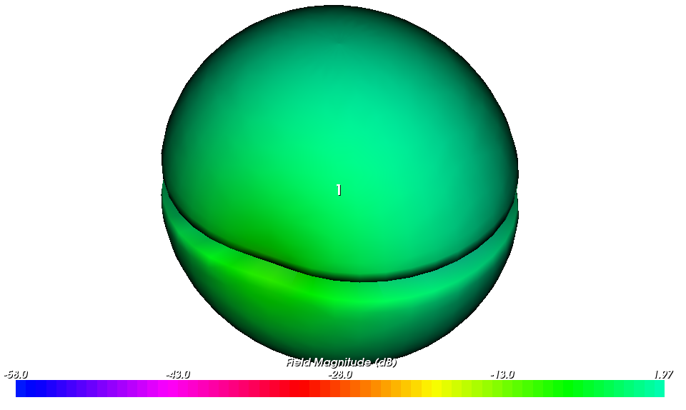
When there is a lot of space on the printed circuit board (PCB), you can make a “classic” PIFA (Printed IFA). As, for example, in the images below
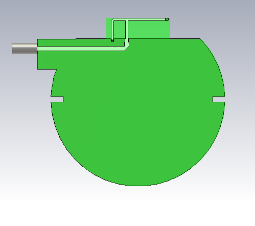
Appearance of a printed circuit board with an antenna Directivity

diagram
True, most often you have to find ways to reduce the space occupied by the antenna. One of such methods - “ZigZag” PIFA - is described in a document known to many (I think so) . I will illustrate ...

Topology of the board with ZigZag ”PIFA
The radiation pattern for such a structure
And lastly I would like to show a variant of dual-band PIFA (for example, for Wi-Fi networks), a little “minimized” to reduce the occupied space.
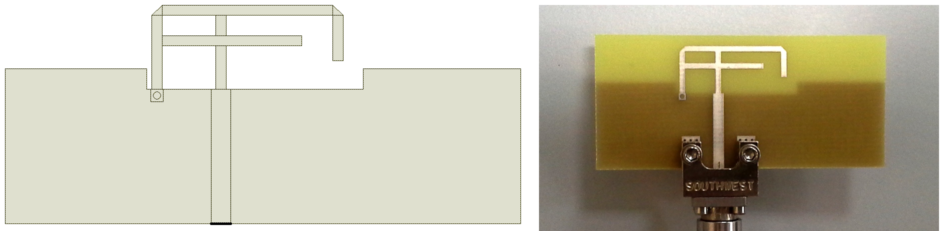
The calculated topology and PIFA breadboard for the 2.4 GHz and 5.2 GHz bands.

The radiation pattern for the 2.45 GHz frequency
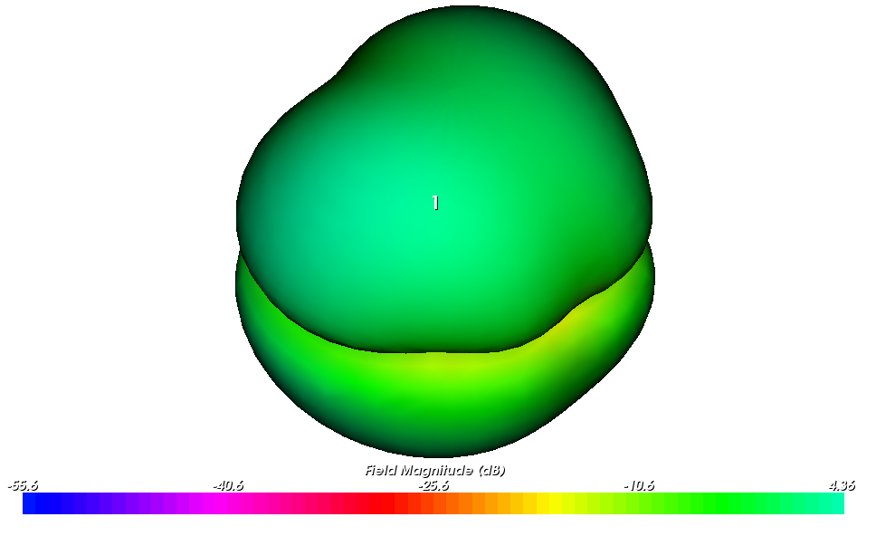
pattern. The radiation pattern for the 5.25 GHz frequency.
And this is only a small part of the IFA species diversity ...
PS I was pleasantly surprised when I managed to find several interesting articles in Russian on the subject I declared on the site of V.I. Slyusara , and also was able to draw something from the book of I.V. Goncharenko “HF and VHF antennas part 6: VHF antennas” .
Try to enter the magic phrase Inverted F Antenna (IFA) in a search engine and you will see an incredible variety of versions of this antenna - from wired giants to planar ceramic midgets. What is the reason for such popularity?
With the development of mobile communications, laptop computers, navigation terminals, wearable electronics, etc. there was a need for a compact and functional antenna, which could be located on the printed circuit board, occupying (only one layer) / (minimum space), as well as being insensitive to what is located in other layers and on the back of the board. One of these decisions was the IFA. The popularity of this solution is explained by the fact that the IFA has a relatively wide band of operating frequencies (up to 10% of the center frequency), relatively high efficiency (ratio of radiated power to input), reaching 65%, multi-band support, small dimensions, and the ability to work with vertical and horizontal polarized ... The list of advantages is quite impressive. You also need to add that the popularity of IFA is also due to the fact that it has been studied and described in sufficient detail (in terms of the dependence of its characteristics on geometry). If you are interested in technical details, send to the article V.I. Slusara“PIFA Antennas for Mobile Communications: A Variety of Designs”
However, for many developers, it’s interesting to have an antenna made on a printed circuit board in a single technological cycle with the topology of the developed device. And here I would like to give a few examples.
When there is a lot of space on the printed circuit board (PCB), you can make a “classic” PIFA (Printed IFA). As, for example, in the images below
Appearance of a printed circuit board with an antenna Directivity
diagram
True, most often you have to find ways to reduce the space occupied by the antenna. One of such methods - “ZigZag” PIFA - is described in a document known to many (I think so) . I will illustrate ...
Topology of the board with ZigZag ”PIFA
The radiation pattern for such a structure
And lastly I would like to show a variant of dual-band PIFA (for example, for Wi-Fi networks), a little “minimized” to reduce the occupied space.
The calculated topology and PIFA breadboard for the 2.4 GHz and 5.2 GHz bands.
The radiation pattern for the 2.45 GHz frequency
pattern. The radiation pattern for the 5.25 GHz frequency.
And this is only a small part of the IFA species diversity ...
PS I was pleasantly surprised when I managed to find several interesting articles in Russian on the subject I declared on the site of V.I. Slyusara , and also was able to draw something from the book of I.V. Goncharenko “HF and VHF antennas part 6: VHF antennas” .