Digital X-ray: from alpha to gamma
Hi Habr!
It has long been itching to write something good and eternal about digital X-ray, which I have been doing for 5 years already. About myself - 12 years in the development of iron. He started as a constructor, then there was circuit design, development of printed circuit boards, documentation development, work with CNC, HW / SW integration, project management, marketing. In general - with the world on a string.
We develop and manufacture digital flat panel X-ray detectors for industry and medicine in the Russian Federation. If anyone has forgotten what x-ray is, we look at the “Experience of fluoroscopy at home” , “ Home- made X-ray computed tomography scanner” , but do not forget about the harm of ionizing radiation during home experiments.
First of all for medical professionals, this is the largest market. Film X-ray is outliving its age, in large cities everywhere there is a figure.
In the second - the security forces. In scanners, a narrow-line detector is used, but when it is necessary to obtain high image quality, for example, when it is banned in unexpected places on the human body or when searching for bookmarks / bugs in equipment, a flat panel detector is used.
In the third - to production workers. This is a quality control of welding, castings, soldering of metals and installation of electronic components. If welding and castings still fit tightly on the analogue, since the standard for using digital X-rays was released in the Russian Federation only in 2017, serious operators of circuit installation lines have X-ray control for themselves at least BGA chips.
The first X-ray recorder was a film, it is produced in the form of cassettes of different sizes and sensitivity, the principle of operation is the reaction of a photosensitive substance to X-rays and the subsequent development / amplification. It is difficult, for a long time, I made a mistake in the process of exposure - you will know about it after the development.
Naturally natural laziness pushed for a search for a more convenient way and they became computerized radiography (CR). At the entrance we have a storage phosphor plate, it retains the hidden X-ray image. To see the result, the plate is placed in a digitizer, where the IR laser scans the entire surface, and the photosensor captures the luminescence. So get a digital image and then overwrite the previous flare. The diameter of the laser beam (25-100 microns) determines the resolution of the system. Easier than analog, but not instantly. The plate is enough for several thousand exposures.
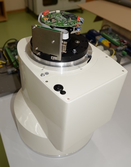
Further, progress gave rise to various systems of instant transformation, for example, an X-ray image intensifier (XRI). URI allowed to work in real time, albeit with distortion. The principle of operation - at the entrance there is a phosphor (scintillator), which generates visible light, which produces electrons on the photocathode, which are accelerated and recorded again by the phosphor, then there is a lens and a CCD sensor. Not easy, yes? One of the advantages of such a system was the possibility of focusing the electron beam and scaling the image; the minuses were the geometric distortions of the X-ray optical converter (REOP) and its size. This good could weigh under 50 kilograms. The URI looks something like this (the CCD camera and the hulk of the REOP are visible):
The next stage is CCD-based detectors. This is modernity, the same scintillator, optics and the sensor itself. Pros - high resolution, from 2kx2k. Cons - CCD sensor size of about 2x2 cm, remember the cameras. Used in microtomography, as a cheap analogue of flat panel detectors.
Almost all modern detectors are built on the basis of CMOS or TFT matrices, we do on CMOS. The size of the matrix from 10x10 cm to 40x40 cm, which is not bad. CMOS matrix is less than TFT, but 25-70 microns pixel. TFT with dimensions of 40x40 cm have a pixel of 130-200 microns. When high sensitivity is needed (mammography, microtomography), CMOS is usually set, in other cases TFT. All sensors are manufactured by Asia.
The detector circuit is shown in the figure. X-rays are converted to optical radiation using a scintillator layer. Since the CMOS sensor does not like ionizing radiation, we separate it from the phosphor by a fiber-optic plate (GPM). GPs are also not simple, but with cerium additives, so as not to darken over time under X-rays.
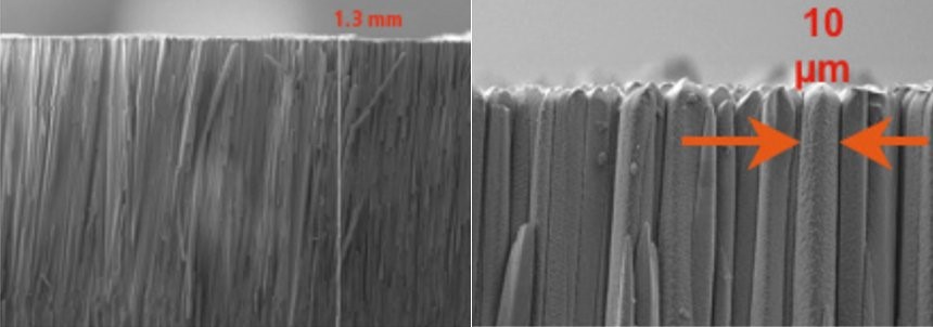
Typically, the scintillator material is cesium iodide (CsI) or gadolinium oxysulfide (GadOx). They differ in structure, CsI is needle-like crystals through which light passes like a fiber, GadOx is a continuous layer, in which scattering effects are strong. This is what a cesium iodide crystal looks like:
X-ray conversion into light and the passage of phosphor through a layer is quite a complicated process, everything plays: thickness, type of deposition (crystals should be grown directly on the SPM), radiation energy. I will not dwell on this in detail, who wants to learn more about sensitivity - read “X-Ray Detector Characterization - a comparison of scintillators”. Roughly - up to 60 kV energy, GadOx is used, above 100 - CsI, in the middle both options are. For reference: mammography is the range from 20 to 40 kV, conventional medicine from 50 to 150 kV, industry from 150 to 450 kV.
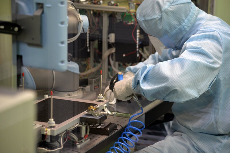
Yes, I completely forgot, it’s just not possible to collect all this stuff into a single block, we need a clean room and equipment to combine the sensors with maximum precision, we can do it in 1 pixel. GigE Vision / Genicam
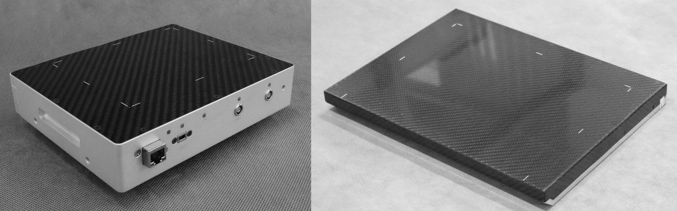
is often used as a data transfer protocol , since Gigabit Ethernet acts as the physical layer. With a large matrix size and dynamic operation mode, it is no longer enough; you have to use Full CameraLink or optical fiber. As a result, the detectors look like this:
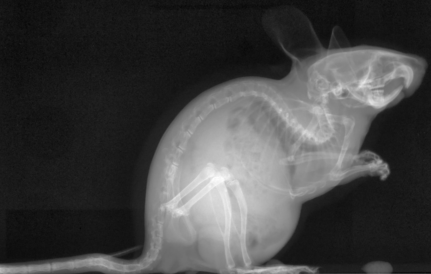
You can shoot welding, ceramics, metal powder printing, boards with BGA chips, laboratory animals and do tomography of small objects. If anyone is interested and has fresh ideas on the application - write, we will be happy.
It has long been itching to write something good and eternal about digital X-ray, which I have been doing for 5 years already. About myself - 12 years in the development of iron. He started as a constructor, then there was circuit design, development of printed circuit boards, documentation development, work with CNC, HW / SW integration, project management, marketing. In general - with the world on a string.
We develop and manufacture digital flat panel X-ray detectors for industry and medicine in the Russian Federation. If anyone has forgotten what x-ray is, we look at the “Experience of fluoroscopy at home” , “ Home- made X-ray computed tomography scanner” , but do not forget about the harm of ionizing radiation during home experiments.
Who does all this need?
First of all for medical professionals, this is the largest market. Film X-ray is outliving its age, in large cities everywhere there is a figure.
In the second - the security forces. In scanners, a narrow-line detector is used, but when it is necessary to obtain high image quality, for example, when it is banned in unexpected places on the human body or when searching for bookmarks / bugs in equipment, a flat panel detector is used.
In the third - to production workers. This is a quality control of welding, castings, soldering of metals and installation of electronic components. If welding and castings still fit tightly on the analogue, since the standard for using digital X-rays was released in the Russian Federation only in 2017, serious operators of circuit installation lines have X-ray control for themselves at least BGA chips.
Minute of history
The first X-ray recorder was a film, it is produced in the form of cassettes of different sizes and sensitivity, the principle of operation is the reaction of a photosensitive substance to X-rays and the subsequent development / amplification. It is difficult, for a long time, I made a mistake in the process of exposure - you will know about it after the development.
Naturally natural laziness pushed for a search for a more convenient way and they became computerized radiography (CR). At the entrance we have a storage phosphor plate, it retains the hidden X-ray image. To see the result, the plate is placed in a digitizer, where the IR laser scans the entire surface, and the photosensor captures the luminescence. So get a digital image and then overwrite the previous flare. The diameter of the laser beam (25-100 microns) determines the resolution of the system. Easier than analog, but not instantly. The plate is enough for several thousand exposures.
Further, progress gave rise to various systems of instant transformation, for example, an X-ray image intensifier (XRI). URI allowed to work in real time, albeit with distortion. The principle of operation - at the entrance there is a phosphor (scintillator), which generates visible light, which produces electrons on the photocathode, which are accelerated and recorded again by the phosphor, then there is a lens and a CCD sensor. Not easy, yes? One of the advantages of such a system was the possibility of focusing the electron beam and scaling the image; the minuses were the geometric distortions of the X-ray optical converter (REOP) and its size. This good could weigh under 50 kilograms. The URI looks something like this (the CCD camera and the hulk of the REOP are visible):
The next stage is CCD-based detectors. This is modernity, the same scintillator, optics and the sensor itself. Pros - high resolution, from 2kx2k. Cons - CCD sensor size of about 2x2 cm, remember the cameras. Used in microtomography, as a cheap analogue of flat panel detectors.
Our days
Almost all modern detectors are built on the basis of CMOS or TFT matrices, we do on CMOS. The size of the matrix from 10x10 cm to 40x40 cm, which is not bad. CMOS matrix is less than TFT, but 25-70 microns pixel. TFT with dimensions of 40x40 cm have a pixel of 130-200 microns. When high sensitivity is needed (mammography, microtomography), CMOS is usually set, in other cases TFT. All sensors are manufactured by Asia.
The detector circuit is shown in the figure. X-rays are converted to optical radiation using a scintillator layer. Since the CMOS sensor does not like ionizing radiation, we separate it from the phosphor by a fiber-optic plate (GPM). GPs are also not simple, but with cerium additives, so as not to darken over time under X-rays.
Typically, the scintillator material is cesium iodide (CsI) or gadolinium oxysulfide (GadOx). They differ in structure, CsI is needle-like crystals through which light passes like a fiber, GadOx is a continuous layer, in which scattering effects are strong. This is what a cesium iodide crystal looks like:
X-ray conversion into light and the passage of phosphor through a layer is quite a complicated process, everything plays: thickness, type of deposition (crystals should be grown directly on the SPM), radiation energy. I will not dwell on this in detail, who wants to learn more about sensitivity - read “X-Ray Detector Characterization - a comparison of scintillators”. Roughly - up to 60 kV energy, GadOx is used, above 100 - CsI, in the middle both options are. For reference: mammography is the range from 20 to 40 kV, conventional medicine from 50 to 150 kV, industry from 150 to 450 kV.
Yes, I completely forgot, it’s just not possible to collect all this stuff into a single block, we need a clean room and equipment to combine the sensors with maximum precision, we can do it in 1 pixel. GigE Vision / Genicam
is often used as a data transfer protocol , since Gigabit Ethernet acts as the physical layer. With a large matrix size and dynamic operation mode, it is no longer enough; you have to use Full CameraLink or optical fiber. As a result, the detectors look like this:
You can shoot welding, ceramics, metal powder printing, boards with BGA chips, laboratory animals and do tomography of small objects. If anyone is interested and has fresh ideas on the application - write, we will be happy.