Getting Started Learning Cortex-M with the STM32 Example, Part 2
- Tutorial
This article is a continuation of the Cortex-M core microcontroller programming cycle.
The first article can be read here:
We begin to study Cortex-M using the STM32 as an example.
The objective of the articles is to describe in detail the features that arise when programming MK. The material is not intended for those who want to run an example of a blinking LED in 10 minutes. I will try to describe in detail what is often hidden from beginners so as not to scare them.
I really want programmers using standard libraries, templates, examples, etc. understand how it all works. And in the absence of these very libraries and examples, they could independently solve their problem.
The main emphasis is on studying the documentation for the Cortex-M core and the documentation for a specific controller.
This time we will talk about interruptions, as well as some issues of memory architecture and MK firmware structure will be raised.
For reasons that are not entirely clear to me, you cannot go to the ARM website and download the full documentation for the Cortex-M4 core. Yes, and on the Cortex-M3 is also impossible.
Have to read a few documents.
1. Learning will have to start with the Cortex ™ -M3 TechnicalReference Manual Revision: r1p1 - the very first revision of the technical specification for the Cortex-M3 core
2. All further revisions and descriptions of the Cortex ™ -M4 TechnicalReference Manual describe only general data and changes from the previous document.
So please do not be surprised at the links to the specifications of another kernel.
First of all, you need to understand what interrupts are.
Cortex-M MK has two concepts that often confuse Interrupt and Event .
Event is an event (hardware or software) that the core or peripheral units can respond to. One of the reaction options may be interruption.
Interrupt is the interruption of the program and the transfer of control to a specialized section of the interrupt handler.
The relationship between Event and Interrupt is as follows:
Each Interrupt is called by Event, but not every Event is called Interrupt.
In addition to interrupts, events can activate other MK features.
Interrupt management and handling is performed by the NIC Vested Vectored Interrupt Controller (VIC) . The interrupt controller is part of the Cortex-M core. The documentation for this controller should begin to be studied with the Cortex ™ -M3 TechnicalReference Manual Revision: r1p1
When an event occurs, the interrupt controller automatically interrupts the execution of the main program and calls the corresponding interrupt function. After exiting the function of the interrupt handler, the program continues execution from the place where the interrupt occurred. Everything happens automatically (with the correct configuration of NVIC, but more on that below).
The name itself shows that the NVIC controller supports interrupt nesting and priorities. Each interrupt is assigned a priority when configuring NVIC. If a high-priority interrupt occurs during the processing of a low-priority interrupt, then it, in turn, will interrupt the low-priority interrupt handler.
This post does not claim to be complete, I recommend that you study the interrupt section in the Cortex ™ -M3 Technical Reference Manual . Since this part of the kernel has not changed, its description is given in the first revision of r1p1 to the Cortex-M3 core.
When an interrupt is triggered, NVIC switches the kernel to interrupt processing mode. After switching to the interrupt processing mode, the kernel registers are pushed onto the stack. Directly during the writing of the register values to the stack, the initial address of the interrupt processing function is sampled.
The program status register ( Program Status Register (PSR) ), program counter ( Program Counter (PC) ) and communication register ( Link Register (LR) ) are moved onto the stack . Kernel register descriptions are provided in the Cortex-M4 Generic User Guide . Due to this, the state in which the kernel was before entering the interrupt processing mode was remembered.
Registers R0 through R3 and R12 are also saved. These registers are used in the instructions for passing parameters, therefore, placing them on the stack makes it possible to use them in the interrupt function, and R12 often acts as the working register of the program.
Upon completion of the interrupt processing, all actions will be performed in the reverse order: the contents of the stack are extracted and, in parallel with this, the return address is sampled.
From the moment the interrupt is initiated until the first handler instruction is executed, the interrupt takes 12 clock cycles, the same time is needed to resume the main program after the interrupt is completed.
As mentioned above, NVIC supports interrupts with different priorities that can interrupt each other. In this case, various situations may arise, the processing of which is optimized differently.
1. Suspend a low priority interrupt
In this situation, the processing of the low priority interrupt is terminated. The next 12 cycles, the new data set is saved onto the stack and processing of the high-priority interrupt starts. After its processing, the contents of the stack are automatically extracted and processing of the low-priority interrupt is resumed.
There are no big differences from the interruption of the main program.
2. Continuous interrupt handling
This situation can occur in two cases: if two interrupts have the same priority and occur simultaneously, if a low-priority interrupt occurs during processing of a high-priority.
In this case, intermediate operations on the stack are not performed. Only the address handler of the low-priority interrupt is loaded and the transition to its execution occurs. Avoiding stack operations saves 6 clock cycles. The transition to the next interrupt occurs not in 12 clock cycles, but in only 6.
3. The delay of a high-priority interrupt
The situation arises if a high-priority interrupt occurs in the transition to processing low-priority (for those same 12 clock cycles). In this case, the transition to a high-priority interrupt will occur at least 6 cycles from the moment it occurs (the time required to load the address of the interrupt handler and go to it). Return to low priority is already described above.
In addition to simply setting the priority of interrupts, NVIC implements the ability to group priorities.
Interrupts in a group with a higher priority can interrupt the interrupt handlers of a group with a lower priority. interrupts from the same group, but with different priorities within the group, cannot interrupt each other. The priority within the group determines only the order in which the handler is called when both events have been activated.
The interrupt priority value is set in the Interrupt Priority Registers (see Cortex-M4 Generic User Guide ). At the same time, part of the bits is responsible for the priority of the group in which the interrupt is located, and part for priority within the group.
Setting the bit allocation to group priority or priority within a group is done using the Application Interrupt and Reset Control Register (ATTENTION !!! see the Cortex-M4 Generic User Guide ).
As you probably noticed, the Cortex-M4 Generic User Guide says that setting priorities and grouping priorities depends on a particular implementation defined implementation .
But further not a very pleasant thing. In the Reference manual to the STM32F407 MK, there is almost no information about NVIC. But there is a link to a separate document. In order to deal with the implementation of NVIC in STM32, you will have to read another document - STM32F3xxx and STM32F4xxx Cortex-M4 programming manual. Generally speaking, I advise you to carefully study this document on all other issues, the kernel work is described in more detail in it than in the documentation from ARM.
In it, you can already find:
Of the possible 8 priority bits, only 4 are used. But this is quite enough for most tasks.
Suppose that we have the task of launching a launch vehicle by pressing the red button, but only if the key is turned.
It makes absolutely no sense to generate an interrupt to turn the key. But the interruption by pressing the red digging we need. In order to enable / disable various interrupt vectors, there is masking of interrupts.
Interrupt masking is done using the Interrupt Set-enable Registers .
If the interrupt is masked, this does not mean that the peripherals are not generating events! It’s just that NVIC does not call a handler for this event.
All possible interrupts supported by NVIC are written to the interrupt vector table. At its core, an interrupt vector table is nothing more than a list of function addresses for interrupt handlers. The number in the list corresponds to the interrupt number.
As written in the Cortex-M4 Generic User Guide , NVIC supports up to 240 different interrupt vectors. But the implementation already depends on the specific manufacturer.
In the kernel description, only kernel exception interrupts are standardized (see section 2.3.2 Exception types in the Cortex-M4 Generic User Guide ):
I suggest you familiarize yourself with the description of these exceptions. Some of these will be addressed in future articles.
The remaining interruptions are unique to MK. You can find the description of the vector table of your MK in the corresponding Reference manual (see Vector table for STM32F405xx / 07xx and STM32F415xx / 17xx). STM32F4xx controllers support 81 interrupt vectors. You may notice that in this table all peripheral blocks are listed (and some more than once).
Almost all peripheral units generate interrupts so that the kernel is distracted to work with it only upon the occurrence of a significant event (for example, receiving data via UART).
Having understood the principles of interrupt operation in Cortex-M, it remains only to understand where the interrupt table is stored.
For this, it is worth considering the boot process and the controller firmware structure. This time we will only consider loading from the built-in flash memory.
The vector table at the beginning of the flash memory address space should be at least (see the Cortex-M3 Technical Reference Manual :
From the beginning of flash memory, the kernel reads the value of SP (stack top addres) and PC (reset routine location). Thus, the function starts automatically, with the address read in the PC register. It could be, for example, main.
After the required four components, there may be a further table of interrupt vectors. The main thing is to keep order.
If you wish, you can place the table of interrupt vectors in another memory area, but then, you need to tell NVIC where we moved the table. The Vector Table Offset Register is responsible for this displacement of the vector table (see the Cortex-M4 Technical Reference Manual . This may be necessary to write the built-in bootloader for new software (bootloader), but about this some other time.
An example is created for the STM32F4Discovery debug board .
When the button is pressed, LED3 should light up. When contacts PC6 and GND are closed, LED5 lights up.
In the programming process, let's play with the interrupt priorities and see what this will lead to.
We will find the button and the LED in the documentation for the board :

When the button is not pressed, the pin PA0 will be a logical zero, when the button is pressed, the button will display logical 1 (3.3V).
LED3 is connected to pin PD13.
LED5 is connected to pin PD14.
The most interesting thing with the PC6 pin is that it is directly connected to the pin connector. We will need to ensure that logical 1 is logged when it is not shorted to the GND pin. How to do this will be discussed below.
For our task, it is necessary to configure pins PD13 and PD14 as a weekend. You can read about how to do this in a previous article .
Setting up the PA0 pin is also quite simple - you need to configure it for input. Despite the fact that after counting the MK almost all the pins are configured for input, it is highly advisable to explicitly register this initialization.
With the PC7 pin, everything is somewhat more interesting. Since he is "hanging in the air", his condition is not defined. We need to ensure that his condition is always “1”. To do this, activate the pull-up in the GPIO block. In our case, you need a pull-up to power - PULL UP.
The pull-up is activated using the GPIO port pull-up / pull-down register .
To perform our “TK” using interrupts, we need to configure interrupts that will be triggered when the contact PA0 changes from state “0” to state “1”, and the interrupt occurs when contact PC6 changes from state “1” to state “0”.
In the STM32F4xx MK, an EXTI (External interrupt / event controller) controller is used for this purpose . I highly recommend that you familiarize yourself with its functionality in the Reference manual . We need to do as described:
We will need 0 and 6 EXTI lines. To mask the corresponding interrupt lines, write 0x9 to the EXTI_IMR register.
For line PA0, it is necessary to generate an interrupt event on the transition from state “0” to state “1” - on an increasing edge. That is, it is necessary to write 1 to the zero bit of the EXTI_RTSR register.
For PC6 line, on the contrary, it is necessary to generate an interrupt event on the transition from state “1” to state “0” - on the falling edge. That is, it is necessary to write 1 in the sixth bit of the EXTI_FTSR register.
This completes the configuration of the EXTI block. The last item will be implemented when tincture NVIC.
In addition to this, it is necessary to determine which pin from which port is connected to a specific EXTI line. This is done using registers.SYSCFG external interrupt configuration register ( Reference manual ). These registers are located in the System configuration controller , which seems to me not very logical (why not include this setting in EXTI?), But let's leave this fact to ST's conscience.
The processing of a certain interrupt vector is activated using the Interrupt set-enable registers (NVIC_ISERx) registers . Register descriptions are provided in the Cortex-M4 Generic User Guide . The table of interrupt vectors for our MK is given in the Reference manual (see Table 61).
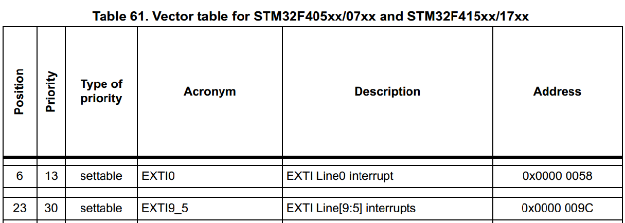
From the table you can see that for line 0 there is a separate interrupt, but lines 5 through 9 generate one interrupt for all.
In addition, from the table we learned the numbers of the vectors we need interrupts. Now you need to write “1” in 6 bits (activation of line interrupt 0 EXTI) register NVIC_ISER0 (address 0xE000E100) and 23 bits of the same register (activation of line interrupt 5-9).
In order to indulge in the interrupt priorities, we will configure priority groups so that 2 bits are responsible for the priority within the group, and 2 bits are responsible for the priority of the group itself. To do this, write the value 0x05FA0500 to the Application interrupt and reset control register ( STM32F3xxx and STM32F4xxx Cortex-M4 programming manual ).
Priority setting is done using the Interrupt Priority Registers registers ( STM32F3xxx and STM32F4xxx Cortex-M4 programming manual ). We will be interested in the Interrupt Priority Register 2 (0xE000E4008) and the Interrupt Priority Register 5 (0xE000E401C) registers.
We will not change priorities yet. Let it be the same for both interrupts.
Functions interrupt handlers are nothing more than just functions of the C language, which neither receive nor return anything (and rightly so - not from anyone and not to whom).
The main rule is that interrupt handling should be done as quickly as possible !!! Otherwise, low priority interrupts can wait too long.
After termination of the interrupt processing it is necessary to reset the activity of the event that caused the interrupt - “clear the interrupt”. The EXTI interrupt is cleared using the EXTI_PR register. Note: record “1” clears the interrupt, record “0” has no effect whatsoever.
If everything is quite simple with the processing of line interrupt 0 EXTI, then with the group of lines 5-9 the question arises - how to determine which line caused the interrupt. You can find this out by checking the register bit of the Pending register (EXTI_PR) - Reference manual .
In order for the vector table with the correct addresses of the interrupt handler functions to be located at the beginning of the MK flash memory, create and connect the startup.c file to the project.

The section itself is set at the beginning of the ROM memory. Addresses can be found here (a document that describes the addressing of STM32 flash memory):

Combination of IAR directive and IAR special functions:
The table itself is filled with addresses of functions that implements an eternal cycle. An exception is made only for the functions of interest to us:
The function called at startup simply jumps to

First, write and redefine all the addresses and bit fields that we need.
First of all, it is worth setting up the grouping of interrupt priorities:
Let me remind you that before you start working with peripheral units, you need to enable their timing:
You cannot work immediately with SYSCFG, you need to wait a few measures. But we will not. Let's get started with initializing the GPIO.
LEDs are initialized in the same way as last time:
The PA0 button and PC7 pin are initialized as input:
That's just for contact PC6 you need to turn on the power pull. Suspending activation is performed using the GPIOC_PUPDR register:
And so, you need to configure the following parameters - enable interrupts for lines 0 and 6, for line 0 interrupt on a rising edge, for line 6 - interrupt on a falling edge:
It remains to configure the pins of which ports are connected to the EXTI line (a strange solution, for example, stellaris MKs can generate an interrupt for any combination of pins, for STM32 this is more difficult):
It remains to configure the interrupt priorities and mask them to initiate processing. Note that the NVIC_IPR registers are available for byte access, which greatly simplifies access only to the necessary priority bytes of individual interrupt vectors. It is enough to make a shift by the value of the number of the interrupt vector (see the listing of definitions). Once again, we recall that EXTI Line 0 has number 6 in the vector table, and EXTI line 5_9 has number 23. For STM32, only the highest 4 bits of priority are of importance:
To demonstrate, the priorities are set different.
Now you can enable interrupts:
From now on, pressing the button and shorting PC6 and GND will cause the call of the interrupt handler functions EXTI_Line0_IntHandler and EXTI_Line6_IntHandler, respectively.
In the interrupt handling functions, it is first necessary to clear the interrupt, after which you can light up the LEDs. To demonstrate interrupt priorities, an eternal loop has been added to one of the handlers. If the priority of an interrupt with an eternal loop is lower than the priority of the second, then it cannot be called. Otherwise, it will be able to interrupt the first. I suggest you try the different values of the interrupt priorities yourself and visually see what this leads to ( ATTENTION - do not forget about the interrupt groups! ).
Just in case, I will give a complete listing of the resulting program.
To check the effect of interrupt priorities and interrupt group priorities, try changing the priorities and observe what happens (two bits - priority within the group, 2 bits - priority of the group).
The first article can be read here:
We begin to study Cortex-M using the STM32 as an example.
The objective of the articles is to describe in detail the features that arise when programming MK. The material is not intended for those who want to run an example of a blinking LED in 10 minutes. I will try to describe in detail what is often hidden from beginners so as not to scare them.
I really want programmers using standard libraries, templates, examples, etc. understand how it all works. And in the absence of these very libraries and examples, they could independently solve their problem.
The main emphasis is on studying the documentation for the Cortex-M core and the documentation for a specific controller.
This time we will talk about interruptions, as well as some issues of memory architecture and MK firmware structure will be raised.
A few words about ARM documentation
For reasons that are not entirely clear to me, you cannot go to the ARM website and download the full documentation for the Cortex-M4 core. Yes, and on the Cortex-M3 is also impossible.
Have to read a few documents.
1. Learning will have to start with the Cortex ™ -M3 TechnicalReference Manual Revision: r1p1 - the very first revision of the technical specification for the Cortex-M3 core
2. All further revisions and descriptions of the Cortex ™ -M4 TechnicalReference Manual describe only general data and changes from the previous document.
So please do not be surprised at the links to the specifications of another kernel.
Interrupt and events
First of all, you need to understand what interrupts are.
Cortex-M MK has two concepts that often confuse Interrupt and Event .
Event is an event (hardware or software) that the core or peripheral units can respond to. One of the reaction options may be interruption.
Interrupt is the interruption of the program and the transfer of control to a specialized section of the interrupt handler.
The relationship between Event and Interrupt is as follows:
Each Interrupt is called by Event, but not every Event is called Interrupt.
In addition to interrupts, events can activate other MK features.
NVIC
Interrupt management and handling is performed by the NIC Vested Vectored Interrupt Controller (VIC) . The interrupt controller is part of the Cortex-M core. The documentation for this controller should begin to be studied with the Cortex ™ -M3 TechnicalReference Manual Revision: r1p1
When an event occurs, the interrupt controller automatically interrupts the execution of the main program and calls the corresponding interrupt function. After exiting the function of the interrupt handler, the program continues execution from the place where the interrupt occurred. Everything happens automatically (with the correct configuration of NVIC, but more on that below).
The name itself shows that the NVIC controller supports interrupt nesting and priorities. Each interrupt is assigned a priority when configuring NVIC. If a high-priority interrupt occurs during the processing of a low-priority interrupt, then it, in turn, will interrupt the low-priority interrupt handler.
How it works?
This post does not claim to be complete, I recommend that you study the interrupt section in the Cortex ™ -M3 Technical Reference Manual . Since this part of the kernel has not changed, its description is given in the first revision of r1p1 to the Cortex-M3 core.
Entering and exiting an interrupt
When an interrupt is triggered, NVIC switches the kernel to interrupt processing mode. After switching to the interrupt processing mode, the kernel registers are pushed onto the stack. Directly during the writing of the register values to the stack, the initial address of the interrupt processing function is sampled.
The program status register ( Program Status Register (PSR) ), program counter ( Program Counter (PC) ) and communication register ( Link Register (LR) ) are moved onto the stack . Kernel register descriptions are provided in the Cortex-M4 Generic User Guide . Due to this, the state in which the kernel was before entering the interrupt processing mode was remembered.
Registers R0 through R3 and R12 are also saved. These registers are used in the instructions for passing parameters, therefore, placing them on the stack makes it possible to use them in the interrupt function, and R12 often acts as the working register of the program.
Upon completion of the interrupt processing, all actions will be performed in the reverse order: the contents of the stack are extracted and, in parallel with this, the return address is sampled.
From the moment the interrupt is initiated until the first handler instruction is executed, the interrupt takes 12 clock cycles, the same time is needed to resume the main program after the interrupt is completed.
Interrupt Nesting
As mentioned above, NVIC supports interrupts with different priorities that can interrupt each other. In this case, various situations may arise, the processing of which is optimized differently.
1. Suspend a low priority interrupt
In this situation, the processing of the low priority interrupt is terminated. The next 12 cycles, the new data set is saved onto the stack and processing of the high-priority interrupt starts. After its processing, the contents of the stack are automatically extracted and processing of the low-priority interrupt is resumed.
There are no big differences from the interruption of the main program.
2. Continuous interrupt handling
This situation can occur in two cases: if two interrupts have the same priority and occur simultaneously, if a low-priority interrupt occurs during processing of a high-priority.
In this case, intermediate operations on the stack are not performed. Only the address handler of the low-priority interrupt is loaded and the transition to its execution occurs. Avoiding stack operations saves 6 clock cycles. The transition to the next interrupt occurs not in 12 clock cycles, but in only 6.
3. The delay of a high-priority interrupt
The situation arises if a high-priority interrupt occurs in the transition to processing low-priority (for those same 12 clock cycles). In this case, the transition to a high-priority interrupt will occur at least 6 cycles from the moment it occurs (the time required to load the address of the interrupt handler and go to it). Return to low priority is already described above.
Interrupt Priorities
In addition to simply setting the priority of interrupts, NVIC implements the ability to group priorities.
Interrupts in a group with a higher priority can interrupt the interrupt handlers of a group with a lower priority. interrupts from the same group, but with different priorities within the group, cannot interrupt each other. The priority within the group determines only the order in which the handler is called when both events have been activated.
The interrupt priority value is set in the Interrupt Priority Registers (see Cortex-M4 Generic User Guide ). At the same time, part of the bits is responsible for the priority of the group in which the interrupt is located, and part for priority within the group.
Setting the bit allocation to group priority or priority within a group is done using the Application Interrupt and Reset Control Register (ATTENTION !!! see the Cortex-M4 Generic User Guide ).
As you probably noticed, the Cortex-M4 Generic User Guide says that setting priorities and grouping priorities depends on a particular implementation defined implementation .
But further not a very pleasant thing. In the Reference manual to the STM32F407 MK, there is almost no information about NVIC. But there is a link to a separate document. In order to deal with the implementation of NVIC in STM32, you will have to read another document - STM32F3xxx and STM32F4xxx Cortex-M4 programming manual. Generally speaking, I advise you to carefully study this document on all other issues, the kernel work is described in more detail in it than in the documentation from ARM.
In it, you can already find:
A programmable priority level of 0-15 for each interrupt. A higher level corresponds to a
lower priority, so level 0 is the highest interrupt priority
Of the possible 8 priority bits, only 4 are used. But this is quite enough for most tasks.
Masking interrupts
Suppose that we have the task of launching a launch vehicle by pressing the red button, but only if the key is turned.
It makes absolutely no sense to generate an interrupt to turn the key. But the interruption by pressing the red digging we need. In order to enable / disable various interrupt vectors, there is masking of interrupts.
Interrupt masking is done using the Interrupt Set-enable Registers .
If the interrupt is masked, this does not mean that the peripherals are not generating events! It’s just that NVIC does not call a handler for this event.
Interrupt Vector Table
All possible interrupts supported by NVIC are written to the interrupt vector table. At its core, an interrupt vector table is nothing more than a list of function addresses for interrupt handlers. The number in the list corresponds to the interrupt number.
As written in the Cortex-M4 Generic User Guide , NVIC supports up to 240 different interrupt vectors. But the implementation already depends on the specific manufacturer.
In the kernel description, only kernel exception interrupts are standardized (see section 2.3.2 Exception types in the Cortex-M4 Generic User Guide ):
- Reset
- Nmi
- Hardfault
- Memmanage
- Busfault
- Usagefault
- SVCall
- Pendsw
- Systick
I suggest you familiarize yourself with the description of these exceptions. Some of these will be addressed in future articles.
The remaining interruptions are unique to MK. You can find the description of the vector table of your MK in the corresponding Reference manual (see Vector table for STM32F405xx / 07xx and STM32F415xx / 17xx). STM32F4xx controllers support 81 interrupt vectors. You may notice that in this table all peripheral blocks are listed (and some more than once).
Almost all peripheral units generate interrupts so that the kernel is distracted to work with it only upon the occurrence of a significant event (for example, receiving data via UART).
Arrangement of interrupt vectors and loading MK
Having understood the principles of interrupt operation in Cortex-M, it remains only to understand where the interrupt table is stored.
For this, it is worth considering the boot process and the controller firmware structure. This time we will only consider loading from the built-in flash memory.
The vector table at the beginning of the flash memory address space should be at least (see the Cortex-M3 Technical Reference Manual :
• stack top address
• reset routine location
• NMI ISR location
• Hard Fault ISR location.
From the beginning of flash memory, the kernel reads the value of SP (stack top addres) and PC (reset routine location). Thus, the function starts automatically, with the address read in the PC register. It could be, for example, main.
After the required four components, there may be a further table of interrupt vectors. The main thing is to keep order.
If you wish, you can place the table of interrupt vectors in another memory area, but then, you need to tell NVIC where we moved the table. The Vector Table Offset Register is responsible for this displacement of the vector table (see the Cortex-M4 Technical Reference Manual . This may be necessary to write the built-in bootloader for new software (bootloader), but about this some other time.
From theory to practice
TOR of the second project
An example is created for the STM32F4Discovery debug board .
When the button is pressed, LED3 should light up. When contacts PC6 and GND are closed, LED5 lights up.
In the programming process, let's play with the interrupt priorities and see what this will lead to.
Iron part
We will find the button and the LED in the documentation for the board :
When the button is not pressed, the pin PA0 will be a logical zero, when the button is pressed, the button will display logical 1 (3.3V).
LED3 is connected to pin PD13.
LED5 is connected to pin PD14.
The most interesting thing with the PC6 pin is that it is directly connected to the pin connector. We will need to ensure that logical 1 is logged when it is not shorted to the GND pin. How to do this will be discussed below.
GPIO setup
For our task, it is necessary to configure pins PD13 and PD14 as a weekend. You can read about how to do this in a previous article .
Setting up the PA0 pin is also quite simple - you need to configure it for input. Despite the fact that after counting the MK almost all the pins are configured for input, it is highly advisable to explicitly register this initialization.
With the PC7 pin, everything is somewhat more interesting. Since he is "hanging in the air", his condition is not defined. We need to ensure that his condition is always “1”. To do this, activate the pull-up in the GPIO block. In our case, you need a pull-up to power - PULL UP.
The pull-up is activated using the GPIO port pull-up / pull-down register .
EXTI Interrupts
To perform our “TK” using interrupts, we need to configure interrupts that will be triggered when the contact PA0 changes from state “0” to state “1”, and the interrupt occurs when contact PC6 changes from state “1” to state “0”.
In the STM32F4xx MK, an EXTI (External interrupt / event controller) controller is used for this purpose . I highly recommend that you familiarize yourself with its functionality in the Reference manual . We need to do as described:
Hardware interrupt selection
To configure the 23 lines as interrupt sources, use the following procedure:
• Configure the mask bits of the 23 interrupt lines (EXTI_IMR)
• Configure the Trigger selection bits of the interrupt lines (EXTI_RTSR and EXTI_FTSR)
• Configure the enable and mask bits that control the NVIC IRQ channel mapped to the external interrupt controller (EXTI) so that an interrupt coming from one of the 23 lines can be correctly acknowledged.
We will need 0 and 6 EXTI lines. To mask the corresponding interrupt lines, write 0x9 to the EXTI_IMR register.
For line PA0, it is necessary to generate an interrupt event on the transition from state “0” to state “1” - on an increasing edge. That is, it is necessary to write 1 to the zero bit of the EXTI_RTSR register.
For PC6 line, on the contrary, it is necessary to generate an interrupt event on the transition from state “1” to state “0” - on the falling edge. That is, it is necessary to write 1 in the sixth bit of the EXTI_FTSR register.
This completes the configuration of the EXTI block. The last item will be implemented when tincture NVIC.
In addition to this, it is necessary to determine which pin from which port is connected to a specific EXTI line. This is done using registers.SYSCFG external interrupt configuration register ( Reference manual ). These registers are located in the System configuration controller , which seems to me not very logical (why not include this setting in EXTI?), But let's leave this fact to ST's conscience.
NVIC setup
The processing of a certain interrupt vector is activated using the Interrupt set-enable registers (NVIC_ISERx) registers . Register descriptions are provided in the Cortex-M4 Generic User Guide . The table of interrupt vectors for our MK is given in the Reference manual (see Table 61).
From the table you can see that for line 0 there is a separate interrupt, but lines 5 through 9 generate one interrupt for all.
In addition, from the table we learned the numbers of the vectors we need interrupts. Now you need to write “1” in 6 bits (activation of line interrupt 0 EXTI) register NVIC_ISER0 (address 0xE000E100) and 23 bits of the same register (activation of line interrupt 5-9).
Priority Setting
In order to indulge in the interrupt priorities, we will configure priority groups so that 2 bits are responsible for the priority within the group, and 2 bits are responsible for the priority of the group itself. To do this, write the value 0x05FA0500 to the Application interrupt and reset control register ( STM32F3xxx and STM32F4xxx Cortex-M4 programming manual ).
Priority setting is done using the Interrupt Priority Registers registers ( STM32F3xxx and STM32F4xxx Cortex-M4 programming manual ). We will be interested in the Interrupt Priority Register 2 (0xE000E4008) and the Interrupt Priority Register 5 (0xE000E401C) registers.
We will not change priorities yet. Let it be the same for both interrupts.
Interrupt handling
Functions interrupt handlers are nothing more than just functions of the C language, which neither receive nor return anything (and rightly so - not from anyone and not to whom).
The main rule is that interrupt handling should be done as quickly as possible !!! Otherwise, low priority interrupts can wait too long.
After termination of the interrupt processing it is necessary to reset the activity of the event that caused the interrupt - “clear the interrupt”. The EXTI interrupt is cleared using the EXTI_PR register. Note: record “1” clears the interrupt, record “0” has no effect whatsoever.
If everything is quite simple with the processing of line interrupt 0 EXTI, then with the group of lines 5-9 the question arises - how to determine which line caused the interrupt. You can find this out by checking the register bit of the Pending register (EXTI_PR) - Reference manual .
Create a table of vectors and place it in the right place
In order for the vector table with the correct addresses of the interrupt handler functions to be located at the beginning of the MK flash memory, create and connect the startup.c file to the project.
File contents
Using // Enable the IAR extensions for this source file.
#pragma language=extended
#pragma segment="CSTACK"
// Forward declaration of the default fault handlers.
void ResetISR(void);
static void NmiSR(void);
static void FaultISR(void);
static void IntDefaultHandler(void);
// The entry point for the application startup code.
extern void __iar_program_start(void);
extern void EXTI_Line0_IntHandler(void);
extern void EXTI_Line6_IntHandler(void);
// A union that describes the entries of the vector table. The union is needed
// since the first entry is the stack pointer and the remainder are function
// pointers.
typedef union
{
void (*pfnHandler)(void);
void * ulPtr;
}
uVectorEntry;
// The vector table. Note that the proper constructs must be placed on this to
// ensure that it ends up at physical address 0x0000.0000.
__root const uVectorEntry __vector_table[] @ ".intvec" =
{
{ .ulPtr = __sfe( "CSTACK" ) },
// The initial stack pointer
ResetISR, // The reset handler
NmiSR, // The NMI handler
FaultISR, // The hard fault handler
IntDefaultHandler, // MPU Fault Handler
IntDefaultHandler, // Bus Fault Handler
IntDefaultHandler, // Usage Fault Handler
IntDefaultHandler, // Reserved
IntDefaultHandler, // Reserved
IntDefaultHandler, // Reserved
IntDefaultHandler, // Reserved
IntDefaultHandler, // SVCall Handler
IntDefaultHandler, // Debug Monitor Handler
IntDefaultHandler, // Reserved
IntDefaultHandler, // PendSV Handler
IntDefaultHandler, // SysTick Handler
//External Interrupts
IntDefaultHandler, // Window WatchDog
IntDefaultHandler, // PVD through EXTI Line detection
IntDefaultHandler, // Tamper and TimeStamps through the EXTI line
IntDefaultHandler, // RTC Wakeup through the EXTI line
IntDefaultHandler, // FLASH
IntDefaultHandler, // RCC
EXTI_Line0_IntHandler, // EXTI Line0
IntDefaultHandler, // EXTI Line1
IntDefaultHandler, // EXTI Line2
IntDefaultHandler, // EXTI Line3
IntDefaultHandler, // EXTI Line4
IntDefaultHandler, // DMA1 Stream 0
IntDefaultHandler, // DMA1 Stream 1
IntDefaultHandler, // DMA1 Stream 2
IntDefaultHandler, // DMA1 Stream 3
IntDefaultHandler, // DMA1 Stream 4
IntDefaultHandler, // DMA1 Stream 5
IntDefaultHandler, // DMA1 Stream 6
IntDefaultHandler, // ADC1, ADC2 and ADC3s
IntDefaultHandler, // CAN1 TX
IntDefaultHandler, // CAN1 RX0
IntDefaultHandler, // CAN1 RX1
IntDefaultHandler, // CAN1 SCE
EXTI_Line6_IntHandler, // External Line[9:5]s
IntDefaultHandler, // TIM1 Break and TIM9
IntDefaultHandler, // TIM1 Update and TIM10
IntDefaultHandler, // TIM1 Trigger and Commutation and TIM11
IntDefaultHandler, // TIM1 Capture Compare
IntDefaultHandler, // TIM2
IntDefaultHandler, // TIM3
IntDefaultHandler, // TIM4
IntDefaultHandler, // I2C1 Event
IntDefaultHandler, // I2C1 Error
IntDefaultHandler, // I2C2 Event
IntDefaultHandler, // I2C2 Error
IntDefaultHandler, // SPI1
IntDefaultHandler, // SPI2
IntDefaultHandler, // USART1
IntDefaultHandler, // USART2
IntDefaultHandler, // USART3
IntDefaultHandler, // External Line[15:10]s
IntDefaultHandler, // RTC Alarm (A and B) through EXTI Line
IntDefaultHandler, // USB OTG FS Wakeup through EXTI line
IntDefaultHandler, // TIM8 Break and TIM12
IntDefaultHandler, // TIM8 Update and TIM13
IntDefaultHandler, // TIM8 Trigger and Commutation and TIM14
IntDefaultHandler, // TIM8 Capture Compare
IntDefaultHandler, // DMA1 Stream7
IntDefaultHandler, // FSMC
IntDefaultHandler, // SDIO
IntDefaultHandler, // TIM5
IntDefaultHandler, // SPI3
IntDefaultHandler, // UART4
IntDefaultHandler, // UART5
IntDefaultHandler, // TIM6 and DAC1&2 underrun errors
IntDefaultHandler, // TIM7
IntDefaultHandler, // DMA2 Stream 0
IntDefaultHandler, // DMA2 Stream 1
IntDefaultHandler, // DMA2 Stream 2
IntDefaultHandler, // DMA2 Stream 3
IntDefaultHandler, // DMA2 Stream 4
IntDefaultHandler, // Ethernet
IntDefaultHandler, // Ethernet Wakeup through EXTI line
IntDefaultHandler, // CAN2 TX
IntDefaultHandler, // CAN2 RX0
IntDefaultHandler, // CAN2 RX1
IntDefaultHandler, // CAN2 SCE
IntDefaultHandler, // USB OTG FS
IntDefaultHandler, // DMA2 Stream 5
IntDefaultHandler, // DMA2 Stream 6
IntDefaultHandler, // DMA2 Stream 7
IntDefaultHandler, // USART6
IntDefaultHandler, // I2C3 event
IntDefaultHandler, // I2C3 error
IntDefaultHandler, // USB OTG HS End Point 1 Out
IntDefaultHandler, // USB OTG HS End Point 1 In
IntDefaultHandler, // USB OTG HS Wakeup through EXTI
IntDefaultHandler, // USB OTG HS
IntDefaultHandler, // DCMI
IntDefaultHandler, // CRYP crypto
IntDefaultHandler, // Hash and Rng
IntDefaultHandler, // FPU
};
// This is the code that gets called when the processor first starts execution
// following a reset event. Only the absolutely necessary set is performed,
// after which the application supplied entry() routine is called. Any fancy
// actions (such as making decisions based on the reset cause register, and
// resetting the bits in that register) are left solely in the hands of the
// application.
void
ResetISR(void)
{
//
// Call the application's entry point.
//
__iar_program_start();
}
// This is the code that gets called when the processor receives a NMI. This
// simply enters an infinite loop, preserving the system state for examination
// by a debugger.
static void
NmiSR(void)
{
//
// Enter an infinite loop.
//
while(1)
{
}
}
// This is the code that gets called when the processor receives a fault
// interrupt. This simply enters an infinite loop, preserving the system state
// for examination by a debugger.
static void
FaultISR(void)
{
//
// Enter an infinite loop.
//
while(1)
{
}
}
// This is the code that gets called when the processor receives an unexpected
// interrupt. This simply enters an infinite loop, preserving the system state
// for examination by a debugger.
static void
IntDefaultHandler(void)
{
//
// Go into an infinite loop.
//
while(1)
{
}
}
@ ".intvec"
The section itself is set at the beginning of the ROM memory. Addresses can be found here (a document that describes the addressing of STM32 flash memory):
Combination of IAR directive and IAR special functions:
#pragma segment="CSTACK"
__sfe( "CSTACK" )
The table itself is filled with addresses of functions that implements an eternal cycle. An exception is made only for the functions of interest to us:
extern void EXTI_Line0_IntHandler(void);
extern void EXTI_Line6_IntHandler(void);
The function called at startup simply jumps to
extern void __iar_program_start(void);
Go to the main file
First, write and redefine all the addresses and bit fields that we need.
Listing
Please note that the values of MK special registers are declared volatile . This is necessary so that the compiler does not try to optimize the operations of accessing them, since these are not just sections of memory and their values can change without the participation of the kernel.//Definitions for SCB_AIRCR register
#define SCB_AIRCR (*(unsigned volatile long*)0xE000ED0C) //acces to SCB_AIRCR
#define SCB_AIRCR_GROUP22 0x05FA0500 //change priority data
//Definitions for RCC_AHB1_ENR register
#define RCC_AHB1_ENR (*(unsigned volatile long *)(0x40023830)) //acces to RCC_AHB1ENR reg
#define RCC_AHB1_ENR_GPIOA 0x1 //GPIOA bitfield
#define RCC_AHB1_ENR_GPIOC 0x4 //GPIOC bitfield
#define RCC_AHB1_ENR_GPIOD 0x8 //GPIOD bitfield
//Definitions for RCC_APB2_ENR register
#define RCC_APB2_ENR (*(unsigned volatile long *)(0x40023844)) //acces to RCC_APB2ENR reg
#define RCC_APB2_ENR_SYSCFG 0x4000 //SYSCFG bitfield
//Definitions for GPIO MODE registers
#define GPIOA_MODER (*(unsigned volatile long*)(0x40020000)) //acces to GPIOA_MODER reg
#define GPIOC_MODER (*(unsigned volatile long*)(0x40020800)) //acces to GPIOC_MODER reg
#define GPIOD_MODER (*(unsigned volatile long*)(0x40020C00)) //acces to GPIOD_MODER reg
//GPIO ODR register definition
#define GPIOD_ODR (*(unsigned volatile long*)(0x40020C14)) //acces to GPIOD_MODER reg
#define GPIO_ODR_13PIN 0x2000
#define GPIO_ODR_14PIN 0x4000
//Bitfields definitions
#define GPIO_MODER_0BITS 0x3 //Pin 0 mode bits
#define GPIO_MODER_0IN 0x0 //Pin 0 input mode
#define GPIO_MODER_6BITS 0x300 //Pin 6 mode bits
#define GPIO_MODER_6IN 0x000 //Pin 6 input mode
#define GPIO_MODER_13BITS 0xC000000 //Pin 13 mode bits
#define GPIO_MODER_13OUT 0x4000000 //Pin 13 output mode
#define GPIO_MODER_14BITS 0x30000000 //Pin 14 mode bits
#define GPIO_MODER_14OUT 0x10000000 //Pin 14 output mode
//GPIOC_PUPDR register definition
#define GPIOC_PUPDR (*(unsigned volatile long*)(0x4002080C)) //acces to GPIOC_PUPDR reg
#define GPIOC_PUPDR_6BITS 0x3000 //PC6 bitfield
#define GPIOC_PUPDR_6PU 0x1000 //PC6 pull-up enable
//SYSCFG_EXTIx registers definitions
#define SYSCFG_EXTICR1 (*(unsigned volatile long*)0x40013808) //SYSCFG_EXTICR1 acces
#define SYSCFG_EXTICR1_0BITS 0xF //EXTI 0 bits
#define SYSCFG_EXTICR1_0PA 0x0 //EXTI 0 - port A
#define SYSCFG_EXTICR2 (*(unsigned volatile long*)0x4001380C) //SYSCFG_EXTICR2 acces
#define SYSCFG_EXTICR2_6BITS 0xF00 //EXTI 6 bits
#define SYSCFG_EXTICR2_6PC 0x200 //EXTI 6 - port C
//EXTI definitions
#define EXTI_IMR (*(unsigned volatile long*)0x40013C00) //EXTI_IMR reg acces
#define EXTI_LINE0 0x1 //LINE 0 definition
#define EXTI_LINE6 0x40 //LINE 6 definition
#define EXTI_RTSR (*(unsigned volatile long*)0x40013C08) //EXTI_RTSR reg acces
#define EXTI_FTSR (*(unsigned volatile long*)0x40013C0C) //EXTI_FTSR reg acces
#define EXTI_PR (*(unsigned volatile long*)0x40013C14) //EXTI_PR reg acces
//NVIC registers and bits definitions
#define NVIC_ISER0_REG (*(unsigned volatile long*)0xE000E100) //NVIC_ISER0 reg acces
#define NVIC_ISER0_6VECT 0x40 //vect 6 definition
#define NVIC_ISER0_23VECT 0x800000 //vect 30 definition
#define NVIC_IPR0_ADD (0xE000E400)
#define NVIC_IPR23_REG (*(unsigned volatile char*)(NVIC_IPR0_ADD + 23))
#define NVIC_IPR6_REG (*(unsigned volatile char*)(NVIC_IPR0_ADD + 6))
Set up priority grouping
First of all, it is worth setting up the grouping of interrupt priorities:
SCB_AIRCR = SCB_AIRCR_GROUP22;Enabling Clocking of Peripherals Used
Let me remind you that before you start working with peripheral units, you need to enable their timing:
//Enable SYSCFG , GPIO port A and D clocking
RCC_AHB1_ENR |= RCC_AHB1_ENR_GPIOA|RCC_AHB1_ENR_GPIOC|RCC_AHB1_ENR_GPIOD;
RCC_APB2_ENR |= RCC_APB2_ENR_SYSCFG;You cannot work immediately with SYSCFG, you need to wait a few measures. But we will not. Let's get started with initializing the GPIO.
GPIO initialization
LEDs are initialized in the same way as last time:
//LED3 and LED5 initialization
GPIOD_MODER = (GPIOD_MODER & (~GPIO_MODER_13BITS)) | GPIO_MODER_13OUT;
GPIOD_MODER = (GPIOD_MODER & (~GPIO_MODER_14BITS)) | GPIO_MODER_14OUT;The PA0 button and PC7 pin are initialized as input:
//PA0 and PC6 pins initialization
GPIOA_MODER = (GPIOA_MODER & (~GPIO_MODER_0BITS)) | GPIO_MODER_0IN;
GPIOC_MODER = (GPIOC_MODER & (~GPIO_MODER_6BITS)) | GPIO_MODER_6IN;That's just for contact PC6 you need to turn on the power pull. Suspending activation is performed using the GPIOC_PUPDR register:
//Enable PC6 pull-up
GPIOC_PUPDR = (GPIOC_PUPDR & (~GPIOC_PUPDR_7BITS)) | GPIOC_PUPDR_6PU;EXTI Setup
And so, you need to configure the following parameters - enable interrupts for lines 0 and 6, for line 0 interrupt on a rising edge, for line 6 - interrupt on a falling edge:
//Set up EXTI
EXTI_RTSR |= EXTI_LINE0;
EXTI_FTSR |= EXTI_LINE6;
EXTI_IMR = EXTI_LINE0|EXTI_LINE6;It remains to configure the pins of which ports are connected to the EXTI line (a strange solution, for example, stellaris MKs can generate an interrupt for any combination of pins, for STM32 this is more difficult):
//EXTI to port connection
SYSCFG_EXTICR1 = (SYSCFG_EXTICR1&(~SYSCFG_EXTICR1_0BITS)) | SYSCFG_EXTICR1_0PA;
SYSCFG_EXTICR2 = (SYSCFG_EXTICR2&(~SYSCFG_EXTICR2_6BITS)) | SYSCFG_EXTICR2_6PC;NVIC setup
It remains to configure the interrupt priorities and mask them to initiate processing. Note that the NVIC_IPR registers are available for byte access, which greatly simplifies access only to the necessary priority bytes of individual interrupt vectors. It is enough to make a shift by the value of the number of the interrupt vector (see the listing of definitions). Once again, we recall that EXTI Line 0 has number 6 in the vector table, and EXTI line 5_9 has number 23. For STM32, only the highest 4 bits of priority are of importance:
//Set interrupts priority
NVIC_IPR6_REG = 0xF0;
NVIC_IPR23_REG = 0x0;To demonstrate, the priorities are set different.
Now you can enable interrupts:
//Enable interrupts
NVIC_ISER0_REG |= NVIC_ISER0_6VECT | NVIC_ISER0_23VECT;From now on, pressing the button and shorting PC6 and GND will cause the call of the interrupt handler functions EXTI_Line0_IntHandler and EXTI_Line6_IntHandler, respectively.
Interrupt handling
In the interrupt handling functions, it is first necessary to clear the interrupt, after which you can light up the LEDs. To demonstrate interrupt priorities, an eternal loop has been added to one of the handlers. If the priority of an interrupt with an eternal loop is lower than the priority of the second, then it cannot be called. Otherwise, it will be able to interrupt the first. I suggest you try the different values of the interrupt priorities yourself and visually see what this leads to ( ATTENTION - do not forget about the interrupt groups! ).
void EXTI_Line0_IntHandler(void)
{
//Clear interrupt
EXTI_PR = EXTI_LINE0;
//Turn on LED 3
GPIOD_ODR |= GPIO_ODR_13PIN;
}
void EXTI_Line6_IntHandler(void)
{
//Clear interrupt
EXTI_PR = EXTI_LINE6;
//Turn LED4
GPIOD_ODR |= GPIO_ODR_14PIN;
while(1);
}Instead of a conclusion
Just in case, I will give a complete listing of the resulting program.
Listing
//Definitions for SCB_AIRCR register
#define SCB_AIRCR			(*(unsigned volatile long*)0xE000ED0C) //acces to SCB_AIRCR
#define SCB_AIRCR_GROUP22	0x05FA0500 //change priority data
//Definitions for RCC_AHB1_ENR register
#define RCC_AHB1_ENR		(*(unsigned volatile long *)(0x40023830)) //acces to RCC_AHB1ENR reg
#define RCC_AHB1_ENR_GPIOA	0x1 //GPIOA bitfield
#define RCC_AHB1_ENR_GPIOC	0x4 //GPIOC bitfield
#define RCC_AHB1_ENR_GPIOD	0x8 //GPIOD bitfield
//Definitions for RCC_APB2_ENR register
#define RCC_APB2_ENR		(*(unsigned volatile long *)(0x40023844)) //acces to RCC_APB2ENR reg
#define RCC_APB2_ENR_SYSCFG	0x4000 //SYSCFG bitfield
//Definitions for GPIO MODE registers
#define GPIOA_MODER		(*(unsigned volatile long*)(0x40020000)) //acces to GPIOA_MODER reg
#define GPIOC_MODER		(*(unsigned volatile long*)(0x40020800)) //acces to GPIOC_MODER reg
#define GPIOD_MODER		(*(unsigned volatile long*)(0x40020C00)) //acces to GPIOD_MODER reg
//GPIO  ODR register definition
#define GPIOD_ODR			(*(unsigned volatile long*)(0x40020C14)) //acces to GPIOD_MODER reg
#define GPIO_ODR_13PIN		0x2000
#define GPIO_ODR_14PIN		0x4000
//Bitfields definitions
#define GPIO_MODER_0BITS	0x3 //Pin 0 mode bits
#define GPIO_MODER_0IN		0x0 //Pin 0 input mode
#define GPIO_MODER_6BITS		0x300 //Pin 6 mode bits
#define GPIO_MODER_6IN		0x000 //Pin 6 input mode
#define GPIO_MODER_13BITS	0xC000000 //Pin 13 mode bits
#define GPIO_MODER_13OUT	0x4000000 //Pin 13 output mode
#define GPIO_MODER_14BITS	0x30000000 //Pin 14 mode bits
#define GPIO_MODER_14OUT	0x10000000 //Pin 14 output mode
//GPIOC_PUPDR register definition
#define GPIOC_PUPDR			(*(unsigned volatile long*)(0x4002080C)) //acces to GPIOC_PUPDR reg
#define GPIOC_PUPDR_6BITS	0x3000 //PC6 bitfield
#define GPIOC_PUPDR_6PU		0x1000 //PC6 pull-up enable
//SYSCFG_EXTIx registers definitions
#define SYSCFG_EXTICR1		(*(unsigned volatile long*)0x40013808)	 //SYSCFG_EXTICR1 acces
#define SYSCFG_EXTICR1_0BITS 0xF //EXTI 0 bits
#define SYSCFG_EXTICR1_0PA	0x0 //EXTI 0 - port A
#define SYSCFG_EXTICR2		(*(unsigned volatile long*)0x4001380C) //SYSCFG_EXTICR2 acces
#define SYSCFG_EXTICR2_6BITS 0xF00 //EXTI 6 bits
#define SYSCFG_EXTICR2_6PC	0x200 //EXTI 6 - port C
//EXTI definitions
#define EXTI_IMR	(*(unsigned volatile long*)0x40013C00) //EXTI_IMR reg acces
#define EXTI_LINE0	0x1 //LINE 0 definition
#define EXTI_LINE6	0x40 //LINE 6 definition
#define EXTI_RTSR (*(unsigned volatile long*)0x40013C08) //EXTI_RTSR reg acces
#define EXTI_FTSR (*(unsigned volatile long*)0x40013C0C) //EXTI_FTSR reg acces
#define EXTI_PR	(*(unsigned volatile long*)0x40013C14) //EXTI_PR reg acces
//NVIC registers and bits definitions
#define NVIC_ISER0_REG		(*(unsigned volatile long*)0xE000E100) //NVIC_ISER0 reg acces
#define NVIC_ISER0_6VECT	0x40 //vect 6 definition
#define NVIC_ISER0_23VECT	0x800000 //vect 30 definition
#define NVIC_IPR0_ADD	(0xE000E400)
#define NVIC_IPR23_REG	(*(unsigned volatile char*)(NVIC_IPR0_ADD + 23))
#define NVIC_IPR6_REG	(*(unsigned volatile char*)(NVIC_IPR0_ADD + 6))
void EXTI_Line0_IntHandler(void);
void EXTI_Line6_IntHandler(void);
void main()
{
//NVIC
SCB_AIRCR = SCB_AIRCR_GROUP22;
//Enable SYSCFG , GPIO port A,C and D clocking
RCC_AHB1_ENR |= RCC_AHB1_ENR_GPIOA|RCC_AHB1_ENR_GPIOC|RCC_AHB1_ENR_GPIOD;
RCC_APB2_ENR |= RCC_APB2_ENR_SYSCFG;
//LED3 and LED5 initialization
GPIOD_MODER = (GPIOD_MODER & (~GPIO_MODER_13BITS)) | GPIO_MODER_13OUT;
GPIOD_MODER = (GPIOD_MODER & (~GPIO_MODER_14BITS)) | GPIO_MODER_14OUT;
//PA0 and PC6 pins initialization
GPIOA_MODER = (GPIOA_MODER & (~GPIO_MODER_0BITS)) | GPIO_MODER_0IN;
GPIOC_MODER = (GPIOC_MODER & (~GPIO_MODER_6BITS)) | GPIO_MODER_6IN;
//Enable PC7 pull-up
GPIOC_PUPDR = (GPIOC_PUPDR & (~GPIOC_PUPDR_6BITS)) | GPIOC_PUPDR_6PU;
//Set up EXTI
EXTI_RTSR |= EXTI_LINE0;
EXTI_FTSR |= EXTI_LINE6;
EXTI_IMR  = EXTI_LINE0|EXTI_LINE6;
//EXTI to port  connection
SYSCFG_EXTICR1 = (SYSCFG_EXTICR1&(~SYSCFG_EXTICR1_0BITS)) | SYSCFG_EXTICR1_0PA;
SYSCFG_EXTICR2 = (SYSCFG_EXTICR2&(~SYSCFG_EXTICR2_6BITS)) | SYSCFG_EXTICR2_6PC;
//Set interrupts priority
NVIC_IPR6_REG = 0xF0;
NVIC_IPR23_REG = 0x00;
//Enable interrupts
NVIC_ISER0_REG |= NVIC_ISER0_6VECT | NVIC_ISER0_23VECT;
while(1)
{
}
}
void EXTI_Line0_IntHandler(void)
{
	//Clear interrupt
	EXTI_PR = EXTI_LINE0;
	//Turn on LED 3
	GPIOD_ODR |= GPIO_ODR_13PIN;
}
void EXTI_Line6_IntHandler(void)
{
	//Clear interrupt
	EXTI_PR = EXTI_LINE6;
	//Turn LED4
	GPIOD_ODR |= GPIO_ODR_14PIN;
	while(1);
}
To check the effect of interrupt priorities and interrupt group priorities, try changing the priorities and observe what happens (two bits - priority within the group, 2 bits - priority of the group).