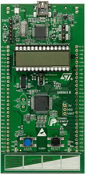
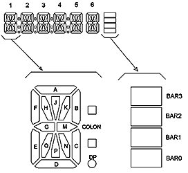
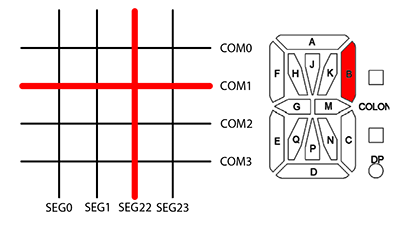
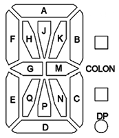
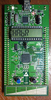
The STM32L-Discovery debug board has a liquid crystal display (LCD, English LCD. Liquid crystal display), which has six 14 segment characters, 4 colon characters (Colon), 4 dots (DP), 4 strips (Bar). All segments are combined into СOM0, COM1, COM2, COM3 groups of 24 segments each. Each group has its own separate “common wire."
The microcontroller STM32L152RBT6 is installed on the debug board. The microcontroller has an integrated LCD controller that controls monochrome LCD indicators.
LCD Controller:
Allows you to configure the refresh rate (frame rate - the frequency with which information is updated on the LCD)
Supports static and multiplex control mode
Supports software contrast setting
Allows the use of several levels of control voltage (up to four)
It uses double buffering, which allows updating data in the LCD_RAM registers at any time of program execution without violating the integrity of the displayed information
LCD controller memory registers
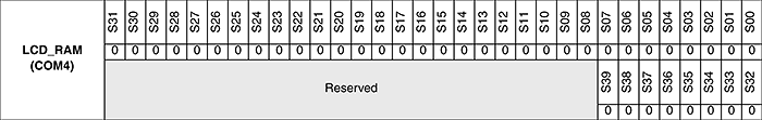
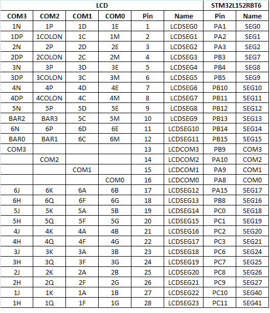
The STM32L152RB microcontroller has special LCD_RAM registers, the information stored in which corresponds to the segment group COM0 - COM3. Each group has two 32-bit registers. Such a number of registers allows the microcontroller to control the LCD with more segments than those installed on the debug board.
To control the LCD with 176 segments, 4 COM0 - COM3 groups of 44 segments each are used; to control the LCD with 320 segments, 8 COM0 - COM7 groups of 40 segments each are used.
The STM32L-Discovery debug board uses an LCD with 96 segments, divided into 4 groups COM0 - COM3 with 24 segments each.
The LCD on the STM32L-Discovery debug board is connected in such a way that bits S40, S41 of the second LCD_RAM registers in each group and bits S0-S27 of the first LCD_RAM registers are used. To reduce the number of registers used, information from bits S40-S43 will be recorded in free bits S28-S31 using the remapping function.
Frequency Divider Block
The frequency divider block (Frequency generator) allows you to achieve different frame rates (frame rates) on the LCD in the range from 32 kHz to 1 MHz. As the source of the clock signal can be used:
32 kHz external low frequency oscillator (LSE. Low speed external)
37 kHz internal low frequency oscillator (LSI. Low speed internal)
External RF generator with frequency dividers of 2.48 and 16 and a maximum frequency of 1 MHz. (HSE. High speed external)
To achieve accurate synchronization and reduce the DC voltage bias across the LCD segments, the clock source must be stable. The LCDCLK clock signal is sent to the LCD controller. The clock frequency is divided in accordance with the division coefficients, which are set by the PS [3: 0], DIV [3: 0] bits of the LCD_FCR register (Frame Control Register). The resulting frequency at the output of the block of frequency dividers is calculated by the formula:
f ck_div = F LCDCLK / (2 PS * (16 + DIV))
The frame frequency is calculated by the formula:
f Frame = f ck_div * duty
where duty is the duty cycle is the ratio of the pulse duration to its period. During one frame, information from the registers LCD_RAM [x], LCD_RAM [x + 1] and so on is sequentially displayed on the LCD. For the LCD installed on the debug board, for one frame, the LCD controller must output information from 4 groups of segments COM0 - COM3, therefore, the duration of the control pulse for one group will be 1/4 of the frame duration, i.e. duty = 1/4.
LCD Management
There are two ways to control the LCD - static control mode and multiplex control mode. With a static indication, each segment of the indicator discharge is connected to the output of the microcontroller. In relation to the LCD, on the STM32LDiscovery debug board, you will need 6 * 14 = 84 pins of the microcontroller (excluding colons, dots and stripes). Due to the use of so many pins, connecting to other peripherals will become impossible. The STM32L152RB microcontroller has 64 pins. In multiplex control mode (dynamic control mode), the same segments of the indicator bits are combined into groups. The information is displayed due to the alternate ignition of the segments of the indicator bits, with a frequency not perceived by the human eye.
Multiplex control allows you to manage a large number of segments. Instead of separately controlling each element, they can be addressed by rows and columns (COM and SEG), thus simplifying the control circuit, because Each segment does not require its own control line. To enable the selected segment, it is necessary to apply the potential difference COM and SEG to it. An example of the operation of the first digit of the indicator (“1:” is displayed on the indicator): The first digit of the indicator at time t 0 The first digit of the indicator at time t 1 The first digit of the indicator at time t 2
General scheme for connecting segments to the
terminals of the LCD to the ports of the microcontroller
For SEG lines, a control voltage is used, the number of levels of which is determined by the bias coefficient. The LCD on the debug board uses the multiplex control mode with duty = 1/4 and bias = 1/3. The values of duty and bias are set via the LCD_CR (Control Register) in bits DUTY [2: 0] and BIAS [1: 0].
Practice
Configuring microcontroller ports
To control the LCD ports of the microcontroller must be configured accordingly:
To the exit
Using the alternative function AF 11 (Alternate function)
Have output frequencies at 400 kHz port
Use push-pull mode
Without pull-up resistors
When the port is in the alternative function mode, the output data buffer of the port is controlled by signals from the periphery. The header file stm32lxx.h of the CMSIS library contains a description of all peripheral registers, as well as their access structure.
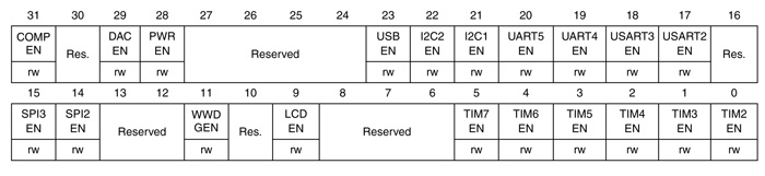
The LCD pins are connected to the GPIOA (PA1-PA3, PA8-PA10, PA15), GPIOB (PB3-PB5, PB8-PB15), GPIOC (PC0-PC3, PC6-PC11) ports of the microcontroller. For the LCD to work, a clock signal must be applied to the selected ports. The clocking of the GPIO ports of the microcontroller comes from the AHB bus of the RCC (Reset and Clock Control) system - the clocking and reset system. The clock signal is supplied by setting the corresponding bits in the RCC_AHBENR (AHB peripheral clock enable register) register. Register RCC_AHBENR (the figure shows the first 15 digits)
For the GPIOA, GPIOB, GPIOC ports, it is necessary to set 1 to 0, 1, 2 bits of the register.
Next, I will cite the code for writing information to the register using bitmasks and using hexadecimal codes. Using bitmasks is more convenient, but working with hexadecimal codes allows you to understand the essence of working with registers.
RCC->AHBENR |=(RCC_AHBENR_GPIOAEN|RCC_AHBENR_GPIOBEN|RCC_AHBENR_GPIOCEN);
или
RCC->AHBENR = 0x7; /* 0x7=111 */
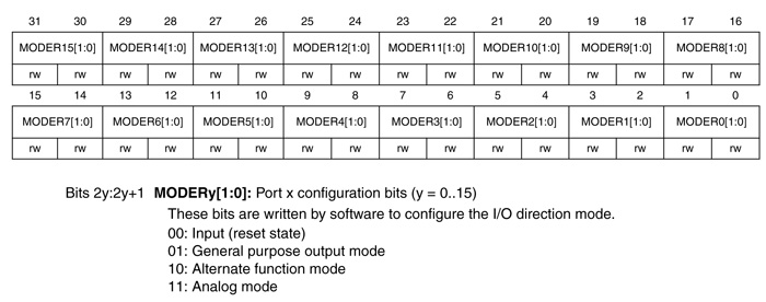
The GPIOx_MODER (GPIO port mode register) register (x = A..H) is used to indicate port operating modes. All register bits are grouped into MODERy groups [1: 0], where y is the pin number of the corresponding port. Ports must be configured for alternative function mode, i.e. in the group responsible for the pin, set the value to 10. For the GPIOA port, you need to configure the pins 1-3.8-10.15, that is, set 1 to 3,5,7,17,19,21,31 bits. GPIOx_MODER register (GPIO port mode register)
The microcontroller ports must be put into push-pull mode. To do this, it is necessary to set 1 in the bits responsible for pins in the GPIOx_OTYPER register (GPIO port output type register). GPIOx_OTYPER register (GPIO port output type register)
Both options affect the selected pins. (For the GPIOA port, pins 1-3.8-10.15 are configured). If you need to put all the pins of the port into push-pull mode, you can write the value in the register:
GPIOA->OTYPER = 0x0;
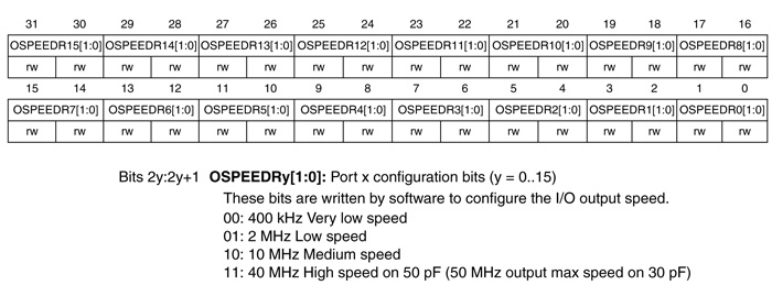
To indicate the frequency of information output to the port, the GPIOx_OSPEEDR (GPIO port output speed register) register is used. All register bits are grouped into OSPEEDRy groups [1: 0], where y is the pin number of the corresponding port. In this work, a frequency of 400 kHz i.e. in the group responsible for the pin, set the value to 00. Register GPIOx_OSPEEDR (GPIO port output speed register)
If you need to set the output frequency to the port 400 kHz for all pins, you can write the value in the register:
GPIOA->OSPEEDR = 0x0;
GPIOx_PUPDR (GPIO port pullup / pull-down register) is used to disable pull-up and pull-down pull-up resistors for selected pins. All register bits are grouped into PUPDRy [1: 0] groups, where y is the pin number of the corresponding port. To disable pull-up resistors in the group responsible for the pin, the value 00 is set. GPIOx_PUPDR register (GPIO port pull-up / pull-down register)
If it is necessary to disable the pull-up resistors for all pins, you can write the value in the register:
GPIOA->PUPDR = 0x0;
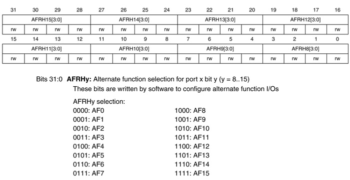
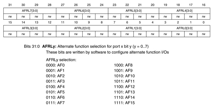
To use the alternative function for the ports of the microcontroller, two registers GPIOx_AFRL (GPIO alternate function low register), which is responsible for low pins (from 0 to 7) and GPIOx_AFRH (GPIO alternate function high register), which is responsible for high pins (from 8 to 15), are used. All bits of the registers are grouped into the groups AFRLy [3: 0] and AFRHy [3: 0], where y is the pin number of the corresponding port. The ports must be configured to use the alternative function AF11, for this, the group responsible for the pin must be set to 1011. Register GPIOx_AFRL (GPIO alternate function low register)
Register GPIOx_AFRH (GPIO alternate function low register)
AFR [0] = 0xBBB0 - writes a value to the GPIOx_AFRL register.
AFR [1] = 0xB0000BBB - writes a value to the GPIOx_AFRH register.
The settings of the corresponding GPIOB, GPIOC port pins are made in the same way.
LCD Controller Setup
When working with the LCD controller, as with other peripherals, it is necessary to apply a clock signal to it. A clock signal is also provided to the power management system. The controller and power management system use the APB1 bus for clocking. To enable clocking in the RCC_APB1ENR register (APB1 peripheral clock enable register), it is necessary to set 1 in the 9th and 28th digits. Register RCC_APB1ENR (APB1 peripheral clock enable register)
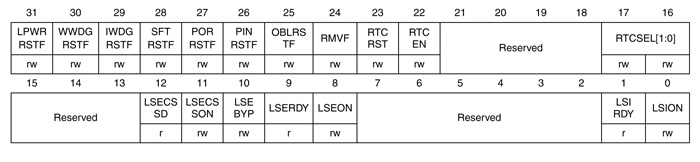
For operation of the LCD controller, it is necessary to indicate the source of clock signals. The source is indicated in register RCC_CSR. By default, writing to this register is prohibited. In the power control register PWR_CR (PWR power control register), write protection in the RCC_CSR register is removed. The RCC_CSR register controls the clock sources of the RTC clock and the LCD controller.
Writing to the RCC_CSR register is enabled by setting 1 to the 8th digit of the PWR_CR register. PWR_CR register (PWR power control register)
To change the clock source of the LCD controller (and the RTC clock too), you must first reset the clock source by setting the RTCRST bit (setting 1 to the 23rd bit) in the RCC_CSR (Control / status register) register. Register RCC_CSR (Control / status register)
RCC->CSR |= RCC_CSR_RTCRST;
Or by writing a value to the register using the operator | | =, because the
default value of the register is different from 0x0:
To select a new clock source, it is necessary to remove the RTCRST bit:
RCC->CSR &= ~RCC_CSR_RTCRST;
или
RCC->CSR &= ~0x800000;
An external bass generator is selected as the clock source. To enable the generator in the RCC_CSR register, it is necessary to set the LSEON bit (set 1 to 8 bit):
After turning on the generator, it takes some time to stabilize it. Generator availability is checked by hardware setting the LSERDY bit in the RCC_CSR register:
while(!(RCC->CSR&RCC_CSR_LSERDY));
The choice of an external LF generator as a clock source is done by setting the value 01 in the RTCSEL [1: 0] group of the RCC_CSR register:
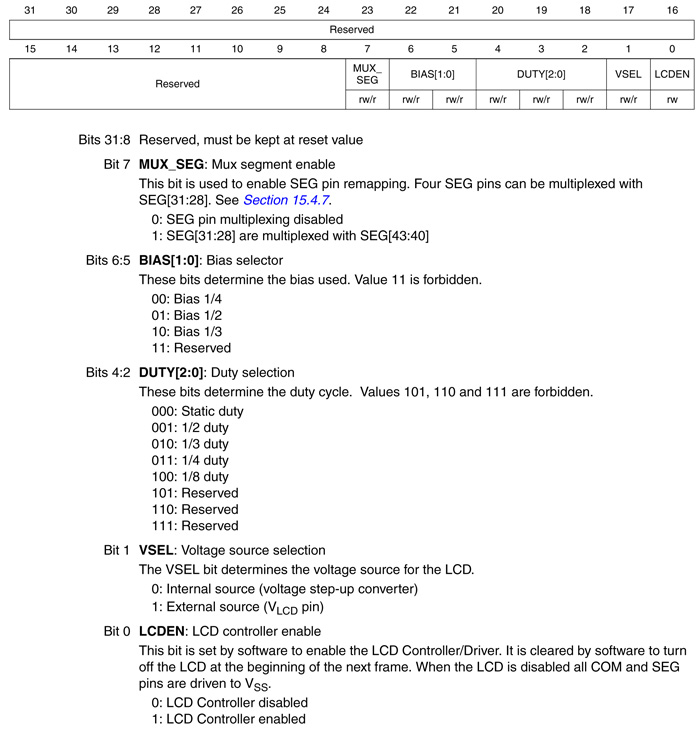
In the LCD controller, you must set the desired bias mode. To do this, in the LCD_CR register (LCD control register), set the value 10 to the BIAS group [1: 0]. Before setting the bits, it is necessary to clear the bits of “garbage”. LCD_CR (LCD control register)
Reset bits:
 LCD->CR &= ~LCD_CR_BIAS;
или
LCD->CR &= ~0x60;
The choice of the bias = 1/3 mode using a bitmask:
LCD->CR |= LCD_CR_BIAS_1;
или
LCD->CR |= 0x40;
Set the duty = 1/4 mode. To do this, first reset all the bits:
LCD->CR &=~LCD_CR_DUTY;
или
LCD->CR &= ~0x1C;
Set the value 011 to the DUTY group [1: 0] of the LCD_CR register for
duty = 1/4 mode:
LCD->CR |= LCD_CR_DUTY_0|LCD_CR_DUTY_1;
или
LCD->CR |= 0xС;
We activate the function of redirection of conclusions. To do this, set 1 in the 7th digit of the LCD_CR register:
LCD->CR |= LCD_CR_MUX_SEG;
или
LCD->CR |= 0x80;
We set the values of the division coefficients of the frequency of the LCDCLK clock signal. Coefficients are set in the LCD_FCR register (LCD frame control register). First, we also clear all the bits, then set the necessary ones. LCD_FCR register (LCD frame control register)
The values of the division coefficients of the clock frequency are set equal to ck_ps = LCDCLK / 16, ck_div = ck_ps / 17. To do this, set 1 to 24 and 18 digits:
To set the desired contrast level, it is necessary to set the value 010 to the CC group [1: 0], also having previously cleared the bits from the old values:
After setting all the values, it takes some time to synchronize the LCD_FCR register. Register synchronization is checked by setting the FCRSF bit in the LCD_SR register (LCD status register). Register LCD_SR (LCD status register)
while(!(LCD->SR&LCD_SR_FCRSR));
As the voltage source for the LCD, select the internal step-up converter to form V lcd . For this, the first digit of the LCD_CR register (LCD control register) is set to 0:
LCD->CR &= ~LCD_CR_VSEL;
или
LCD->CR &= ~0x2;
The operation of the LCD controller is enabled by setting 1 to 0 bit of the LCD_CR register (LCD control register):
LCD->CR |= LCD_CR_LCDEN;
или
LCD->CR |= 0x1;
After installing an internal step-up converter as a voltage source, you must wait for its readiness. Availability is checked by hardware setting the RDY bit in the LCD_SR register (LCD status register):
while(!(LCD->SR&LCD_SR_RDY));
After allowing the operation of the LCD controller, it is necessary to wait for its readiness. Availability is checked by hardware setting the ENS bit in the LCD_SR register (LCD status register):
while(!(LCD->SR&LCD_SR_ENS));
LCD imaging
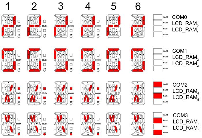
All segments of the indicator are combined into groups COM0 - COM3 with 24 segments each (SEG0-SEG23). Information about the segments is stored in the LCD_RAM registers of the LCD controller memory. The PCB layout is such that the segment numbers do not correspond to the digit numbers of the LCD_RAM registers.
To display 1 in the first digit of the LCD, it is necessary to light up segments 1B, 1C. Segment 1B belongs to group COM0, segment 1C belongs to group COM1. Therefore, information about them should be recorded in the registers RAM [0] (LCD_RAM0), RAM [2] (LCD_RAM2), respectively. For segment 1B, the output of the LCDSEG22 is responsible, information about which is stored in the SEG40 bit of the RAM register [1] (LCD_RAM1). Using the reassignment function, the SEG28 bit of the RAM register [0] (LCD_RAM0) will be responsible for the LCDSEG22 segment. For the segment 1C, the output of the LCD LCDSEG1 is responsible, information about which is stored in the SEG1 category of the RAM register [2] (LCD_RAM2).
Before writing values to the memory registers, it is necessary to check whether the previous data transfer to the LCD is completed. To do this, the UDR (Update display request) bit of the LCD_SR (LCD status register) register is checked. The LCD controller has two output buffers, information is entered into the first buffer, and displayed on the LCD from the second buffer. The UDR bit is set during transmission from the first buffer to the second, protecting the LCD_RAM registers from writing:
while(LCD->SR & LCD_SR_UDR);
After writing information to the LCD_RAM registers, it is necessary to set the UDR bit in the LCD_SR register (LCD status register) (set 1 to 2 bit):