How to hack an expensive camera so that your wife won't kill you
- Transfer
Disclaimer: the study began in 2013, so if you consider some of the methods to be stupid and dangerous, you are right, it was. However, I learned a lot in the process.
Introduction
It all started a few months before the birth of my first child. My wife and I always wanted to buy a cool Leica camera and suddenly realized that if we didn’t buy now, we wouldn’t be able to do it for a long time. Therefore, we ordered the camera M240 and ... boom, we were put in line for six months. Soon I was tired of waiting, and I began to study their site. My attention immediately attracted a section with files. Well, you can guess why ... Firmware!
I saw an unencrypted and uncompressed file (
This is actually very funny, because when I later studied the Leica T compressed firmware file, I first decided to check the compression methods that id Software used in the past.
Wikipedia says they used the LHA format , which is essentially LZW. But the common LZW decompressors did not fit, so I began to look for a specific implementation of the id software - and voila, I found in the source code for Catacomb Armageddon . I must admit, lucky.
Anyway, back to the M8. Here is the firmware structure:
IDA out of the box does not support Blackfin processors, but there is a third-party plugin .
The Leica M9 firmware file (
The end of the story? Maybe not. The fact is that Leica used rather weak processors in the cameras, and at that time XOR encryption was often used in consumer electronics, so I decided to write a simple tool for the XOR operation to compare the firmware with myself and calculate some statistics.
The key length was determined by searching for the longest repeating pattern. This makes sense, since any firmware usually includes large blocks of duplicate data, such as stuffing 0x00 / 0xFF or graphics with LUT pixels. The key itself is calculated by the frequency of bytes within the key length, where the most frequent byte goes to the key buffer. The result of the program clearly indicated XOR encryption. Then I had to modify the tool a bit to get the potential key and decrypt the code. This again turned out to be a PWAD file.
The content of PWAD revealed the following structure:
I got in the habit of checking out the Leica firmware download page every morning. Soon there appeared a new file: FW_M240_1_1_0_2.FW .
It did not look encrypted, but was compressed ...
The histogram shows a huge surge at 0x9D.
Perhaps this is some kind of compression magic. Internet search [9D + compression] gave nothing, except that 0x1F9D is used as the signature of the LZW compression . If that, I understand the types of compression LZ and decided to look at the bytes after 0x9D. And I saw four options:
What else managed to notice:
From what I know about LZ, this is very similar to LZ77 or LZSS, where YY is the indent step, and XX is the number of bytes to copy. And the second option is a special case of issuing 0x9D. I wrote a simple C function that implements this logic. She confirmed that we are moving in the right direction, but the fourth option still does not fit into the scheme.
I tried to interpret it in every possible way, but nothing happened. Therefore, I turned to my comrades for advice. One guy noticed that, according to my own observations, the fourth byte YY only appears when the highest bit 0x8Y is set: this is just an extra distance for the indent pitch. I was ashamed, everything turned out so obvious ...
Finally, the decompressor began to issue a valid stream ... until it got stuck in the middle of the file. This was due to the unknown length of the sliding window. Additional debugging and tests fixed the situation.
This is how the tool for parsing firmware M240 appeared .
To work with an unknown format, I didn’t come up with anything better than to measure some of the offsets and sizes of sections of code — and try to find the closest values in the file header. For example, this unit: eventually turned into: As I understood the structure of the firmware, I improved my tool, and ultimately it produced this: M240 firmware includes one container with nine elements: As you can see, in one firmware there are two sets of files. Later I found out that the 212 is a version of the image processing microchip, and two versions of the Leica M240 went into production. This study is based on version 212.
The only common part is the firmware for the system management chip. This is a really big binary, and it is not difficult to guess from the code what it is intended for. Thus, we have the Renesas SH7216 (SH-2A) processor, which is responsible for the early loading stage, I / O tests, and firmware updates. IDA out of the box supports this type of processor. It only remained to find the correct base boot address, known from the description of the sections of the firmware: this . I downloaded it in IDA and recognized all the functions, but I didn’t dig in it especially because the firmware of the main processor is much more interesting. Here you can also note that the UART of this chip opens on the service port, where it issues a download log. We will come back to this later.
To start reverse engineering this firmware, you must first answer a few questions:
Thanks to our tool, we already know the base load address: this
The reality was not so bright, because after downloading the firmware file, the IDA program did not show any instructions, external links, etc.
I decided to fix it, but in the end I had to completely rewrite some parts of the firmware . Here is the result:


In addition to the corrections in
But the biggest change, as you noticed, is upper case letters for instructions :)
Want to see the full set of instructions? Here he is:
Just like that, simple and beautiful.
By the way, you may have noticed that some instructions are not aligned:
This is not an error in the processor module, but in fact a feature of the Fujitsu FR family. It is called the slot delay and is quite typical for RISC processors.
From the FR80 processor manual (note: the link no longer works):
Thus, it is, in fact, the optimization of the pipeline, and it is better to remember about it, because it is used everywhere in the Leica firmware.
From wiki :
So this is a pretty popular decent RTOS with tasks, semaphores and other goodies. I was wondering if you can recognize some standard library functions in the Leica firmware.
I must name the first part of the study as a great waste of time, and here's why.
Softune IDE turned out to be very difficult to find, but in the end I managed to get something. As expected, the IDE included libraries. There were four binary files:
I do not know why, maybe by inertia, as I cracked everything connected with Leica, I again began to reverse-engineer the format. Yes, a very well documented Object Module Format . And yes, of course, I wrote a special tool for this : You can use it to create files and use them as input to IDA FLAIR to generate signature files . After applying this signature, I was finally happy to see the correspondences in IMG_LOKI-212.idb .
Immediately draws attention to the number of lines in the firmware. Many functions are named for their functionality. This is very useful in the reverse engineering process to understand the overall pattern.
It is also important to note that some parts of the firmware file are copied to another address in the reset handler. For example, the built-in loader at run time moves higher in memory.
I had to manually create additional partitions, this resulted in the following layout:

The interrupt vector table can be found by accessing the TBR (Table Base Register): It usually occurs in the vector reset handler at the very beginning of the firmware. Handler addresses in the table are stored in the reverse order of the formula , so that the reset vector at the end of the table is offset . I found most of the interrupts from the FR manual and suggested that Leica Maestro has a similar layout. Then he took each handler and tried to find a string or any other hint revealing the purpose of the interruption. As a result, I made the following list: Many interrupts are quite expected, such as AUDIO / SDIO / VIDEO / JPEG / RAW, but try to determine the most mysterious of them? I'm talking about interruption . It seems that the camera supports some kind of console mode UART CLI.
Like almost any OS, Softline REALOS uses system calls. In assembly language, they look like this: The
actual address of the system call handler is calculated as follows. Let's start by looking for an interrupt handler
easy to find a reference in the handler to the bottom of the system call table with 16-bit words. The specific entry in this table is calculated by the formula
This does not look like an address, because the actual address of the system call handler is calculated as
All system calls and their functionality are listed in the Softline REALOS / FR Core Guide.so I was able to restore all the implemented handlers in the table and further improve the IDB.

Of course, you can make the code even more beautiful by defining the types of system calls in IDA.

I wrote a Python script to automatically search for these system calls and so on.
In the system call,
At the very beginning we see some links. I had to tinker with the data types, but in the end the parts came together:
and so on. Only 15 tasks. It was a matter of time to look into each main function, to determine the name and purpose of the task (except for the last). Here is the complete list:
It is interesting to note that after the main array there is another outstanding descriptor. And the task function is simply branching itself. This handle is referenced at the end of the function , which is responsible for creating other tasks and setting up the firmware. So this is most likely the task of inactivity of the system.
In addition to tasks, you can define some logical objects, such as IO and peripheral modules. Modules are presented as a group of message handlers in one of the tasks.
The IO group seems to include:
And in the peripheral group:
The messaging system itself uses standard SOFTUNE structures:
As expected, IPC also has several message groups. Since many messages are processed in tasks and modules, I was able to restore only some of these groups:
Unfortunately, many other messages remain unknown.
In the firmware file, let's look at the following sections: CTRL_SYS-11 , IMG-LOKI-212 , IMG-DSP-212 , IMG-FPGA-212 and IMG-LENSDATA-212 .
What surprised me was the complete lack of GUI resources. But they must be somewhere and, most likely, embedded in IMG-LOKI-212 .
One of my usual approaches to reverse firmware development is to restore all possible cross-references. Not only in the code, but also in the data section. Then I look at them, trying to find some patterns or links to known parts of the code.
Leica firmware is no exception. There are many similar data sequences with addresses to other data sequences that go further, and so on. Going up the link hierarchy, I finally saw a familiar function.
For example, I found a data structure without any references:
She was addressed by another structure:
Which in turn is addressed by another structure:
This data structure has a link from the code, and it is passed as a parameter to another function:
However,
Having looked above, I found a call in the code
Again, this function is stored in an array:
Some other code refers to the array itself:
Fortunately, this time the function is called from another function, and so on
Some lines indicate that the GUI subsystem is called “MADE”, and page transitions are processed using

As you can see, the main function for GUI resources is
There are four types of resource descriptions:
The first type has a header with a link to an array of records. Each entry has the coordinates and address of the pixel data. The current type seems to describe state-dependent elements, such as icons, which can be grayed out or disappear from the UI.
The second type also starts with a header and is used for localization, description of lines or blocks of text.
The third type describes character maps for different languages.
The latter type is responsible for all other static resources, such as images, backgrounds, etc.
Now, take a look at the data for images themselves. The first six bytes look like a small header, followed by some kind of repeating pattern, where every second byte is either or . It is logical to assume that and
Looking at this hex dump, it's hard to believe that some complicated scheme is being used. Leica's GUI is not very colorful, so in my experience it’s best to use the LUT table. In this case, the UI resources will completely repeat the LUT indexes like
With all this in mind, I assumed that there was most likely a simple image with two colors LUT (
“And then you wrote another tool,” you think. But no, I took a pen and paper and began to fill the cells. It's funny that I still have that picture.
Somewhere along the way, I realized that 160 pixels is not enough for this image, so 0x8 and 0x14 need to be multiplied by two. The third word 0x0001 indicates whether the image is an ASCII character, so the final ImageAsset structure is as follows:
But one part is still missing: LUT.
It was not so difficult to find, because many links and structures were already manually restored, so I slowly scrolled through the data sections, looking for an array of 256 elements from 16-bit or 32-bit values, until I came across this: Again, thanks In my work with Blackmagic Design, I immediately recognized the YUV pixels (for example, all values with 8080 digits). I'm not stupid to draw the whole user interface again on paper, so yes, I wrote another tool - M240UITool . In addition to resetting all image resources from a firmware file to BMP / PNG, this tool can create IDC scripts in IDA to determine all UI resources.
We already know that from the function that one UI page creates, it is called several times
And who said that the UI resource browser might not look unusual?

Being interactive (translucent buttons on the screenshot), this tool allows you not only to scroll through the EVF / LCD menu pages, but also to view the rendering steps within one page.
Unfortunately, the source code of this masterpiece is lost somewhere, but the header files are still in the M240UITool code, so you can technically recreate it from scratch.
What line are we looking for in the first place during reverse engineering? In my opinion, this word
The firmware had a lot of interesting lines, but these are special: It seems that you can enter debug mode using some kind of key combination. All of these lines are called from a single giant function that implements a button-scanning state machine. Here’s what it looks like in IDA:

I will not lie, it took some time to understand how the hardware buttons are processed in the firmware, and then to restore the enumerated types for the buttons and the joystick. But when I got the combination, I found out with distress that she was not doing anything. It probably works only from a specific GUI page. A couple of evenings of manual tracing of the GUI state machine - and the problem was solved, and the Reset menu page was also found.
Finally, welcome to debug mode.

I thought a lot, whether to announce this combination, but decided to abstain. I respect the hard work that Leica does when releasing its unique devices, and I don’t want to be responsible for the fact that their service centers fill in broken carcasses of cameras as a result of some thoughtless curiosity.
But still, I will provide some enumerated types in order to simplify reverse engineering for those who are ready to follow this path.
Thinking over the USB task, I defined three modes (which is also confirmed in the debug menu):
PTP is most interesting because it is well documented and allows you to control the camera.
It is quite easy to find PTP handlers in the firmware, because there are a lot of calls from this code. All PTP calls are divided into three groups: Legacy , Leica Extended (LE) and Production .
Debug messages helped to set titles for almost the entire code.
The implementation of the PTP interface itself seems standard, but some commands have limitations, which I intentionally omit here.
In any case, all of the above is quite fascinating. You might think, "Let's just connect the camera via USB and start probing using libptp." That's right.
Only damn ...
The Leica M240 does not have a USB port.
Leica offers some accessories for this camera, but there is one particularly interesting. This is a multi-function handle Leica M (14495) . It replaces the lower metal part of the body, provides a built-in GPS and several connectors like USB, a SCA flash terminal, DIN / ISO-X and a power jack.

And again you will say: “Great, now just buy it, attach it to the camera, connect the camera via USB and start probing with the help of libptp”. That's right.
Only damn ...
It costs almost $ 900.
This is almost nine hundred reasons to create your own adapter. However, just in case, I set up eBay notifications for this accessory.
The connector on the camera looks like this:

I tried to find it on the Internet, but seriously, how would you describe it in Google?
A little desperate, I started thinking about some crazy things, like sticking foil or needles to a rubber eraser. But once at work in Blackmagic Design, looking at the printed circuit board of the camera, I noticed that one connector had a very familiar shape. The next day I brought my Leica M240 to work - and yes, it looked similar, just much longer with more contact pads.
It remains to ask the part number from our component manager, and then find it in the Samtec catalog: ERM8-013-05.0-L-DV-TR .

We also asked Samtec representatives if a sample could be obtained, and they kindly agreed.

A bit of work with a soldering iron, cardboard and electrical tape - and my own plug is ready (sample 2013).

Five years later, in 2018, I decided to personally ask Samtec to send another sample. I wanted to do something better.
ERCD-013-05.00-TTR-TTR-1-D

Again, a lot of work with a soldering iron, swearing, cutting the wire, swearing, again working with a soldering iron to make a new, more attractive option:

In the connector 26 contacts: 13 on each side. Even before soldering my part, I probed the camera connector with a multimeter and a logic analyzer. By the way, you need to put a magnet on the bottom cover sensor so that the camera thinks that the cover is in place.
Earth (camera off, no battery)
I always start from the ground because it is safe and very easy to find.

Thus, we have eight ground lines (dark gray).
Potential (camera on)
When the camera is on, you can measure the potential at each contact and get an idea of the logic and power levels.
alexhude.github.io/assets/2019/2019-01-24-hacking-leica-m240/probe2_potential.png
The numbers on pins 8-9 and 11-13 are too high for logical contacts, so I defined them as power (red).
Resistance (camera off, no battery)
It is also useful to measure resistance. In some cases, it helps to identify entrances and group some lines.

Connected outputs (camera off, no battery)
Then I decided to check all external pads on the camera body to check if they are connected to the service port.

The flash sync switch was directly connected to line 10.
Logic analyzer (camera turned on) The
data for each line was recorded in the following sequence: turn on, the camera should be in LV mode, take a picture, start video recording.

Two lines show the transfer of some data: 01 and 21.
01 - 115200, transmission of 8 bits, 1 stop bit, parity bit, LSB first.

Every 500 ms, it sends some kind of counter
21 - 115200, 8-bit transmission, 1 stop bit, no parity bit, first LSB.

It sends the SH7216 bootloader log (“Leica Camera AG” in the screenshot above).
Let's mark them dark blue. It is rather sad that the Maestro log does not give out even with the maximum debugging settings in the Debug menu.

At these contacts, the resistance is about 310kOhm.
I do not know why, but I assumed that other data lines may have similar resistance or will be closed. Therefore, I defined ~ 300kOhm, ~ 200kOhm and ~ 100kOm lines as data lines as well (shades of blue in the figure).
In general, the following picture was drawn.

12 candidates for data lines. But how to check them? After a brief conversation with the hardware experts about the electrical protection of integrated circuits, I started poking at the contacts through a 4kOhm resistor, reducing the current to a level that should not burn the inputs.
I made another assumption that the line RX should be next to the TX. Lines 02, 03 and 20 look like good candidates, because both have 3.3 V voltage like TX.
Initially, I tried to explore these lines using the Bus Pirate. Unfortunately, the result was pretty messy. Then I took the SiLabs based cables as more reliable and non-conflicting with macOS.
First, I connected the TX cable to pin 20 and started dialing

Contacts 02 and 03 were the next UART candidates. Unfortunately, there were no signs that these lines are tapped.
On the diagram, the famous UARTs are indicated by a darker shade of green.

It all started with a cut USB cable in half with a header in the middle and 4kOhm resistors for sensing. Signal integrity of a differential pair? Nope, then it didn't really bother me. :)

Then I sounded at home several household devices with USB to get an idea of what the communications on this port looked like.
Canon

camera Blackmagic pocket camcorder

Canon

camcorder JVC camcorder

Keyring

KidiZoom camera

They are all a little different, but the initial state of D-D + is low. Well, we will know, and now we will check that we have:
So I connected the USB D-D + to the pins 15/16 and connected to the iMac ...

On the USB PTP screen, but the camera did not appear on the host. I tried to configure different options on the layout of the electronic scheme, but nothing worked. Beagle showed a lot of damaged packages and other errors. In the end, I gave up and went back to reverse engineering the firmware.
This is the final pinout, USB is marked in dark green.

Who would have thought that a few years later, that eBay notification would come to me and I would rather cheaply buy the desired accessory.
Finally, I can check my assumptions about PTP. But at first it was very curious how the USB PHY looks inside the gadget.

Inside was the hub SMSC 2512bRight on the road from the grip connector to the Mini USB connector. The chip works in default mode, because there is no EEPROM or SCL / SDA pins. The first downstream port is routed to the socket of the camera body, but the second is not connected to anything.
Probably, I missed something, but for me such a decision does not make much sense. The technical data sheet says that the chip has “fully integrated USB leads, and also has resistors for boosting and lowering the voltage.” Perhaps Leica’s engineers decided not to implement their own USB PHY, but used the one in the hub, which is well tested and works out of the box. In fact, I can not blame them, because before I tried to do this, and it turned out to be a daunting task. Maybe this is a feature to protect against forgery, who knows.
In any case, if you understand USB PHY and are ready to help, do not hesitate to write to me: it should be possible to work through the USB port without this branded accessory :)
As I said, it's time to play around with the Leica PTP extension.
Fortunately, I found a pretty cool C ++ library instead of libptp - this is libEasyPTP . It also didn't take long to write a tool based on this library: I already knew some limitations in the Leica PTP interface.
And although M240PTPTool is pretty buggy, it is quite suitable for the role of proof of concept ( program code ).
There are only two requests for PTP: GetDebugBuffer (0x900C) and DebugCommandString (0x900D) . By the way, in order for the modules to fill in the debug log, you need to set the Debug Level in the menu as “Debug” or “Debug RAW”.
There are several options in the M240PTPTool interface:
Any other text is sent to the camera as a debug command. For example, it

Then remove the SD card and check what is on it.

Here it is, a complete dump, including the firmware.
This opens up endless possibilities. For example, you can make a tiny device with an MCU, USB host support and buttons to launch complex message sequences ...
And then we had a second child. :)
If you do not want to break the device, there is usually a way to examine it without opening the case or soldering the wires to the circuit board. Below are my tips if you're interested:

github.com/alexhude
Good luck to you hacks!
Introduction
It all started a few months before the birth of my first child. My wife and I always wanted to buy a cool Leica camera and suddenly realized that if we didn’t buy now, we wouldn’t be able to do it for a long time. Therefore, we ordered the camera M240 and ... boom, we were put in line for six months. Soon I was tired of waiting, and I began to study their site. My attention immediately attracted a section with files. Well, you can guess why ... Firmware!
I saw an unencrypted and uncompressed file (
m8-2_005.upd) that starts with the magic of PWAD. Do you recognize? Yes, all right, this is the format of Doom Patch WAD. It seems the guys love the classics. The format is very well documented , so parsing it turned out to be a snap.Leica firmware files
Leica M8 firmware
This is actually very funny, because when I later studied the Leica T compressed firmware file, I first decided to check the compression methods that id Software used in the past.
Wikipedia says they used the LHA format , which is essentially LZW. But the common LZW decompressors did not fit, so I began to look for a specific implementation of the id software - and voila, I found in the source code for Catacomb Armageddon . I must admit, lucky.
Anyway, back to the M8. Here is the firmware structure:
RULES: 0x0000008C (3036: 0x00000BDC) - XML Description LUTS: 0x00000C68 (183274: 0x0002CBEA) GAMMA: 0x0000007C (31760: 0x00007C10) GAIN: 0x00007C8C (50344: 0x0000C4A8) LEICA: 0x00014134 (7000: 0x00001B58) BLEMISH: 0x00015C8C (250: 0x000000FA) WREF: 0x00015D88 (82480: 0x00014230) OBJ: 0x00029FB8 (11268: 0x00002C04) VERSION: 0x0002CBBC (46: 0x0000002E) PXA: 0x0002D854 (858384: 0x000D1910) BF: 0x000FF164 (134522: 0x00020D7A) - Analog Devices Blackfin processor family GUI: 0x0011FEE0 (3574180: 0x003689A4) TRANS: 0x0000005C (59988: 0x0000EA54) - localization IMAGES: 0x0000EAB0 (267433: 0x000414A9) 21_1PRT: 0x000000CC (18411: 0x000047EB) - JFIF image 21_2GRP: 0x000048B8 (23172: 0x00005A84) - JFIF image 21_3PAN: 0x0000A33C (23034: 0x000059FA) - JFIF image 24_1PRT: 0x0000FD38 (18489: 0x00004839) - JFIF image 24_2GRP: 0x00014574 (23230: 0x00005ABE) - JFIF image 24_3PAN: 0x0001A034 (22998: 0x000059D6) - JFIF image 28_1PRT: 0x0001FA0C (22605: 0x0000584D) - JFIF image 28_2GRP: 0x0002525C (23081: 0x00005A29) - JFIF image 28_3PAN: 0x0002AC88 (23282: 0x00005AF2) - JFIF image 35_1PRT: 0x0003077C (22496: 0x000057E0) - JFIF image 35_2GRP: 0x00035F5C (23532: 0x00005BEC) - JFIF image 35_3PAN: 0x0003BB48 (22881: 0x00005961) - JFIF image FONT1: 0x0004FF5C (1522988: 0x00173D2C) FONT2: 0x001C3C88 (1723676: 0x001A4D1C) VERSION: 0x003689A4 (0: 0x00000000) M16C: 0x00488884 (130406: 0x0001FD66) - Renesas M16C Family (Motorola S-record) FPGA: 0x004A85EC (131604: 0x00020214) - Xilinx Spartan 3 FSL: 0x004C8800 (814: 0x0000032E) - the first stage loader
IDA out of the box does not support Blackfin processors, but there is a third-party plugin .
Leica M9 Firmware
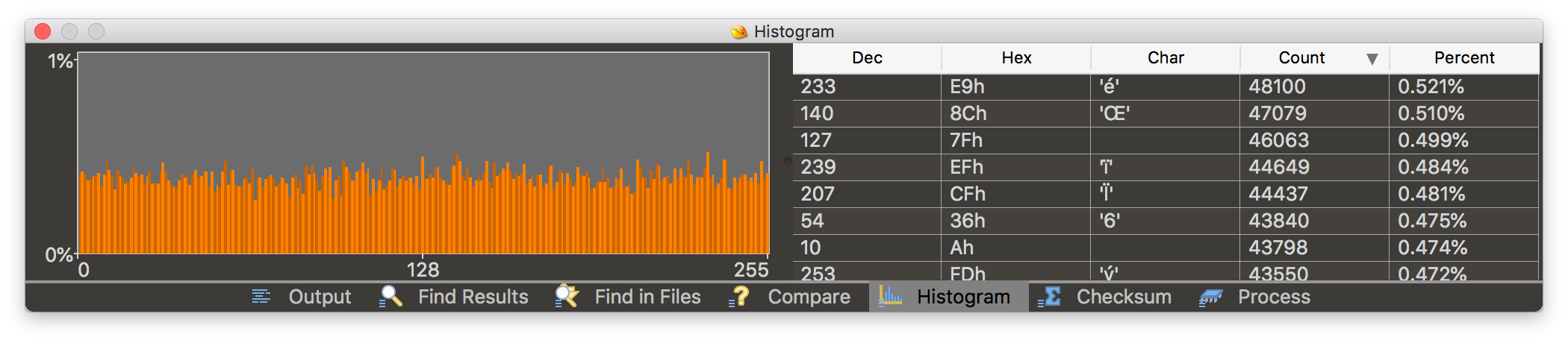
The Leica M9 firmware file (
m9-1_196.upd) looks encrypted: a histogram shows a distribution of about 0.45%. The end of the story? Maybe not. The fact is that Leica used rather weak processors in the cameras, and at that time XOR encryption was often used in consumer electronics, so I decided to write a simple tool for the XOR operation to compare the firmware with myself and calculate some statistics.
The key length was determined by searching for the longest repeating pattern. This makes sense, since any firmware usually includes large blocks of duplicate data, such as stuffing 0x00 / 0xFF or graphics with LUT pixels. The key itself is calculated by the frequency of bytes within the key length, where the most frequent byte goes to the key buffer. The result of the program clearly indicated XOR encryption. Then I had to modify the tool a bit to get the potential key and decrypt the code. This again turned out to be a PWAD file.
The content of PWAD revealed the following structure:
RULES: 0x0000007C (2788: 0x00000AE4) - XML Description LUTS: 0x00000B60 (4060616: 0x003DF5C8) PROCESS: 0x0000004C (3900572: 0x003B849C) CREATE: 0x0000004C (20: 0x00000014) - time stamp LUTS: 0x00000060 (427744: 0x000686E0) GAINMAP: 0x00068740 (20008: 0x00004E28) LENS: 0x0006D568 (3452724: 0x0034AF34) CCD: 0x003B84E8 (148662: 0x000244B6) CREATE: 0x0000004C (20: 0x00000014) - time stamp BLEMISH: 0x00000060 (1092: 0x00000444) WREF: 0x000004A4 (147452: 0x00023FFC) LIN: 0x000244A0 (22: 0x00000016) ICCPROF: 0x003DC9A0 (4304: 0x000010D0) ECI-RGB: 0x0000003C (540: 0x0000021C) sRGB: 0x00000258 (3144: 0x00000C48) A-RGB: 0x00000EA0 (560: 0x00000230) WBPARAM: 0x003DDA70 (7000: 0x00001B58) BF561: 0x003E0128 (289128: 0x00046968) - Analog Devices Blackfin Processor family bf0: 0x0000004C (117846: 0x0001CC56) - the main processor bf1: 0x0001CCA4 (117826: 0x0001CC42) - Subprocessor firmware bf0.map: 0x000398E8 (27072: 0x000069C0) - main processor firmware card with characters: D bf1.map: 0x000402A8 (26304: 0x000066C0) - subprocessor firmware card with characters: D BODY: 0x00426A90 (143280: 0x00022FB0) - Renesas M16C Family (Motorola S-record) GUI: 0x00449A40 (3647624: 0x0037A888) TRANS: 0x0000005C (131656: 0x00020248) - localization IMAGES: 0x000202A4 (267433: 0x000414A9) 21_1PRT: 0x000000CC (18411: 0x000047EB) - JFIF image 21_2GRP: 0x000048B8 (23172: 0x00005A84) - JFIF image 21_3PAN: 0x0000A33C (23034: 0x000059FA) - JFIF image 24_1PRT: 0x0000FD38 (18489: 0x00004839) - JFIF image 24_2GRP: 0x00014574 (23230: 0x00005ABE) - JFIF image 24_3PAN: 0x0001A034 (22998: 0x000059D6) - JFIF image 28_1PRT: 0x0001FA0C (22605: 0x0000584D) - JFIF image 28_2GRP: 0x0002525C (23081: 0x00005A29) - JFIF image 28_3PAN: 0x0002AC88 (23282: 0x00005AF2) - JFIF image 35_1PRT: 0x0003077C (22496: 0x000057E0) - JFIF image 35_2GRP: 0x00035F5C (23532: 0x00005BEC) - JFIF image 35_3PAN: 0x0003BB48 (22881: 0x00005961) - JFIF image FONT1: 0x00061750 (1522988: 0x00173D2C) USBLOGO: 0x001D547C (1775: 0x000006EF) - JFIF image FONT2: 0x001D5B6C (1723676: 0x001A4D1C) FPGA: 0x007C42C8 (150176: 0x00024AA0) - Xilinx Spartan 3A BF547: 0x007E8D68 (937576: 0x000E4E68) - Analog Devices Blackfin processor family (FSL?)
Leica M240 firmware
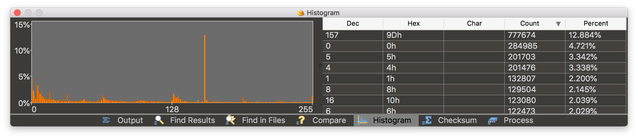
I got in the habit of checking out the Leica firmware download page every morning. Soon there appeared a new file: FW_M240_1_1_0_2.FW .
It did not look encrypted, but was compressed ...
Compression
The histogram shows a huge surge at 0x9D.
Perhaps this is some kind of compression magic. Internet search [9D + compression] gave nothing, except that 0x1F9D is used as the signature of the LZW compression . If that, I understand the types of compression LZ and decided to look at the bytes after 0x9D. And I saw four options:
9D 70 C49D 009D XX YY9D XX 8Y YY
What else managed to notice:
- the first option pops up only once at 0x30: probably used as an indicator of compressed data;
- XX never exceeds 0x7F;
- the last byte of YY in the third and fourth cases never exceeds 0x7F
From what I know about LZ, this is very similar to LZ77 or LZSS, where YY is the indent step, and XX is the number of bytes to copy. And the second option is a special case of issuing 0x9D. I wrote a simple C function that implements this logic. She confirmed that we are moving in the right direction, but the fourth option still does not fit into the scheme.
I tried to interpret it in every possible way, but nothing happened. Therefore, I turned to my comrades for advice. One guy noticed that, according to my own observations, the fourth byte YY only appears when the highest bit 0x8Y is set: this is just an extra distance for the indent pitch. I was ashamed, everything turned out so obvious ...
Finally, the decompressor began to issue a valid stream ... until it got stuck in the middle of the file. This was due to the unknown length of the sliding window. Additional debugging and tests fixed the situation.
This is how the tool for parsing firmware M240 appeared .
Firmware structure
To work with an unknown format, I didn’t come up with anything better than to measure some of the offsets and sizes of sections of code — and try to find the closest values in the file header. For example, this unit: eventually turned into: As I understood the structure of the firmware, I improved my tool, and ultimately it produced this: M240 firmware includes one container with nine elements: As you can see, in one firmware there are two sets of files. Later I found out that the 212 is a version of the image processing microchip, and two versions of the Leica M240 went into production. This study is based on version 212.
0x00: 1E 1C AF 2E 01 01 00 02 07 E1 EA 5E 00 5C 1A B1

0x10: 01 29 1A 7E AE 38 73 65 9C 3D 75 B4 34 2F 44 6E

0x20: 13 17 8E 6B 00 00 00 01 00 00 00 30 E1 E3 50 D1
1E1CAF2E — выглядит как "LEICA FILE"
01010002 - 1.1.0.2
005C1AB1 — размер сжатого файла (big endian)
01291A7E — размер несжатого файла (big endian)
AE3873659C3D75B4342F446E13178E6B — хэш MD5
00000001 — количество полезных нагрузок
00000030 — смещение первой полезной нагрузкиRunning with options:
+ firmware folder: M240_FIRMWARE
+ verbose enabled
Open firmware file: FW_M240_1_1_0_2.FW
File size: 6036193 | 0x005C1AE1
Parse container header:
version: 1.1.0.2
packed size: 6036145 | 0x005C1AB1
unpacked size: 19470974 | 0x01291A7E
body blocks: 1 | 0x00000001
body offset: 48 | 0x00000030
MD5: AE387365 9C3D75B4 342F446E 13178E6B
MD5 check: PASSED
Uncompress container body:
6036145 -> 19470974
Uncompression: DONE
Split container:
Number of sections: 9 | 0x00000009
Section table size: 612 | 0x00000264
Section table offset: 36 | 0x00000024
Section 1
Section Name: "[A]IMG_LOKI-212"
Section offset: 0 | 0x00000000
Section size: 7340032 | 0x00700000
Section base: 1048576 | 0x00100000
MD5: A8D55AA2 B0ACDB14 0673AD79 707674F3
MD5 check: PASSED
Create file: M240_FIRMWARE/IMG_LOKI-212.bin
~~~~~~~~~~~~~~~~~~~~~~~~~~~~~~~~~~~~~~~~~~~~~~~~
Section 9
Section Name: "[A]IMG-LENSDATA-213"
Section offset: 19214844 | 0x012531FC
Section size: 255478 | 0x0003E5F6
Section base: 16252928 | 0x00F80000
MD5: 39C2BEC0 27ED23F6 2C1C8513 EEE697B9
MD5 check: PASSED
Create file: M240_FIRMWARE/IMG-LENSDATA-213.bin
Splitting container: DONE
Extraction COMPLETE!IMG_LOKI-212.bin - прошивка прикладного процессора
IMG_LOKI-213.bin - прошивка прикладного процессора
CTRL_SYS-11.bin - прошивка процессора ввода-вывода
IMG-FPGA-212.bin - прошивка для обработки изображений (сенсор)
IMG-FPGA-213.bin - прошивка для обработки изображений (сенсор)
IMG-DSP-212.bin - прошивка DSP
IMG-DSP-213.bin - прошивка DSP
IMG-LENSDATA-212.bin - данные по оптике
IMG-LENSDATA-213.bin - данные по оптикеSystem Management: CTRL_SYS-11.bin
The only common part is the firmware for the system management chip. This is a really big binary, and it is not difficult to guess from the code what it is intended for. Thus, we have the Renesas SH7216 (SH-2A) processor, which is responsible for the early loading stage, I / O tests, and firmware updates. IDA out of the box supports this type of processor. It only remained to find the correct base boot address, known from the description of the sections of the firmware: this . I downloaded it in IDA and recognized all the functions, but I didn’t dig in it especially because the firmware of the main processor is much more interesting. Here you can also note that the UART of this chip opens on the service port, where it issues a download log. We will come back to this later.
$ strings CTRL_SYS-11.bin | rg SH

-> Test SH7216 data flash driver

-> Test SH7216 SCI driver

-> Test SH7216 I2C driver

-> Test SH7216 MTU2 driver

-> Test SH7216 ADC functions

-> Test SH7216 CMT driver0x0Section Name: "[A]CTRL_SYS-11"
Section offset: 14680064 | 0x00E00000
Section size: 917277 | 0x000DFF1D
Section base: 0 | 0x00000000The main chip: IMG_LOKI-212.bin
To start reverse engineering this firmware, you must first answer a few questions:
- what type of processor
- what is the base load address
- what OS is it based on, if any
Thanks to our tool, we already know the base load address: this
0x100000.
The rest of the answers the firmware stores in a readable form. For example, this line:
Thus, we are dealing with a custom processor Fujitsu FR (Leica calls it Maestro ) and Softune REALOS . In fact, it is much better than Blackfin, because IDA out of the box supports FR.Section Name: "[A]IMG_LOKI-212"
Section offset: 0 | 0x00000000
Section size: 7340032 | 0x00700000
Section base: 1048576 | 0x00100000$ strings ./IMG_LOKI-212.bin | rg Softune
6Softune REALOS/FR is Realtime OS for FR Family, based on micro-ITRON COPYRIGHT(C) FUJITSU LIMITED 1994-1999
...FR processor module
The reality was not so bright, because after downloading the firmware file, the IDA program did not show any instructions, external links, etc.
I decided to fix it, but in the end I had to completely rewrite some parts of the firmware . Here is the result:
In addition to the corrections in
ana, insand out, a completely new code emucan:- recognize different types of code and external references to data;
- recognize switch statements;
- perform stack tracing;
- separate stack arguments and local variables;
- correctly recognize the function.
But the biggest change, as you noticed, is upper case letters for instructions :)
Want to see the full set of instructions? Here he is:
ADD OR BTSTH LSR MOV BN LDRES EXTSH
ADD2 ORH MUL LSR2 JMP BP STRES EXTUH
ADDC ORB MULU ASR CALL BV COPOP SRCH0
ADDN EOR MULH ASR2 RET BNV COPLD SRCH1
ADDN2 EORH MULUH LDI INT BLT COPST SRCHC
SUB EORB DIV0S LDI INTE BGE COPSV LDM0
SUBC BANDL DIV0U LDI RETI BLE NOP LDM1
SUBN BANDH DIV1 LD BRA BGT ANDCCR STM0
CMP BORL DIV2 LDUH BNO BLS ORCCR STM1
CMP2 BORH DIV3 LDUB BEQ BHI STILM ENTER
AND BEORL DIV4S ST BNE DMOV ADDSP LEAVE
ANDH BEORH LSL STH BC DMOVH EXTSB XCHB
ANDB BTSTL LSL2 STB BNC DMOVB EXTUB
Just like that, simple and beautiful.
By the way, you may have noticed that some instructions are not aligned:
   BRA: D loc_xxx
    Ldi: 8 # 0x64, R5
This is not an error in the processor module, but in fact a feature of the Fujitsu FR family. It is called the slot delay and is quite typical for RISC processors.
From the FR80 processor manual (note: the link no longer works):
The instruction, which is located immediately after the branch instruction (its location is called the “delay slot”), is executed before the branch, and the instruction on the target address is executed after the branch. Since the instruction in the delay slot is executed before the branch operation, the apparent execution speed is 1 cycle.
Thus, it is, in fact, the optimization of the pipeline, and it is better to remember about it, because it is used everywhere in the Leica firmware.
Softune REALOS
From wiki :
Softune is the Fujitsu integrated development environment for Fujitsu FR, FR-V and F2MC processor families. Powered by REALOS µITRON Real-Time Core. For example, used in Nikon digital SLR cameras (see Nikon EXPEED) and some Pentax cameras with a K bayonet.
So this is a pretty popular decent RTOS with tasks, semaphores and other goodies. I was wondering if you can recognize some standard library functions in the Leica firmware.
I must name the first part of the study as a great waste of time, and here's why.
Softune IDE turned out to be very difficult to find, but in the end I managed to get something. As expected, the IDE included libraries. There were four binary files:
- lib911.lib
- lib911e.lib
- lib911if.lib
- lib911p.lib
I do not know why, maybe by inertia, as I cracked everything connected with Leica, I again began to reverse-engineer the format. Yes, a very well documented Object Module Format . And yes, of course, I wrote a special tool for this : You can use it to create files and use them as input to IDA FLAIR to generate signature files . After applying this signature, I was finally happy to see the correspondences in IMG_LOKI-212.idb .
Fujitsu RISC Library Tool v1.0

Usage: FRLibTool [-s start] [-i imagebase] [-o output] [-f index] [-dv] FIRMWARE.BIN LIBRARY.LIB


This tool will help you to find Softune REALOS library functions in FR (Fujitsu RISC) firmware.

Use following arguments:

 -f Specify firmware image file

 -s Specify firmware image scan offset

 -b Specify firmware imagebase

 -o Specify output type (exclusively)

 list - list of functions

 idc - IDC script

 py - IDA python script

 pat - FLAIR pattern file

 -i xxx Specify index of particular function

 -d Dump library

-v Be verbose*.pat$ FRLibTool -o pat lib911.lib
$ FRLibTool -o pat lib911e.lib
$ FRLibTool -o pat lib911if.lib
$ FRLibTool -o pat lib911p.lib
...
$ sigmake -n "SOFTUNE C/C++ Library" lib911.pat lib911e.pat lib911if.pat lib911p.pat softune.sigLayout
Immediately draws attention to the number of lines in the firmware. Many functions are named for their functionality. This is very useful in the reverse engineering process to understand the overall pattern.
It is also important to note that some parts of the firmware file are copied to another address in the reset handler. For example, the built-in loader at run time moves higher in memory.
I had to manually create additional partitions, this resulted in the following layout:
Interruptions
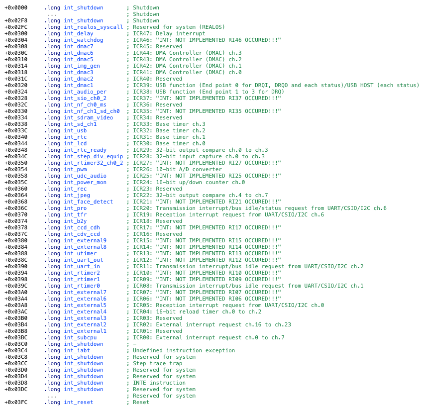
The interrupt vector table can be found by accessing the TBR (Table Base Register): It usually occurs in the vector reset handler at the very beginning of the firmware. Handler addresses in the table are stored in the reverse order of the formula , so that the reset vector at the end of the table is offset . I found most of the interrupts from the FR manual and suggested that Leica Maestro has a similar layout. Then he took each handler and tried to find a string or any other hint revealing the purpose of the interruption. As a result, I made the following list: Many interrupts are quite expected, such as AUDIO / SDIO / VIDEO / JPEG / RAW, but try to determine the most mysterious of them? I'm talking about interruption . It seems that the camera supports some kind of console mode UART CLI.
 LDI:32 #int_table, R0

 MOV R0, TBR
TBR + (0x3FC - 4 × inum)0x3FCint_uart_inSystem calls
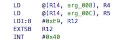
Like almost any OS, Softline REALOS uses system calls. In assembly language, they look like this: The
actual address of the system call handler is calculated as follows. Let's start by looking for an interrupt handler
INT #0x40. As described above, it is (0x3FC - 4 × inum) = (0x3FC - 4 × 0x40) = 0x2FC = int_realos_syscalleasy to find a reference in the handler to the bottom of the system call table with 16-bit words. The specific entry in this table is calculated by the formula
syscall_table_bottom + (num * 2): [syscall_table_bottom + (-23 * 2)] = [syscall_table_bottom - 0x2E] = [0x1012EA] = 0xE68This does not look like an address, because the actual address of the system call handler is calculated as
syscall_table_bottom + offset. The whole process is shown in the diagram. All system calls and their functionality are listed in the Softline REALOS / FR Core Guide.so I was able to restore all the implemented handlers in the table and further improve the IDB.
Of course, you can make the code even more beautiful by defining the types of system calls in IDA.
I wrote a Python script to automatically search for these system calls and so on.
Tasks
In the system call,
sta_tskI noticed that as a parameter, not the main function is passed, but pid. That means it's time to look for a large array of task handles. And it makes sense to start from the very sta_tsk.ROM: 102180 sys_sta_tsk: ROM: 102180 ST RP, @ -R15 ROM: 102182 LDUB @ (R14, 0x4F), R3 ROM: 102184 LDI: 32 # word_100B80, R14
At the very beginning we see some links. I had to tinker with the data types, but in the end the parts came together:
ROM: 100B80 word_100B80: .word 0xF; number of tasks
ROM: 100B82 .word 0x1C; task descriptor size
ROM: 100B84 .long 0x82A09F5C; task 1 descriptor
ROM: 100B88 .long 0x1000D
ROM: 100B8C .long 0
ROM: 100B90 .long 0x40000000
ROM: 100B94 .long sub_1A7DB2; task main
ROM: 100B98 .long 0x8286EEC0
ROM: 100B9C .long 0
ROM: 100BA0 .long 0x82A09F88; task 2 descriptor
ROM: 100BA4 .long 0x20010
ROM: 100BA8 .long 0
ROM: 100BAC .long 0x40000000
ROM: 100BB0 .long sub_1A6BD2; task main
ROM: 100BB4 .long 0x8287EEC0
ROM: 100BB8 .long 0
...
and so on. Only 15 tasks. It was a matter of time to look into each main function, to determine the name and purpose of the task (except for the last). Here is the complete list:
- SubCPU
This task appears to be responsible for capturing operations such as exposure, sighting on the screen, etc. - KeyManager
Most likely, this task is associated with hardware buttons. - GuiManager
Quite a big task, which implements the UI state machine and interface drawing. - DebugManager
Yes, there is something to debug. Om-Nom-nom. - FileManager
This task is all about file operations. - FamManager
I would say that the task is responsible for files and memory, because it depends on the tasks of the file manager and the memory manager. - MemoryManager
No surprises: memory operations, pool management, etc. - ImageManager
This task manages the encoding / decoding processes and other image processing processes. - UsbManager
The current task is to handle USB communications, which includes MassStorage, PTP and its own Leica protocol. - IOManager
It looks like this task manages storage devices such as SD cards and CF cards (what? What else CF? Maybe from model 213). - Systemmanager
Various tasks like general system operations, power management, etc. - SettingsManager
Handles camera status and settings. - MonitorManager
Monitors camera status changes and informs other tasks. - PeripheralManager
This task controls the GPS, brightness and some other sensors. - Unknown
Unfortunately, for her, I did not find anything substantial.
It is interesting to note that after the main array there is another outstanding descriptor. And the task function is simply branching itself. This handle is referenced at the end of the function , which is responsible for creating other tasks and setting up the firmware. So this is most likely the task of inactivity of the system.
ROM:100D28 dword_100D28: .long 0x82A0A1F0

ROM:100D2C .long 0x21

ROM:100D30 .long 0

ROM:100D34 .long 0x80000000

ROM:100D38 .long tid16_task

ROM:100D3C .long 0x8285EEC0

ROM:100D40 .long 0
ROM:101494 sub_101494:
ROM:101494 BRA sub_101494 ; CODE XREF: sub_101494startModules and Messages
In addition to tasks, you can define some logical objects, such as IO and peripheral modules. Modules are presented as a group of message handlers in one of the tasks.
The IO group seems to include:
- IO Manager
- Subprocessor
- USB manager
- USB PTP
- Leica USB protocol
- USB Mass Storage
- Button Manager
- Debug manager
- Lens manager
And in the peripheral group:
- Peripherals Manager
- Light sensor
- LEDs
- Speaker
- Tilt angle sensor
- Cap Recognition
- GPS module
- 3DAxis module
The messaging system itself uses standard SOFTUNE structures:
struct RealOS_MsgPayload
{
  uint32_t msgID;   // +0x0
  uint32_t data[];  // +0x4
}
struct RealOS_Message
{
  uint32_t            os_reserved1; // +0x0
  uint32_t            os_reserved2; // +0x4
  uint32_t            to;           // +0x8
  uint32_t            from;         // +0xC
  RealOS_MsgPayload*  payload;      // +0x10
}
As expected, IPC also has several message groups. Since many messages are processed in tasks and modules, I was able to restore only some of these groups:
0x1101xxxx - global system messages:
             0x11010002 = SYS_UPDATE_BOOTLOADER or
             0x11010005 = SYS_ERASE_SETTINGS
0x1102xxxx - messages related to image capture:
             0x11020001 = CMD_CAP_CAPTURE or
             0x11020008 = IMAGE_STATUS_CHANGED
0x1104xxxx - messages about events related to playback:
             0x11040002 = PLY_DISABLE_PLAY_MODE or
             0x11040004 = PLY_IMAGE_READY
0x1108xxxx - various messages for debugging PTP, etc .:
             0x11080002 = DBG_CHANGE_LEVEL or
             0x11080012 = DBG_WRITE_ROM_DUMP_SD
0x2201xxxx - USB PTP messages
             0x22010108 = changing camera settings or
             0x22010118 = DebugObject Request
0x2202xxxx - a rather large group of SUBCPU messages:
             0x22020002 = E_SUBCPU_REQUEST_M_EXPOSURE_REQUEST
             0x22020015 = E_IO_SUBCPU_COMMAND_CLEANING_SENSOR
0x2203xxxx - some other debug messages:
             0x22030001 = debug line command
0x2204xxxx - various IO messages:
             0x2204000C = Enable / Disable Mass Storage or
             0x22040012 = reboot device
0x330000xx is another message group for the UI:
             0x33000001 = keystroke
             0x33000007 = lens connection
0x440000xx - there is little information here, but it looks like image processing
             0x44000013 = E_IMG_CMD_CHANGE_PINFO
0x55xxxxxx - FAM message groups:
             0x558800xx = FAM file manager or
             0x558888xx = first group of FAM menu settings
0x6602xxxx - similar to LED control messages, for example:
             0x66020001 - LED switching from X Hz
             0x66020002 = LED continuous on
0x6604xxxx - beeper management:
             0x66040001 = beeper setting
             0x66040007 = squeak about the filled map
0x6611xxxx - memory related debug messages
0x6622xxxx - memory-related message handling messages
0x6660xxxx - some other messages related to the memory:
             0x66600006 = HISTOGRAM
             0x66600011 = RAWCOMP
0x771100xx and 0x77AA00xx - messages related to switching camera modes
Unfortunately, many other messages remain unknown.
GUI
In the firmware file, let's look at the following sections: CTRL_SYS-11 , IMG-LOKI-212 , IMG-DSP-212 , IMG-FPGA-212 and IMG-LENSDATA-212 .
What surprised me was the complete lack of GUI resources. But they must be somewhere and, most likely, embedded in IMG-LOKI-212 .
One of my usual approaches to reverse firmware development is to restore all possible cross-references. Not only in the code, but also in the data section. Then I look at them, trying to find some patterns or links to known parts of the code.
Leica firmware is no exception. There are many similar data sequences with addresses to other data sequences that go further, and so on. Going up the link hierarchy, I finally saw a familiar function.
For example, I found a data structure without any references:
g_data = { ... }She was addressed by another structure:
g_data_struct1 = { ... , &g_data }Which in turn is addressed by another structure:
g_data_struct2 = { &g_data, ... }This data structure has a link from the code, and it is passed as a parameter to another function:
func1()
╰ func2(..., &g_data_struct2, ...)
However,
func1()it is not called directly from another function, but is stored in some array:g_func_list1[] = { ..., func1(), ... }Having looked above, I found a call in the code
g_func_list1:func3() {
g_func_list1[x]
}Again, this function is stored in an array:
g_func_list2[] = { ..., func3(), ... }Some other code refers to the array itself:
func4() {
    g_func_list2[x]
}
Fortunately, this time the function is called from another function, and so on
gui_MADE_ApplicationRun.gui_Statemachine_DoStateChange()
╰ gui_MADE_ApplicationRun()
╰ func5()
╰ func4()Some lines indicate that the GUI subsystem is called “MADE”, and page transitions are processed using
MADE_GetSysTriwhatever that means. The GUI state machine is basically implemented in a function gui_Statemachine_DoStateChange. After collecting information about the GUI, a general picture emerged: As you can see, the main function for GUI resources is
gui_CopyImageDesc(although this is not a real name). She has the following arguments:gui_CopyImageDesc(
uint32_t dstAddress; // R4 - destination address
UIDescType type; // R5 - description type
UITarget target; // R6 - rendering target
uint32_t descAddress; // R7 - description address
uint8_t always0; // (SP + 0x0) - always 0
uint8_t index1; // (SP + 0x4) - index 1
uint8_t index2; // (SP + 0x8) - index 2
uint16_t x_offset; // (SP + 0xC) - x offset
uint16_t y_offset; // (SP + 0x10) - y offset
uint16_t unknown2; // (SP + 0x14) -
uint32_t language1; // (SP + 0x18) - language id 1
uint32_t language2; // (SP + 0x1C) - language id 2
uint32_t funcAddress; // (SP + 0x20) - function address
)There are four types of resource descriptions:
struct UIDescType0Header         struct UIDescType1Header         struct UIDescType2                struct UIDescType3
{                                {                                {                                 {
    uint32_t    address;             uint32_t    address;             uint32_t    reg;                  uint16_t    x_offset;
    uint16_t    entries;             uint16_t    entries;             uint32_t    address;              uint16_t    y_offset;
    uint16_t    unknown;             uint16_t    unknown;             uint16_t    unknown1;             uint32_t    address;
}                                }                                    uint16_t    unknown2;         }
                                                                      uint16_t    unknown3;
struct UIDescType0Entry          struct UIDescType1Entry              uint16_t    tableoff;
{                                {                                }
    uint16_t    x_offset;            uint16_t    x_offset;
    uint16_t    y_offset;            uint16_t    y_offset;
    uint32_t    address;             uint32_t    address;
}                                    uint16_t    objects;
                                     uint16_t    total_w;
                                     uint16_t    total_h;
                                     uint16_t    unknown;
                                 }
The first type has a header with a link to an array of records. Each entry has the coordinates and address of the pixel data. The current type seems to describe state-dependent elements, such as icons, which can be grayed out or disappear from the UI.
The second type also starts with a header and is used for localization, description of lines or blocks of text.
The third type describes character maps for different languages.
The latter type is responsible for all other static resources, such as images, backgrounds, etc.
Now, take a look at the data for images themselves. The first six bytes look like a small header, followed by some kind of repeating pattern, where every second byte is either or . It is logical to assume that and
+0x00: 00 08 00 14 00 01 A2 FF 0A 04 05 FF 0C 04 03 FF

+0x10: 0D 04 03 FF 0E 04 02 FF 0E 04 02 FF 04 04 06 FF

+0x20: 04 04 02 FF 04 04 06 FF 04 04 02 FF 04 04 06 FF

+0x30: 04 04 02 FF 04 04 06 FF 04 04 02 FF 04 04 06 FF

+0x40: 04 04 02 FF 04 04 06 FF 04 04 02 FF 04 04 06 FF

+0x50: 04 04 02 FF 04 04 06 FF 04 04 02 FF 0E 04 02 FF

+0x60: 0E 04 02 FF 0D 04 03 FF 0D 04 03 FF 0C 04 04 FF

+0x70: 04 04 0C FF 04 04 0C FF 04 04 0C FF 04 04 0C FF

+0x80: 04 04 0C FF 04 04 0C FF 04 04 0C FF 04 04 0C FF

+0x90: 04 04 0D FF 02 04 2D FF 00 06 00 14 00 01 79 FF0xFF0x040x00080x0014 - width and height in the view with direct byte order (big endian). At the end of this dump, we see the beginning of another sequence 00 06 00 14 00 01. Most likely, this is the next resource (as evidenced by a link to it). Thus, the size of the actual image data is 146 bytes. But the image size should be 0x8 * 0x14 = 0xA0 = 160. It is clear that the data is not pure pixels and not even an 8-bit LUT, because it is 14 bytes smaller. What then? Probably some kind of compression. Looking at this hex dump, it's hard to believe that some complicated scheme is being used. Leica's GUI is not very colorful, so in my experience it’s best to use the LUT table. In this case, the UI resources will completely repeat the LUT indexes like
03 03 03orА1 А1 А1. Usually the compressor tries to get rid of data duplication, replacing them with a link. These index arrays are ideal for compression even with a simple method like RLE [data][number]. Simple command to write data(value) numbertimes. With all this in mind, I assumed that there was most likely a simple image with two colors LUT (
0xFFand 0x04) in front of us , and the byte before the color was the number of pixels to draw. “And then you wrote another tool,” you think. But no, I took a pen and paper and began to fill the cells. It's funny that I still have that picture.
Somewhere along the way, I realized that 160 pixels is not enough for this image, so 0x8 and 0x14 need to be multiplied by two. The third word 0x0001 indicates whether the image is an ASCII character, so the final ImageAsset structure is as follows:
struct ImageAsset
{
    uint16_t    width;        // ширина/2 (big endian)
    uint16_t    height;       // высота/2 (big endian)
    uint16_t    ascii;        // 1, если символ ASCII
    struct      image_data {
        uint8_t number;       // количество пикселей для рендеринга
        uint8_t color;        // индекс цвета пикселя в LUT
    } data[];
}
But one part is still missing: LUT.
It was not so difficult to find, because many links and structures were already manually restored, so I slowly scrolled through the data sections, looking for an array of 256 elements from 16-bit or 32-bit values, until I came across this: Again, thanks In my work with Blackmagic Design, I immediately recognized the YUV pixels (for example, all values with 8080 digits). I'm not stupid to draw the whole user interface again on paper, so yes, I wrote another tool - M240UITool . In addition to resetting all image resources from a firmware file to BMP / PNG, this tool can create IDC scripts in IDA to determine all UI resources.
 .long 0x7008080, 0x72D8080, 0x73C8080, 0x75A8080, 0x79B8080, 0x71DFF6B, 0x7BE8080, 0x7FF8080

 .long 0x77BBD27, 0x75B60E7, 0x7835F4A, 0x7D3089F, 0x7018080, 0x7028080, 0x7038080, 0x7048080

 .long 0x7058080, 0x7068080, 0x7078080, 0x7088080, 0x7098080, 0x70A8080, 0x70B8080, 0x70C8080

 .long 0x70D8080, 0x70E8080, 0x70F8080, 0x7108080, 0x7118080, 0x7128080, 0x7952B15, 0x7138080

 .long 0x7148080, 0x7158080, 0x7168080, 0x7178080, 0x7188080, 0x7198080, 0x71A8080, 0x71C8080

 .long 0x71D8080, 0x71E8080, 0x71F8080, 0x7338080, 0x7208080, 0x7218080, 0x7228080, 0x7238080

 .long 0x7248080, 0x7248080, 0x7268080, 0x7278080, 0x7288080, 0x7298080, 0x72A8080, 0x72B8080

 .long 0x72C8080, 0x75E8080, 0x7608080, 0x7628080, 0x7648080, 0x7678080, 0x7688080, 0x7698080

 .long 0x76B8080, 0x76E8080, 0x7708080, 0x7728080, 0x7758080, 0x7778080, 0x7798080, 0x77C8080

 .long 0x77E8080, 0x7818080, 0x7838080, 0x7868080, 0x7888080, 0x78B8080, 0x78D8080, 0x7908080

 .long 0x7928080, 0x7958080, 0x7978080, 0x7998080, 0x79C8080, 0x79D8080, 0x7668080, 0x79E8080

 .long 0x7A18080, 0x7A28080, 0x7A38080, 0x7A68080, 0x7A78080, 0x7A88080, 0x7AB8080, 0x7AC8080

 .long 0x7AD8080, 0x7B08080, 0x7B28080, 0x7B58080, 0x7B88080, 0x7B98080, 0x7BC8080, 0x7CC8080

 .long 0x7AB3BBB, 0x7E10094, 0x7E4556E, 0x4008080, 0x2922D17, 0x7B2AB00, 0x7C2A262, 0x71DFF6B

 .long 0x768D4A2, 0x769D4EA, 0x7BD88AE, 0x705997B, 0x70BB377, 0x711CC73, 0x717E66F, 0x7238866

 .long 0x729A262, 0x72FBB5E, 0x735D55A, 0x7417751, 0x747914D, 0x74DAA48, 0x753C444, 0x75F663B

 .long 0x76B9933, 0x7998080, 0x771B32F, 0x77D5526, 0x7836F22, 0x789881E, 0x78FA21A, 0x7159095

 .long 0x71AAA91, 0x720C38D, 0x726DD88, 0x7506F6A, 0x7568866, 0x75CA262, 0x762BB5E, 0x76E5E55

 .long 0x7747751, 0x77A914D, 0x780AA48, 0x78C4D3F, 0x792663B, 0x7988037, 0x79E9933, 0x7AA3C2A

 .long 0x7B05526, 0x7B66F22, 0x7BC881E, 0x72488AE, 0x72AA1AA, 0x72FBBA6, 0x735D4A2, 0x7427799

 .long 0x7489095, 0x74DAA91, 0x753C38D, 0x77E556E, 0x7836F6A, 0x7898866, 0x78FA262, 0x79C4459

 .long 0x7A15E55, 0x7A77751, 0x7AD914D, 0x7BF4D3F, 0x7CC8080, 0x7C5663B, 0x7CB8037, 0x7337FC8

 .long 0x73999C4, 0x73FB2C0, 0x745CCBB, 0x7757799, 0x74C54FF, 0x77B9095, 0x780AA91, 0x7AB3C72

 .long 0x7B1556E, 0x7B66F6A, 0x7BC8866, 0x74277E1, 0x74890DD, 0x74EAAD9, 0x754C3D5, 0x76066CC

 .long 0x7667FC8, 0x76C99C4, 0x772B2C0, 0x77E55B7, 0x7846EB3, 0x78A88AE, 0x790A1AA, 0x7526EFB

 .long 0x75787F7, 0x75DA1F3, 0x763BAEE, 0x76F5DE6, 0x77577E1, 0x77B90DD, 0x781AAD9, 0x78D4CD0

 .long 0x79366CC, 0x79F99C4, 0x7E10094, 0x7CF44A1, 0x7DB7799, 0x7E71A90, 0x7ED338C, 0x7FF8080

 .long 0x7328080, 0x7DC8080, 0x7C88080, 0x7508080, 0x775CD2C, 0x76944EA, 0x7808080, 0x71A61FF

 .long 0x7244D40, 0x7242C15, 0xFFF8080, 0xF338080, 0xF668080, 0xF998080, 0xFCC8080, 0xF008080

 .long 0xF4C54FF, 0xFAB3BBB, 0xFE10094, 0xFE4556E, 0xF952B15, 0xFDA7751, 0xFB2AB00, 0xFC2A262

 .long 0xF1DFF6B, 0xF68D4A2, 0xF69D4EA, 0xFBD88AE, 0xA922D17, 0xC6E4130, 0xE286963, 0x74C55FF

 .long 0x768D536, 0x7FF8080, 0x7FF8080, 0x7FF8080, 0x2922D17, 0x46E4130, 0x6286963, 0x8080
Leica M (typ 240) UI Tool v1.0
Usage: ./M240UITool [-a address] [-i imagebase] [-s script] [-d dump] [-f folder] [-l LUT] [-rbv] FIRMWARE.BIN
This tool will help you to find UI resources in firmware.
Use following arguments:
-a Specify address of the gui_CopyImageDesc function (ex. 0x2F95E0)
-i Specify firmware imagebase
-s Specify IDC file name
-c Specify container file name
-d Specify dump image format
png - PNG format
bmp - BMP (ARGB) format
-f Specify folder for dumped images
-l Specify LUT for images (filename of address)
-b Specify number of bytes to display in verbose mode
-r Try to recover string characters
-v Be verboseWe already know that from the function that one UI page creates, it is called several times
gui_CopyImageDesc. I thought it would be great to make the UI resource browser and define all page rendering functions. The option -c is for this purpose - it creates a special container for viewing resources. And who said that the UI resource browser might not look unusual?
Being interactive (translucent buttons on the screenshot), this tool allows you not only to scroll through the EVF / LCD menu pages, but also to view the rendering steps within one page.
Unfortunately, the source code of this masterpiece is lost somewhere, but the header files are still in the M240UITool code, so you can technically recreate it from scratch.
Debug menu
What line are we looking for in the first place during reverse engineering? In my opinion, this word
debugand its derivatives. The firmware had a lot of interesting lines, but these are special: It seems that you can enter debug mode using some kind of key combination. All of these lines are called from a single giant function that implements a button-scanning state machine. Here’s what it looks like in IDA:
$ strings ./IMG_LOKI-212_1.1.0.2.bin | grep "Debug Mode"

GUI: State: %d! Scanning for Debug Mode successful

GUI: Scanning for Debug Mode: State: %d, Ignore long DEL

GUI: Scanning for Debug Mode: State: %d

GUI: Scanning for Debug Mode: State: %d, Ignore long DEL

GUI: Scanning for Debug Mode: State: %d

GUI: Scanning for Debug Mode: State: %d, Ignore long DEL

GUI: Scanning for Debug Mode: State: %d

GUI: Scanning for Debug Mode: State: %d, Ignore long DEL

GUI: Scanning for Debug Mode: State: %d

GUI: Scanning for Debug Mode: State: %d, Ignore long DEL

GUI: Scanning for Debug Mode: State: %d

...

GUI: ScanningForDebugWithKeyAndJoyStick(): g_GUI_CheckForDebugWithKeyAndJoyStick = %dScanningForDebugWithKeyAndJoyStickI will not lie, it took some time to understand how the hardware buttons are processed in the firmware, and then to restore the enumerated types for the buttons and the joystick. But when I got the combination, I found out with distress that she was not doing anything. It probably works only from a specific GUI page. A couple of evenings of manual tracing of the GUI state machine - and the problem was solved, and the Reset menu page was also found.
Finally, welcome to debug mode.
I thought a lot, whether to announce this combination, but decided to abstain. I respect the hard work that Leica does when releasing its unique devices, and I don’t want to be responsible for the fact that their service centers fill in broken carcasses of cameras as a result of some thoughtless curiosity.
But still, I will provide some enumerated types in order to simplify reverse engineering for those who are ready to follow this path.
enum ControlActionType {
    kControlAction_Idle,        // 0
    kControlAction_Push,        // 1
    kControlAction_Release,     // 2
    kControlAction_LongPush     // 3
};
enum ControlBtnType {
    kControlBtn_LV,             // 0
    kControlBtn_PLAY,           // 1
    kControlBtn_DEL,            // 2
    kControlBtn_ISO,            // 3
    kControlBtn_MENU,           // 4
    kControlBtn_SET             // 5
};
enum ControlJoystickType {
    kControlJoy_INFO,           // 0
    kControlJoy_Up,             // 1
    kControlJoy_Down,           // 2
    kControlJoy_Left,           // 3
    kControlJoy_Right           // 4
};
PTP
Thinking over the USB task, I defined three modes (which is also confirmed in the debug menu):
- PTP
- MSC (Mass Storage Class)
- Leica Custom
PTP is most interesting because it is well documented and allows you to control the camera.
It is quite easy to find PTP handlers in the firmware, because there are a lot of calls from this code. All PTP calls are divided into three groups: Legacy , Leica Extended (LE) and Production .
Debug messages helped to set titles for almost the entire code.
Legacy: Leica Extented: Production:
0x1001 - GetDeviceInfo 0x9001 - Set Camera Settings 0x9100 - Open Production Session
0x1002 - OpenSession 0x9002 - Get Camera Settings 0x9101 - Close Production Session
0x1003 - CloseSession 0x9003 - Get Lens Parameter 0x9102 - UpdateFirmware
0x1004 - Get Storage ID 0x9004 - Release Stage 0x9103 - Open OSD Session
0x1005 - Get Storage Info 0x9005 - Open LE Session 0x9104 - Close OSD Session
0x1006 - GetNumObjects 0x9006 - Close LE Session 0x9105 - Get OSD Data
0x1007 - GetObjectHandles 0x9007 - RequestObjectTransferReady 0x9106 - GetFirmwareStruct
0x1008 - GetObjectInfo 0x9008 - GetGeoTackingData 0x910B - GetDebugMenu
0x1009 - GetObject 0x900A - Open Debug Session 0x910C - SetDebugMenu
0x100A - Get Thumb 0x900B - Close Debug Session 0x910D - ODIN Message
0x100B - Delete Object 0x900C - Get Debug Buffer 0x910E - GetDebugObjectHandles
0x100E - Initiate Capture 0x900D - Debug Command String 0x910F - GetDebugObject
0x1014 - GetDevicePropDesc 0x900E - Get Debug Route 0x9110 - DeleteDebugObject
0x1015 - GetDevicePropV 0x900F - SetIPTCData 0x9111 - GetDebugObjectInfo
0x101C - Initiate Open Capture 0x9010 - GetIPTCData 0x9112 - WriteDebugObject
0x9020 - Get3DAxisData 0x9113 - CreateDebugObject
0x9030 - OpenLiveViewSession 0x9114 - Calibrate 3Daxis
0x9031 - CloseLiveViewSession 0x9115 - Magnetic calibration
0x9033 - Unknown 0x9116 - Get Viewfinder Data The implementation of the PTP interface itself seems standard, but some commands have limitations, which I intentionally omit here.
In any case, all of the above is quite fascinating. You might think, "Let's just connect the camera via USB and start probing using libptp." That's right.
Only damn ...
The Leica M240 does not have a USB port.
Handle port
Leica offers some accessories for this camera, but there is one particularly interesting. This is a multi-function handle Leica M (14495) . It replaces the lower metal part of the body, provides a built-in GPS and several connectors like USB, a SCA flash terminal, DIN / ISO-X and a power jack.
And again you will say: “Great, now just buy it, attach it to the camera, connect the camera via USB and start probing with the help of libptp”. That's right.
Only damn ...
It costs almost $ 900.
This is almost nine hundred reasons to create your own adapter. However, just in case, I set up eBay notifications for this accessory.
Connector
The connector on the camera looks like this:
I tried to find it on the Internet, but seriously, how would you describe it in Google?
A little desperate, I started thinking about some crazy things, like sticking foil or needles to a rubber eraser. But once at work in Blackmagic Design, looking at the printed circuit board of the camera, I noticed that one connector had a very familiar shape. The next day I brought my Leica M240 to work - and yes, it looked similar, just much longer with more contact pads.
It remains to ask the part number from our component manager, and then find it in the Samtec catalog: ERM8-013-05.0-L-DV-TR .
We also asked Samtec representatives if a sample could be obtained, and they kindly agreed.
A bit of work with a soldering iron, cardboard and electrical tape - and my own plug is ready (sample 2013).
Five years later, in 2018, I decided to personally ask Samtec to send another sample. I wanted to do something better.
ERCD-013-05.00-TTR-TTR-1-D
Again, a lot of work with a soldering iron, swearing, cutting the wire, swearing, again working with a soldering iron to make a new, more attractive option:
Pinout
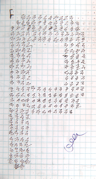
In the connector 26 contacts: 13 on each side. Even before soldering my part, I probed the camera connector with a multimeter and a logic analyzer. By the way, you need to put a magnet on the bottom cover sensor so that the camera thinks that the cover is in place.
Earth (camera off, no battery)
I always start from the ground because it is safe and very easy to find.
Thus, we have eight ground lines (dark gray).
Potential (camera on)
When the camera is on, you can measure the potential at each contact and get an idea of the logic and power levels.
alexhude.github.io/assets/2019/2019-01-24-hacking-leica-m240/probe2_potential.png
The numbers on pins 8-9 and 11-13 are too high for logical contacts, so I defined them as power (red).
Resistance (camera off, no battery)
It is also useful to measure resistance. In some cases, it helps to identify entrances and group some lines.
Connected outputs (camera off, no battery)
Then I decided to check all external pads on the camera body to check if they are connected to the service port.
The flash sync switch was directly connected to line 10.
Logic analyzer (camera turned on) The
data for each line was recorded in the following sequence: turn on, the camera should be in LV mode, take a picture, start video recording.
Two lines show the transfer of some data: 01 and 21.
01 - 115200, transmission of 8 bits, 1 stop bit, parity bit, LSB first.
Every 500 ms, it sends some kind of counter
C3 3C 02 81 00 01 00 82, C3 3C 02 81 01 01 00 83, C3 3C 02 81 02 01 00 80... 21 - 115200, 8-bit transmission, 1 stop bit, no parity bit, first LSB.
It sends the SH7216 bootloader log (“Leica Camera AG” in the screenshot above).
Let's mark them dark blue. It is rather sad that the Maestro log does not give out even with the maximum debugging settings in the Debug menu.
At these contacts, the resistance is about 310kOhm.
I do not know why, but I assumed that other data lines may have similar resistance or will be closed. Therefore, I defined ~ 300kOhm, ~ 200kOhm and ~ 100kOm lines as data lines as well (shades of blue in the figure).
In general, the following picture was drawn.
12 candidates for data lines. But how to check them? After a brief conversation with the hardware experts about the electrical protection of integrated circuits, I started poking at the contacts through a 4kOhm resistor, reducing the current to a level that should not burn the inputs.
UART
I made another assumption that the line RX should be next to the TX. Lines 02, 03 and 20 look like good candidates, because both have 3.3 V voltage like TX.
Initially, I tried to explore these lines using the Bus Pirate. Unfortunately, the result was pretty messy. Then I took the SiLabs based cables as more reliable and non-conflicting with macOS.
First, I connected the TX cable to pin 20 and started dialing
helpafter the bootloader. As expected, after a short delay, the camera repeated the characters. Contacts 02 and 03 were the next UART candidates. Unfortunately, there were no signs that these lines are tapped.
On the diagram, the famous UARTs are indicated by a darker shade of green.
USB
It all started with a cut USB cable in half with a header in the middle and 4kOhm resistors for sensing. Signal integrity of a differential pair? Nope, then it didn't really bother me. :)
Then I sounded at home several household devices with USB to get an idea of what the communications on this port looked like.
Canon
camera Blackmagic pocket camcorder
Canon
camcorder JVC camcorder
Keyring
KidiZoom camera
They are all a little different, but the initial state of D-D + is low. Well, we will know, and now we will check that we have:
- 22 - unlikely, because D- D + are a differential pair and should be pretty close;
- 04/05 - unlikely, because they have different resistance;
- 14/15 - unlikely, because they have different resistance;
- 15/16 - perhaps because they are close and have similar resistance.
So I connected the USB D-D + to the pins 15/16 and connected to the iMac ...
On the USB PTP screen, but the camera did not appear on the host. I tried to configure different options on the layout of the electronic scheme, but nothing worked. Beagle showed a lot of damaged packages and other errors. In the end, I gave up and went back to reverse engineering the firmware.
This is the final pinout, USB is marked in dark green.
Who would have thought that a few years later, that eBay notification would come to me and I would rather cheaply buy the desired accessory.
Finally, I can check my assumptions about PTP. But at first it was very curious how the USB PHY looks inside the gadget.
Inside was the hub SMSC 2512bRight on the road from the grip connector to the Mini USB connector. The chip works in default mode, because there is no EEPROM or SCL / SDA pins. The first downstream port is routed to the socket of the camera body, but the second is not connected to anything.
Probably, I missed something, but for me such a decision does not make much sense. The technical data sheet says that the chip has “fully integrated USB leads, and also has resistors for boosting and lowering the voltage.” Perhaps Leica’s engineers decided not to implement their own USB PHY, but used the one in the hub, which is well tested and works out of the box. In fact, I can not blame them, because before I tried to do this, and it turned out to be a daunting task. Maybe this is a feature to protect against forgery, who knows.
In any case, if you understand USB PHY and are ready to help, do not hesitate to write to me: it should be possible to work through the USB port without this branded accessory :)
PTP again
As I said, it's time to play around with the Leica PTP extension.
Fortunately, I found a pretty cool C ++ library instead of libptp - this is libEasyPTP . It also didn't take long to write a tool based on this library: I already knew some limitations in the Leica PTP interface.
And although M240PTPTool is pretty buggy, it is quite suitable for the role of proof of concept ( program code ).
There are only two requests for PTP: GetDebugBuffer (0x900C) and DebugCommandString (0x900D) . By the way, in order for the modules to fill in the debug log, you need to set the Debug Level in the menu as “Debug” or “Debug RAW”.
There are several options in the M240PTPTool interface:
- exit - close the tool;
- flush - drain the debug buffer from the camera:
M240> flush

I:[00:11:468]|01| DATE/TIME CORRECTED by 5921 sec

D:[00:12:079]|00| Send message from TID 0 to TID 1 over MBX 3 - length: 4 - MesgID: 0x22020103

D:[00:12:179]|00| Send message from TID 0 to TID 1 over MBX 3 - length: 4 - MesgID: 0x22020103

D:[00:12:282]|11| Message received from TID 0 for TID 1 over MBX 3

D:[00:12:283]|11| Message received from TID 0 for TID 1 over MBX 3

D:[00:12:301]|00| Send message from TID 0 to TID 1 over MBX 3 - length: 4 - MesgID: 0x22020103

D:[00:12:402]|00| Send message from TID 0 to TID 1 over MBX 3 - length: 4 - MesgID: 0x22020103

D:[00:12:502]|00| Send message from TID 0 to TID 1 over MBX 3 - length: 4 - MesgID: 0x22020103

...
Any other text is sent to the camera as a debug command. For example, it
helpdisplays all possible commands with arguments: The
complete list is quite large, but see, you can send direct messages to Softune for any task! What would be so interesting to send there ...
Another popular line, which is often sought in the firmware - . Let's see if we have one.
Apparently, you can dump the firmware to the SD card. The link to the line “Dumping files to card” makes it easy to find the code responsible for it. It is located in the giant System Task block (pid 11, as we already know) and is called by a message with no arguments.
Type in M240PTPTool , press Enter and look at the screen.M240> help
********* debug command description ********
exposure request
Description: requests a release from Sub CPU
Parameter 1: Exposure Time TV
still request
Description: simulates the -still request- command flow of Sub CPU
Parameter: no
...
send Message;[Parameter1];[Parameter2];[Parameter2];...;...
Description: Sending Message to Task
Parameter 1: Receiver Task ID
Parameter 2: Command ID
Parameter 3: Command Data[0] (32 Bit)
Parameter 4: Command Data[1] (32 Bit)
Parameter 5: .
Parameter 6: .
use maximum 10 Parameter
...dump$ strings IMG_LOKI-212_1.1.0.2.bin | rg -i dump
GUI: HEX DUMP: Address: %x, Length: %d
HSK: DBG_WRITE_ROM_DUMP_SD: File was properly opened, but it seems to be empty.
ROM_DUMP
HSK: DBG_WRITE_ROM_DUMP_SD: Flushing Dump to ROM. Size %d
SD:\ROM_DUMP.bin
HSK: DBG_WRITE_ROM_DUMP_SD Command received!
ROM_DUMP.bin
HSK: DUMP failed, no cards inserted!
HSK: DUMP FlashROM to SD card.
HSK: DUMP FlashROM to CF card.
Dumping files to card0x11080006send Message;11;0x11080006Then remove the SD card and check what is on it.
Here it is, a complete dump, including the firmware.
This opens up endless possibilities. For example, you can make a tiny device with an MCU, USB host support and buttons to launch complex message sequences ...
And then we had a second child. :)
Epilogue
If you do not want to break the device, there is usually a way to examine it without opening the case or soldering the wires to the circuit board. Below are my tips if you're interested:
- find all public information about the device: technical specifications, data on components, photos of entrails, videos from the factory ;)
- if you have firmware, rummage through it and look for tips on external outputs;
- always google different magic and weird sequences of bytes, which you will find in the firmware files;
- measure GND / potential / resistance for all unknown contacts exposed to the outside;
- probe these contacts with a logic analyzer;
- always remember about the safety measures associated with electronics;
- Try to exclude contacts that you do not need (land, food);
- if you cannot recognize the signal by analog form, try searching Google for the most popular (USB / UART / SPI / I2C / 1Wire);
- If you have an idea about the nature of the signal, try checking for similar consumer electronics;
- think
three tofive times before sending data to the device; - and of course do not hesitate to ask for advice.
github.com/alexhude
Good luck to you hacks!