August 9, 2012 at 01:22
Allegro Cadence 16.5

To develop electronics, you need at least knowledge of circuitry, knowledge of the modern electronic base of components, the ability to work in one of the CAD programs and breed boards in accordance with the requirements of EMC. And if you have not yet decided which CAD system you will mainly work with, then this article is for you.
Currently, there are three professional CAD environments for electronics: Altium Designer, Allegro Cadence and Mentor Graphics PADS. Any semi-professional types like Proteus, Eagle, etc., should not even be considered, since they are not allowed to be done at the level of amateur radio and any complicated things. There are various archaic, specialized ones, such as Microwave, Uniboard and others, but they should not be considered either because of their low popularity and, as a result, the lack of support.
In this article I want to give an overview and talk a bit about how to work in Allegro Cadence, since I use this environment myself for such reasons:
- First off, Cadence's capabilities are quite impressive. To list everything will only take a separate article, but I will talk about something below.
- Secondly, Cadence is not very demanding on the system, it will work fine even on very weak computers like 1GHz, 512 RAM. If your computer does not have 2 cores, then in fact you have no choice but Cadence, because during development, often, if not always, you have to simultaneously keep several software packages open at once, in my case SolidWorks and Cadence, if I had started, for example, Altium, my computer would have just gone out of smoke.
- Thirdly, there are no such bugs as in Altium (I don’t know about Pads). Cadence, of course, has some inconvenient things, I must say here they have their own shell, completely built on scripts and controlled from the command line, it may seem inconvenient to many, but there aren’t such critical errors like Altium when converting files to gerberas and generally a fairly stable environment in this regard.
So what is Allegro Cadence? This is a package of programs and utilities that are well connected with each other. Each program is responsible for its own area and is launched separately. There are quite a lot of them and there is a need for a separate article to talk about any of them, so I will list and briefly tell only about those that an ordinary electronic engineer needs to just know what to start working with.
Design Entry CIS
This program is for designing a circuit diagram, its simulation, drawing circuits, etc. Those. here you create or paste components, bind footprint to them, indicate the rules that will be checked at the end to exclude errors, rooms, etc. In general, in Design Entry CIS your whole project can be, including documentation, but for a start this is all redundant information, so I’ll briefly tell you what and how to do it.
File-> New-> Project
All created. Go to the page of the PAGE1 schematic diagram and click Place Part, then Add Library and select the necessary libraries. You can create your own component libraries and you even need to, and you need to add them to the project as well.
Picture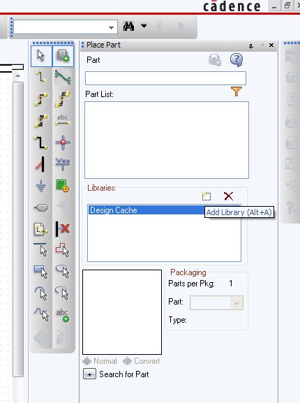
Ok, add the Discrete and MicroController library of discrete elements. Suppose we want to make a circuit containing a pair of resistors, capacitors and an STM32 microcontroller. To do this, select the Discrete library and search above in the Part List “CAP POL” and “RESISTOR”, i.e. polar capacitor and resistor. We insert them into the circuit and then we look for STM32 microcontrollers in the MicroController library. But bad luck, they are not there. What do we do? Build a chassis from scratch?
No, there is an easier option, right-click on an empty place in the diagram and select Place Database Part from the menu and in the opened tab click on Internet Component Assistant
Picture
In the built-in browser window, click on Active Parts with the opamp icon. Next, in the window that opens, we see a bunch of settings, but we touch nothing, and drive into the Part Number: “STM32” line.
Picture
Next, select the controller we need or close to it (so that we can finish it a bit), indicate which library to embed, indicate if there is a footprint, etc. If you do not know what to indicate, then click on Place Part constantly.
To attach footprint to a component, you need to go into its properties by double-clicking on the component and find the corresponding graph. The name of the footprint is the name of its file, and the footprints themselves are in the directory .. \ Cadence \ SPB_16.5 \ share \ pcb \ pcb_lib \ symbols you can’t change it, but if you find where, it’s better not to, Cadence really doesn’t like it when it they indicate something wrong. On the other hand, if he doesn’t like something, he will tell you for sure.
Just want to talk about the files that are in the folder .. \ symbols.
* .dra - files of our components, in other words our footprint
* .bsm - mechanical holes
* .pad - files of
pads * .psm - files of padstack, in general, should be in the same place where * .dra
In order to make a board you need to know more one thing is how to make a netlist so that you can breed a board. To do this, you need to go to the project page, select it and click on Create netlist, there are 1500 settings, but I believe that you will figure it out. And don’t worry, if Cadence is dissatisfied with something, then he will not allow you to ruin the circuit and will send you an error, and he does it often. Be sure you will still love him, even if you first hate him. C'est la vie.
Package designer
If you have generated an error when creating netlist Cadence, then most likely you are missing a footprint somewhere. There are two ways to fix this, the first is to exclude the component from the physical model, and the second to add, and if not, create the footprint component. To do this, we need the Package Designer program. The environment here is the same as in the PCB Editor design program, so almost everything is the same here, both management and many functions.
It opens files of the * .dra type, so that you don’t have to worry much, go to the symbol directory in the .. \ pcb_lib \ symbols folder and open some file with the * .dra extension. You will see a component consisting of heaps of layers. Now a little about how to live in this space at all, because if you try to cry and do something sane, you will be surprised how everything is inconvenient here, but this is at first glance ... in general, at the second and third too, as I said to Cadence, you still hate it, but it's nothing then you laugh and even fall in love with him, so don’t say goodbye, it’s forever. Seriously.
Picture
So, the management here is a bit unusual. Holding the middle mouse button, you can move the window, for zoom you need to twist the mouse wheel. Everything here is done something like this: clicking on an object-> right mouse button-> command-> execution. You need to practice, it’s not immediately clear how and why, you will understand later. Much is being done from the command line, there is a separate discussion about this.
On the right we see the control panel, which consists of three tabs: Options, Visiability, Find
Picture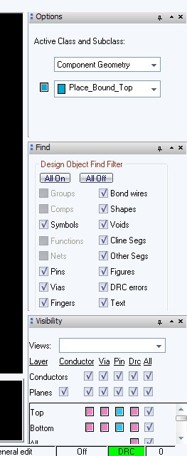
Options - the classes of layers we are going to work with are listed there, only a few are sure to know.
Find - here we note with which specific elements we will work with, and if it is easier which ones we will choose. Suppose if I want to select only pins, and not touch the pipes, then I must tick Pins.
Visiability - here we mark which elements will be visible to us and which are hidden so as not to interfere. There are not all layers, but only the main ones.
All that you can learn on the panel yourself, I’ll tell you only the main things here.
Menu Display-> Color / Visiability - here you configure the colors of the elements and their visibility on the diagram.
Setup-> Design Parameters Menu- An important menu that sets up the project. Grids - grid, with what step you will move the elements. Text - default text setting.
The Setup-> Areas-> Part Height menu is a very important option, if you want to transfer the board to a 3D model, it sets the height of the component by binding to the Place_Bound_Top / Bottom layer.
Shape menu - here is the management of shapes. Shapes are anything from a polygon to a component body.
Menu Layout-> Pins - insert pins.
In general, this is all for this program, I repeat that here it is the same as in the PCB Editor, many options are even the same. But we will consider it later, because To create a component, we need to be able to create our own pads, and for this we need the following utility.
Pad designer
As you may have guessed, this utility creates the pads that you need in order to assign them to components in the Package Designer. There are a lot of settings here and it is difficult to find what is not here, starting from the arbitrary pad shape to drilling holes using a plasma or laser, in general, all this is important for production. First, open some * .pad in the .. \ symbols folder, so you can see how and what to enter.
PCB Editor
Finally, we moved on to the most important program. It allows you to arrange your components and wiring them according to the wiring diagram. Here is the same as in Package Designer, but only more. There is no point in talking about this program in detail, because only about it you can write a dozen articles, there are a lot of tricks, subtleties, pitfalls, etc. I will list only important menus so that you don’t look for them during development.
Manufacture menu - everything about preparation for board production. Transfer to gerberas, the legend of drills, the scheme of layers and more.
Cross section (Xsection) - physical layers are assigned there. Their number, thickness, material, order. This can be obtained from the board manufacturer.
Constraint manager- this is a whole subroutine, it sets the rules for wiring and clearances, for example, you can make rats not show one of the net-s.
In general, the rest is more or less understood by trial and error. Just for clarity and as an example I will show a piece of a divorced board:

In general, everything was a brief overview, just to understand how and what is arranged here, of course, it’s not enough to just read the article and you need to install Cadence and make a board to understand what ideology is there. This is not just an ordinary program for Windows, if you sit on it then you won’t get off. Perhaps at first a lot of things will seem uncomfortable to you, but after understanding the details you will understand that everything is so even right.
And three more points. When wiring the board, when you work with polygons you need to enter this commandset etchedit_ignore_dynamic_shapes otherwise it would be unrealistic to breed something, the polygons will interfere with the tracks and you will die dragging them. Does it surprise you that without a single team that is not spelled out anywhere it’s unrealistic to breed a normal board? Well, that's it, Cadence, you will first despise the sadists who made it, but then everything will change and besides Cadence -a you will no longer need another CAD system.
The second point is this. It’s not necessary to create footprints manually, as There are many programs that generate them for you. The most famous are LP_Wizard and PCB Library Editor, they are paid. But there is one more, and in my opinion a very good and kind of free Footprint maker, you can download it here.
The third point is the need to use the command line. It is practically impossible to do without it, but in principle, one pair of commands is enough for a start, as I said above, and the second command is the introduction of coordinates. For example, you need to draw a 10x10 polygon, switching the grid is unrealistic each time, and sometimes it doesn’t help, so do this, select the polygon in shapes and enter in the line: “x 0 y 0”, the pointer will move to the origin and enter again : “X 10 y 10” and you get a 10 by 10 square. You can also use the move, delete, and other commands. For example, “move x 120 y 100” moves the object to the specified point. It’s very convenient to use the Show Element tool, it will give you all the info about the object and you can easily move the object 1 mm to the right using the command line, simply adding the coordinates and driving it into a line.
Update 08.19.12
I learned here that there are sensible lessons on creating footprints, they are really in English, but that's okay, in principle, everything is more or less clear.
Manual footprint tutorial