SamsPcbGuide Part 6: Tracing Signal Lines. Loss and Crosstalk Models
I really hoped to publish with the mood "Russia - in the semifinals", but a little was not enough. Although for me always the character was higher than the result, and the character I saw. Thanks guys. We continue to improve in what we can. They are in football, we are in the design of printed circuit boards. Let's go, the sixth part. It examines the effect of line losses on the signal edge duration, provides a model of crosstalk, and provides recommendations for reducing them.
In the previousThe article showed that line inconsistency leads to reflections and signal distortion. All matching methods involve ensuring that the impedances of the load and / or source are equal to the wave impedance of the signal line. From this it follows that if the load impedance is unstable and depends on some parameter, it is impossible to ensure exact matching. For example, the input cascade of logic elements is always characterized by an equivalent input capacitance (usually units of picofarad). The voltage at the input capacitor V during transients, and therefore its impedance

depend on time. The reflections arising in this case are expressed in the slowing down of the front duration by the time τ ≈ 2.2 ∙ Z 0 C (by analogy with the RC circuit). If the duration of the source front t R is small compared to τ, then it is the process of charging the capacitor that will determine the duration of the front at the far end of the line.
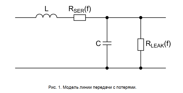
In a real signal line, the signal front slows down not only with an increase in the capacitive load on it, but also due to losses caused by ohmic losses and leakage losses in the dielectric. In fig. 1 shows a lossy line model where the series resistance

models ohmic losses (including skin effect), and resistance

dielectric (here tg (δ) is the loss tangent, the characteristic of the dielectric material). The increase in losses with increasing frequency leads to the fact that the high-frequency components of the signal are attenuated more significantly, which leads to a slowdown of the signal front. Eric Bogatin in [1] gives a formula for estimating the front duration at the output of a signal line with losses of length L and a dielectric with permeability ε and loss tangent tan (δ):

Further, from the condition Δt R = t R OUT -t R IN <0.1 ∙ t R IN, we can derive an estimated criterion for the necessity of taking into account the effects associated with losses in the signal line.
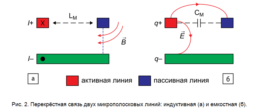
Another source of loss is cross-coupling with adjacent conductors (eng.), Which leads to distortion of the signal in the active line (due to losses in the near field) and induced crosstalk in the passive line. The effect arises due to two physical principles - electrical (capacitive) coupling and magnetic (inductive) coupling. In fig. Figure 2 shows the determining parameters of the cross-coupling — the mutual inductance L M and the mutual capacitance C M , which depend primarily on the geometry and parameters of the materials.
Shown in fig. 3 An equivalent cross-talk circuitry can be used for calculations and simulations. The number N of such consecutive links should be the greater, the higher the electric line length TD and the required spectral band of the BW model:

The capacitance C L and the inductance L L of the links can be calculated by the formulas:

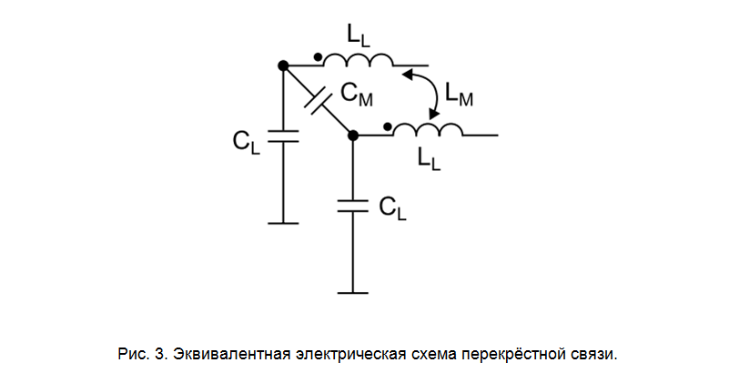
The main difficulty in modeling the equivalent cross-coupling scheme is to calculate the values of L M and C M per one link. For some cases, there are estimated analytical relationships [2], in the general case, specialized software tools based on numerical methods are used to solve this problem.

The equivalent circuit is electrically short (for a time delay of which TD <1/5 ∙ t R of the passive line is performed, see Fig. 5, where the sources of electrical energy are determined by the formulas:

The circuit is simplified and is applicable only for estimating the amplitude of crosstalk. However, for this scheme, analytical relationships are derived that show the main dependencies, which are also true for more complex cases:

The above theory has, for simplicity, considered an example of two conductors. However, it is important to understand that a typical situation for digital printed circuit boards is when several signal lines synchronously change their state. Since crosstalk from several active lines is added up, in this case the amount of interference can become critical, leading to incorrect functioning of the system. In this case, specialized software is used for numerical simulation, but the fundamental principles for reducing the amount of crosstalk remain the same as the above recommendation.
[1] Bogatin E. “Signal and power integrity - simplified”, 2nd ed., Pearson, 2010
[2] “Mutual Inductance and Capacitance Algorithm”, rev. 01.8.2
[3] Adamczyk B. “EMC Crosstalk between PCB Traces”, West Michigan EMC Chapter Meeting, 2013 This
article was first published in Components and Technology 2018, No. 4. The publication on Habr has been agreed with the editors of the magazine.
In the previousThe article showed that line inconsistency leads to reflections and signal distortion. All matching methods involve ensuring that the impedances of the load and / or source are equal to the wave impedance of the signal line. From this it follows that if the load impedance is unstable and depends on some parameter, it is impossible to ensure exact matching. For example, the input cascade of logic elements is always characterized by an equivalent input capacitance (usually units of picofarad). The voltage at the input capacitor V during transients, and therefore its impedance
depend on time. The reflections arising in this case are expressed in the slowing down of the front duration by the time τ ≈ 2.2 ∙ Z 0 C (by analogy with the RC circuit). If the duration of the source front t R is small compared to τ, then it is the process of charging the capacitor that will determine the duration of the front at the far end of the line.
In a real signal line, the signal front slows down not only with an increase in the capacitive load on it, but also due to losses caused by ohmic losses and leakage losses in the dielectric. In fig. 1 shows a lossy line model where the series resistance
models ohmic losses (including skin effect), and resistance
dielectric (here tg (δ) is the loss tangent, the characteristic of the dielectric material). The increase in losses with increasing frequency leads to the fact that the high-frequency components of the signal are attenuated more significantly, which leads to a slowdown of the signal front. Eric Bogatin in [1] gives a formula for estimating the front duration at the output of a signal line with losses of length L and a dielectric with permeability ε and loss tangent tan (δ):
Further, from the condition Δt R = t R OUT -t R IN <0.1 ∙ t R IN, we can derive an estimated criterion for the necessity of taking into account the effects associated with losses in the signal line.
As can be seen from this recommendation, in most PCB applications, you can use the lossless signal line model, where R LEAK = ∞ and R SER = 0.R.1.
For a signal line whose length L corresponds to the criterion L [cm] <5 / (tg (δ) ∙ √ε) ∙ t R [ns], the influence of losses on the signal edge duration can be ignored. For the insulator FR4, this condition takes the form L [cm] <125 ∙ t R [ns].
Another source of loss is cross-coupling with adjacent conductors (eng.), Which leads to distortion of the signal in the active line (due to losses in the near field) and induced crosstalk in the passive line. The effect arises due to two physical principles - electrical (capacitive) coupling and magnetic (inductive) coupling. In fig. Figure 2 shows the determining parameters of the cross-coupling — the mutual inductance L M and the mutual capacitance C M , which depend primarily on the geometry and parameters of the materials.
Shown in fig. 3 An equivalent cross-talk circuitry can be used for calculations and simulations. The number N of such consecutive links should be the greater, the higher the electric line length TD and the required spectral band of the BW model:
The capacitance C L and the inductance L L of the links can be calculated by the formulas:
The main difficulty in modeling the equivalent cross-coupling scheme is to calculate the values of L M and C M per one link. For some cases, there are estimated analytical relationships [2], in the general case, specialized software tools based on numerical methods are used to solve this problem.
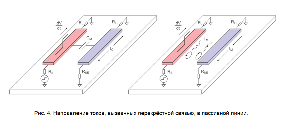
Electrical and magnetic coupling leads to energy loss and distortion of the signal in the active line and the appearance of the signal in the passive line. Capacitive I C and inductive I M coupling currents (Fig. 4) are unidirectional towards the source (near-end) and oppositely directed towards the load (far-end):R.2.
The mutual inductance and mutual capacitance decrease with increasing distance between the conductors and with decreasing distance between the conductor and the reference layer. In addition, the presence of cutouts in the reference layer leads to a significant increase in mutual inductance.
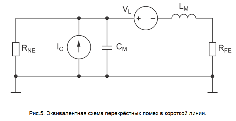
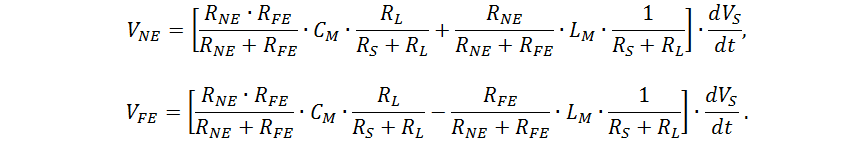
The equivalent circuit is electrically short (for a time delay of which TD <1/5 ∙ t R of the passive line is performed, see Fig. 5, where the sources of electrical energy are determined by the formulas:
The circuit is simplified and is applicable only for estimating the amplitude of crosstalk. However, for this scheme, analytical relationships are derived that show the main dependencies, which are also true for more complex cases:
In fig. Figure 6 shows the waveforms of measuring crosstalk between two 50-ohm microstrip lines on an experimental board in two cases: w ~ 2.5 mm, s ~ 0.6 mm, h = 1.39 mm and w ~ 0.6 mm, s ~ 1.9 mm, h = 0.3 mm. The length of the parallel sections of the tracks is about 30 cm. It is worth paying attention to the fact that the duration of the signal edges on the active line significantly exceeds the typical values for high-speed digital printed circuit boards. The amount of interference in fig. 5 should not be considered as characteristic, these waveforms are primarily a visual representation of the influence on the amount of interference of the duration of the signal front, the distance between the conductors and the proximity of the reference layer.R.3.
Crosstalk Reduction Methods:
- Increasing the duration of the signal fronts in the active line (eng. Aggressor, active line).
- Decrease in a parallel section of lines.
- Increased distance between conductors. There are recommendations for the minimum distance between the edges of the printed tracks s ~ 6 ∙ h or s ~ 3 ∙ w, where h is the distance to the support layer, w is the width of the track.
- Reducing the distance between the conductor and the reference layer.
- Selection of resistances at the ends of active and passive (English victim, quiet line) lines.
- The use of shielding conductors (English guard trace) shorted to the support layer at the ends and, if possible, along the length (of the order of three vias per length t R ∙ v).
- The use of embedded microstrip (English embedded microstrip) or strip lines, for which, due to the symmetry of the dielectric, V FE ≈ 0.
The above theory has, for simplicity, considered an example of two conductors. However, it is important to understand that a typical situation for digital printed circuit boards is when several signal lines synchronously change their state. Since crosstalk from several active lines is added up, in this case the amount of interference can become critical, leading to incorrect functioning of the system. In this case, specialized software is used for numerical simulation, but the fundamental principles for reducing the amount of crosstalk remain the same as the above recommendation.
Literature.
[1] Bogatin E. “Signal and power integrity - simplified”, 2nd ed., Pearson, 2010
[2] “Mutual Inductance and Capacitance Algorithm”, rev. 01.8.2
[3] Adamczyk B. “EMC Crosstalk between PCB Traces”, West Michigan EMC Chapter Meeting, 2013 This
article was first published in Components and Technology 2018, No. 4. The publication on Habr has been agreed with the editors of the magazine.