Connecting a color LCD with a touch screen to the microcontroller
Good afternoon, habr. Today I would like to share some experience regarding the connection of color LCD-indicators to the microcontroller. This topic has already been raised on the hub ( http://habrahabr.ru/post/139384/ ), so this post can be considered as an addition to the one already written by my esteemed colleagues.

In the post referenced at the beginning, LCD indicators connected via the SPI interface are discussed. This connection method is simple, but not the only one. Many indicators have “on board” only a simplified controller that does not have memory for storing the image, and therefore requires continuous updating of the image. Such indicators are used everywhere in electronic gadgets, and for their functioning a special LCD controller is needed, which is built into the microcontroller. An example of such an indicator is MI0350CT-3 manufactured by Multi-Inno Technology. This is a fairly typical representative of color LCDs, having a resolution of 320 * 240 and a resistive sensor.
So, we have some problem. Let each pixel be represented in memory by a 32-bit value (only 24 of them are used, but the data is aligned on 4-byte boundaries). In total, under one video page we need 320 * 240 * 4 = 307200 bytes = 300 KB of RAM. Not every microcontroller has such an amount of memory. Therefore, as a rule, an external memory is required for the LCD to work, and therefore an external memory controller on a microcontroller chip.
In fairness, it should be noted that the requirements for memory size can be reduced if you use not 24-bit per pixel, but a smaller color depth, but, on the other hand, we may want to place several video pages in the system memory in order to be able to quickly switch between them . We will return to this topic later.
As an example, consider connecting an LCD to an LPC2478 microcontroller. This is a slightly outdated representative of the NXP microcontrollers (on the ARM7 core, and not on the modern Cortex M3), but for our purposes this is not essential. This microcontroller contains everything you need: an external memory controller (with the ability to connect both SRAM and SDRAM), and an LCD controller with the possibility of very flexible settings.
For experiments, I used the SK-MLPC2478 board, which, in addition to the LPC2478 microcontroller, has a K6R4008V1D-TI10 static memory chip (CMOS SRAM) with a capacity of 512Kx8 bit. The aforementioned MI0350CT-3 indicator is connected to the board.
There is another pitfall: this indicator requires a source with an output current of 20 mA at a voltage of about 20 V. ma If the load is not connected, then the converter operates in the mode of stabilization of the output voltage (U o = 20 V). The converter circuit is shown in Fig. 1. The principle of operation and calculation of the boost converter will not be considered here, those interested in this topic can refer to the documentation for the MC34063A chip.

Fig. 1. The voltage converter.
Let us briefly consider the connection and operation of this type of LCD. The LCD uses 24 signals for color information, a CLK signal for pixel synchronization, HSINK and VSINC signals for horizontal and vertical pulses. In addition, the indicator has an SPI interface for setting auxiliary registers, a #RESET signal and a DEN (data enable) signal. The SPI interface in this case is not intended to transmit an image to the display controller, but to configure auxiliary registers. These registers allow you to select the mode of operation of the indicator, adjust the brightness, contrast and other parameters. However, the indicator control registers are set to the desired state by default, and if we are not going to change them, the SPI signals can simply be ignored. The #RESET signal can simply be set to inactive (single) state.
So, the main signals necessary for this type of indicator to work are: data signals that carry information about the current pixel color in RGB format, CLK clock signal, vertical and horizontal synchronization signals, and also a data resolution signal. Consider the timing charts.

Fig. 2. Timing diagram of data transmission in LCD.
In fig. 2 shows the most “large-scale” data transfer timing diagram depicting data transmission of one image line. Transmission occurs on the edge of the CLK signal, and is accompanied by a high DEN data resolution signal. The transmission takes place in RGB format, while the Data0 - Data7 bits correspond to blue, Data8 - Data15 bits to green, Data16-Data23 to red.
Before transmitting the string data and after transmitting the data, “empty”, non-information-carrying pulses CLK are inserted. The line feed is preceded by a horizontal synchronization pulse HSYNC (LCD_LP).
The clock frequency of the indicator is 6.4 MHz (it can be reduced, but then the flicker of the frames becomes noticeable).
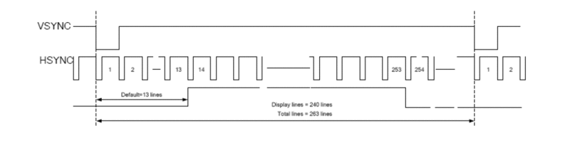
Fig. 3. Timing diagram of frame transmission in LCD The
timing diagram of transmission of a full frame in LCD is shown in Fig. 3. The transmission of the frame begins with 13 “empty” lines, then 240 lines with the image, followed by “empty” lines again. Frame transmission begins with a vertical sync pulse.
We also connect a resistive sensor to the microcontroller. A description of this connection will be given below.
I will not give a complete diagram of connecting the indicator to the microcontroller, due to its obviousness, I will only give a table of correspondence between the indicator pins and the controller pins.
Table 1. Correspondence of LCD signals and controller outputs
We assemble the device layout (Fig. 4-6):

Fig. 4. Board layout device

Fig. 5. The device layout (partially assembled)
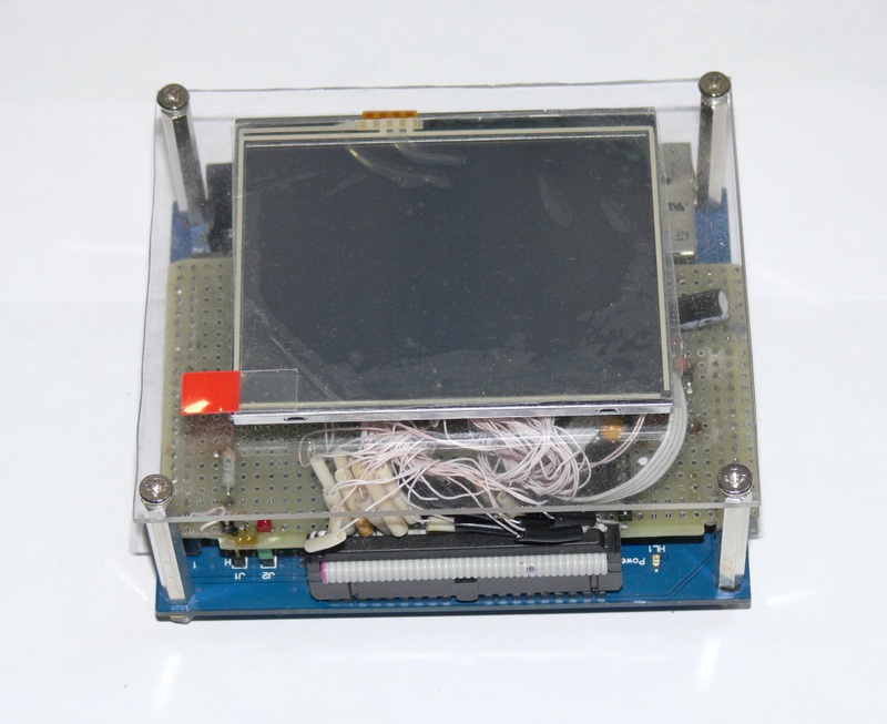
Fig. 6. The layout of the device assembly
Now that everything is connected, you can start writing code. The first thing to do is configure and test external SRAM memory:
SRAM test:
It should be understood that the performance of external memory is an important factor. In fact, the data stream in our case is Fclk * N, where Fclk is the clock frequency of the indicator, N is the number of bytes in memory allocated for 1 pixel. Total we get 6.4 * 10 ^ 6 * 4 = 25.6 MB / s. For memory with an 8-bit interface, this means a maximum allowable access time of 39 ns. Memory performance requirements can be reduced by using memory with a 16 or 32-bit interface and / or reducing the color depth used.
We configure the LCD in, setting the signal duration in accordance with the indicator documentation:
Now we write a test picture in ROM and copy it to RAM:

Fig. 7. Test picture. The picture is
written as an unsigned int [240] [320] array and copied to the base address of the external memory (0x80000000).
The operation of the LCD support mechanism built into the microcontroller consists in the fact that the data is read from the RAM by the DMA controller and fed to the LCD controller, where the cursor image is superimposed and the data is fed to the LCD input. Also, the LCD controller can provide palette support for modes from 1 to 8 bits per pixel. The palette is implemented in the microcontroller as 256 16-bit registers and, thus, provides the mapping of 8-bit color to 16-bit (5 bits / color + 1 bit of total intensity).
The cursor has a separate palette of two 32-bit registers; it provides a monochrome image of the cursor in a 24-bit color space. The cursor can be 64x64 pixels or 32x32 pixels in size, and contains both the cursor image itself and the image inversion mask.
Now you can run the test program and look at the result.
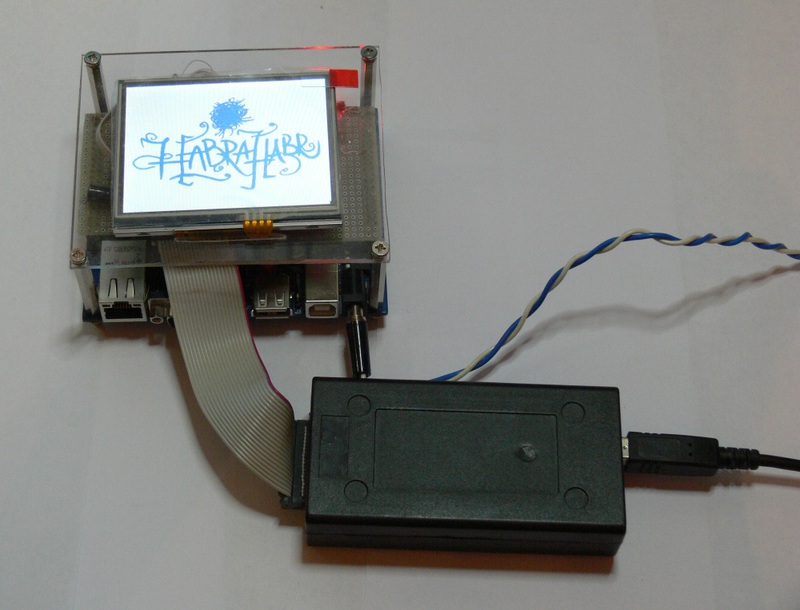
Fig. 8. The result of the work.
The principle of operation of a resistive sensor is widely known (those who are not familiar with it can see it, for example, here http://ru.wikipedia.org/wiki/Touch screen ). Therefore, we proceed immediately to the description of connecting the sensor to the microcontroller. This device uses a four-wire sensor. The connection diagram is shown in fig. 9.
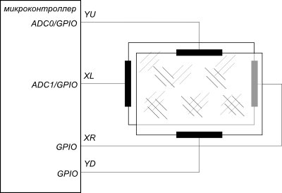
Fig. 9. The connection diagram of the resistive sensor to the microcontroller.
The idea underlying this connection is as follows. Each pin of the microcontroller can be in one of the following states: output with a logical 0, output with a log. 1, an input (i.e., in fact, an unconnected output), and an input pulled up to the supply voltage through a resistor. The YU and XL pins can also serve as ADC inputs.
The whole procedure for determining the coordinates of pressing can be conditionally divided into three phases. In the first phase, the conclusions to which the sensor is connected are in the following state: (Fig. 10).
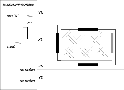
Fig. 10. Determination of the coordinates of pressing. Phase 1.
When the sensor films are closed, a log signal is received at the input of the microcontroller. 0, and the program proceeds to phase 2, determining the x-coordinate of pressing (Fig. 11). This is followed by phase 3, determination of the y-coordinate. (fig. 12).

Fig. 11. Determination of the x-coordinate of pressing.
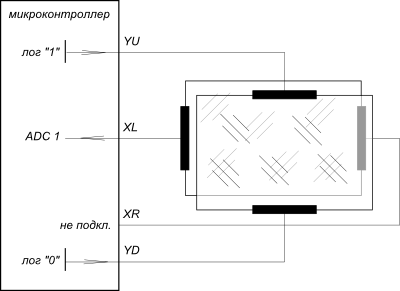
Fig. 12. Determination of the y-coordinate of pressing.
Of course, the algorithm for calculating the coordinates of pressing must include the suppression of the bounce of “contacts” (sensor films).
With a single measurement, the accuracy of determining the coordinates will be too low, the noise of the measurements will lead to the fact that the cursor will fluctuate strongly in the vicinity of the point of contact. Therefore, it is highly desirable to use some kind of filtering algorithm, for example a median filter ( http://en.wikipedia.org/wiki/Median_filter ).
After receiving the result in the ADC codes, it is recalculated into the coordinates of the screen using the usual linear transformations (ax + b), where the coefficients a and b must be found by calibrating the sensor and stored in the non-volatile memory of the controller. In fig. 13. An example calibration screen is provided.

Fig. 13. Calibration screen.
Fig. 14. Calibration screen on the LCD.
It is also possible to connect the touch screen using an external controller, for example, XPT2046.
The full source code for the sample program can be downloaded from here: https://bitbucket.org/arktur04/lcd-demo (IAR development environment).
Links to the documentation mentioned in the post:
1. Display Multi-Inno MI0350CT-3 http://www.displayfuture.com/engineering/specs/TFT/MI0350CT-3.pdf
2. Pulse voltage converter MC34063A http: //www.fairchildsemi .com / ds / MC / MC33063A.pdf
3.LPC2478 microcontroller http://www.ru.nxp.com/products/microcontrollers/arm7/lpc2400/LPC2478.html
4. XPT2046 resistive sensor controller http: //www.dzsc .com / uploadfile / company / 785710 / 20111014212155973.pdf
In the post referenced at the beginning, LCD indicators connected via the SPI interface are discussed. This connection method is simple, but not the only one. Many indicators have “on board” only a simplified controller that does not have memory for storing the image, and therefore requires continuous updating of the image. Such indicators are used everywhere in electronic gadgets, and for their functioning a special LCD controller is needed, which is built into the microcontroller. An example of such an indicator is MI0350CT-3 manufactured by Multi-Inno Technology. This is a fairly typical representative of color LCDs, having a resolution of 320 * 240 and a resistive sensor.
So, we have some problem. Let each pixel be represented in memory by a 32-bit value (only 24 of them are used, but the data is aligned on 4-byte boundaries). In total, under one video page we need 320 * 240 * 4 = 307200 bytes = 300 KB of RAM. Not every microcontroller has such an amount of memory. Therefore, as a rule, an external memory is required for the LCD to work, and therefore an external memory controller on a microcontroller chip.
In fairness, it should be noted that the requirements for memory size can be reduced if you use not 24-bit per pixel, but a smaller color depth, but, on the other hand, we may want to place several video pages in the system memory in order to be able to quickly switch between them . We will return to this topic later.
As an example, consider connecting an LCD to an LPC2478 microcontroller. This is a slightly outdated representative of the NXP microcontrollers (on the ARM7 core, and not on the modern Cortex M3), but for our purposes this is not essential. This microcontroller contains everything you need: an external memory controller (with the ability to connect both SRAM and SDRAM), and an LCD controller with the possibility of very flexible settings.
For experiments, I used the SK-MLPC2478 board, which, in addition to the LPC2478 microcontroller, has a K6R4008V1D-TI10 static memory chip (CMOS SRAM) with a capacity of 512Kx8 bit. The aforementioned MI0350CT-3 indicator is connected to the board.
There is another pitfall: this indicator requires a source with an output current of 20 mA at a voltage of about 20 V. ma If the load is not connected, then the converter operates in the mode of stabilization of the output voltage (U o = 20 V). The converter circuit is shown in Fig. 1. The principle of operation and calculation of the boost converter will not be considered here, those interested in this topic can refer to the documentation for the MC34063A chip.
Fig. 1. The voltage converter.
Let us briefly consider the connection and operation of this type of LCD. The LCD uses 24 signals for color information, a CLK signal for pixel synchronization, HSINK and VSINC signals for horizontal and vertical pulses. In addition, the indicator has an SPI interface for setting auxiliary registers, a #RESET signal and a DEN (data enable) signal. The SPI interface in this case is not intended to transmit an image to the display controller, but to configure auxiliary registers. These registers allow you to select the mode of operation of the indicator, adjust the brightness, contrast and other parameters. However, the indicator control registers are set to the desired state by default, and if we are not going to change them, the SPI signals can simply be ignored. The #RESET signal can simply be set to inactive (single) state.
So, the main signals necessary for this type of indicator to work are: data signals that carry information about the current pixel color in RGB format, CLK clock signal, vertical and horizontal synchronization signals, and also a data resolution signal. Consider the timing charts.
Fig. 2. Timing diagram of data transmission in LCD.
In fig. 2 shows the most “large-scale” data transfer timing diagram depicting data transmission of one image line. Transmission occurs on the edge of the CLK signal, and is accompanied by a high DEN data resolution signal. The transmission takes place in RGB format, while the Data0 - Data7 bits correspond to blue, Data8 - Data15 bits to green, Data16-Data23 to red.
Before transmitting the string data and after transmitting the data, “empty”, non-information-carrying pulses CLK are inserted. The line feed is preceded by a horizontal synchronization pulse HSYNC (LCD_LP).
The clock frequency of the indicator is 6.4 MHz (it can be reduced, but then the flicker of the frames becomes noticeable).
Fig. 3. Timing diagram of frame transmission in LCD The
timing diagram of transmission of a full frame in LCD is shown in Fig. 3. The transmission of the frame begins with 13 “empty” lines, then 240 lines with the image, followed by “empty” lines again. Frame transmission begins with a vertical sync pulse.
We also connect a resistive sensor to the microcontroller. A description of this connection will be given below.
I will not give a complete diagram of connecting the indicator to the microcontroller, due to its obviousness, I will only give a table of correspondence between the indicator pins and the controller pins.
Table 1. Correspondence of LCD signals and controller outputs
| Signal | SK-MLPC2478 (connector X6) | LCD pin | Microcontroller port | Note |
| GND | 1 | 53, 54 | land | |
| + 5V | 2 | - | not used | |
| DATA6 | 3 | 18 | data | |
| +3.3 V | 4 | 41, 42 | nutrition | |
| LCD CLK IN | 5 | - | not used | |
| DATA 7 | 6 | 19 | data | |
| DATA 19 | 7 | 31 | data | |
| DATA 18 | 8 | thirty | data | |
| DATA 22 | 9 | 34 | data | |
| DATA 23 | 10 | 35 | data | |
| DATA 20 | eleven | 32 | data | |
| DATA 21 | 12 | 33 | data | |
| DATA 14 | thirteen | 26 | data | |
| DATA 15 | 14 | 27 | data | |
| DATA 12 | fifteen | 24 | data | |
| DATA 13 | 16 | 25 | data | |
| DATA 11 | 17 | 23 | data | |
| DATA 10 | 18 | 22 | data | |
| DATA 1 | 19 | thirteen | data | |
| DATA 0 | 20 | 12 | data | |
| DATA 9 | 21 | 21 | data | |
| DATA 8 | 22 | 20 | data | |
| DATA 17 | 23 | 29th | data | |
| DATA 16 | 24 | 28 | data | |
| LCD LE | 25 | - | not used | |
| LCD PWR | 26 | - | not used | |
| LCD FP | 27 | 37 | Vertical sync | |
| LCD CLK | 28 | 38 | Indicator Clocking | |
| LCD LP | 29th | 36 | Horizontal sync | |
| LCD ENAB | thirty | 52 | Data resolution | |
| DATA 5 | 31 | 17 | data | |
| DATA 4 | 32 | 16 | data | |
| DATA 3 | 33 | fifteen | data | |
| DATA 2 | 34 | 14 | data | |
| SPENA | 35 | 43 | P0.20 | SPI interface, serial port data enable |
| - | 36 | - | Not used | |
| #RESET | 37 | 6 | P0.19 | discharge |
| - | 38 | - | Not used | |
| SPCK | 39 | 49 | P0.17 | SPI interface, serial port clock |
| SPDA | 40 | fifty | P0.18 | SPI interface, serial data |
| Yu | Connector X7.15 | 8 | AD0 / P0.23 | Resistive Sensor |
| Xr | Connector X7.13 | 9 | AD1 / P0.24 | Resistive Sensor |
| Yd | Connector X7.10 | 10 | P0.26 | Resistive Sensor |
| XL | Connector X7.12 | eleven | P0.25 | Resistive Sensor |
We assemble the device layout (Fig. 4-6):
Fig. 4. Board layout device
Fig. 5. The device layout (partially assembled)
Fig. 6. The layout of the device assembly
Now that everything is connected, you can start writing code. The first thing to do is configure and test external SRAM memory:
// Init SDRAM controller
  // Enable EMC clock
  PCONP_bit.PCEMC    = 1;
  EMCSTATICWAITRD0   = 0x00000001;
  EMCSTATICWAITPG0   = 0x00000000;
  EMCSTATICWAITWR0   = 0x00000000;
  EMCSTATICWAITTURN0 = 0x00000000;
  EMCCONTROL      = 1;         // enable EMC
SRAM test:
char SRAM_Test(void)
{
// 32 bits access
  for (Int32U i = 0; i < 0x80000; i+=sizeof(Int32U))
  {
    *(Int32U*)(((Int32U)SRAM_BASE_ADDR)+i) = i;
  }
  for (Int32U i = 0; i < 0x80000; i+=sizeof(Int32U))
  {
    if (*(Int32U*)(((Int32U)SRAM_BASE_ADDR)+i) != i)
    {
      printf("Verification error on address : 0x%x\n",(Int32U)SRAM_BASE_ADDR+i);
      return(FALSE);
    }
  }
  return TRUE;
}
It should be understood that the performance of external memory is an important factor. In fact, the data stream in our case is Fclk * N, where Fclk is the clock frequency of the indicator, N is the number of bytes in memory allocated for 1 pixel. Total we get 6.4 * 10 ^ 6 * 4 = 25.6 MB / s. For memory with an 8-bit interface, this means a maximum allowable access time of 39 ns. Memory performance requirements can be reduced by using memory with a 16 or 32-bit interface and / or reducing the color depth used.
We configure the LCD in, setting the signal duration in accordance with the indicator documentation:
// Init GLCD cotroller
  PCONP_bit.PCLCD = 1;      // enable LCD controller clock
  CRSR_CTRL_bit.CrsrOn = 0; // Disable cursor
  LCD_CTRL_bit.LcdEn = 0;   // disable GLCD controller
  LCD_CTRL_bit.LcdBpp= 5;  //2bpp // 24 bpp
  LCD_CTRL_bit.LcdTFT= 1;   // TFT panel
  LCD_CTRL_bit.LcdDual=0;   // single panel
  LCD_CTRL_bit.BGR   = 0;   // normal output
  LCD_CTRL_bit.BEBO  = 0;   // little endian byte order
  LCD_CTRL_bit.BEPO  = 0;   // little endian pix order
  LCD_CTRL_bit.LcdPwr= 0;   // disable power
  // init pixel clock
  LCD_CFG_bit.CLKDIV = SYS_GetFsclk() / (Int32U)C_GLCD_PIX_CLK;
  LCD_POL_bit.BCD    = 1;   // bypass inrenal clk divider
  LCD_POL_bit.CLKSEL = 0;   // clock source for the LCD block is HCLK
  LCD_POL_bit.IVS    = 1;   // LCDFP pin is active LOW and inactive HIGH
  LCD_POL_bit.IHS    = 1;   // LCDLP pin is active LOW and inactive HIGH
 // LCD_POL_bit.IPC    = 1;   // data is driven out into the LCD on the falling edge
  LCD_POL_bit.IPC    = 0;   // data is driven out into the LCD on the rising edge
  LCD_POL_bit.PCD_HI = 0;  //  //
  LCD_POL_bit.PCD_LO = 0;  //
  LCD_POL_bit.IOE    = 0;   // active high
  LCD_POL_bit.CPL    = C_GLCD_H_SIZE-1;
  // init Horizontal Timing
  LCD_TIMH_bit.HBP   =  C_GLCD_H_BACK_PORCH - 1;
  LCD_TIMH_bit.HFP   =  C_GLCD_H_FRONT_PORCH - 1;
  LCD_TIMH_bit.HSW   =  C_GLCD_H_PULSE - 1;
  LCD_TIMH_bit.PPL   = (C_GLCD_H_SIZE/16) - 1;
  // init Vertical Timing
  LCD_TIMV_bit.VBP   =  C_GLCD_V_BACK_PORCH;
  LCD_TIMV_bit.VFP   =  C_GLCD_V_FRONT_PORCH;
  LCD_TIMV_bit.VSW   =  C_GLCD_V_PULSE;
  LCD_TIMV_bit.LPP   =  C_GLCD_V_SIZE - 1;
  // Frame Base Address doubleword aligned
  LCD_UPBASE         =  (Int32U)GetVramAddr()  & ~7UL;
Now we write a test picture in ROM and copy it to RAM:
Fig. 7. Test picture. The picture is
written as an unsigned int [240] [320] array and copied to the base address of the external memory (0x80000000).
The operation of the LCD support mechanism built into the microcontroller consists in the fact that the data is read from the RAM by the DMA controller and fed to the LCD controller, where the cursor image is superimposed and the data is fed to the LCD input. Also, the LCD controller can provide palette support for modes from 1 to 8 bits per pixel. The palette is implemented in the microcontroller as 256 16-bit registers and, thus, provides the mapping of 8-bit color to 16-bit (5 bits / color + 1 bit of total intensity).
The cursor has a separate palette of two 32-bit registers; it provides a monochrome image of the cursor in a 24-bit color space. The cursor can be 64x64 pixels or 32x32 pixels in size, and contains both the cursor image itself and the image inversion mask.
Now you can run the test program and look at the result.
Fig. 8. The result of the work.
Resistive Sensor Connection
The principle of operation of a resistive sensor is widely known (those who are not familiar with it can see it, for example, here http://ru.wikipedia.org/wiki/Touch screen ). Therefore, we proceed immediately to the description of connecting the sensor to the microcontroller. This device uses a four-wire sensor. The connection diagram is shown in fig. 9.
Fig. 9. The connection diagram of the resistive sensor to the microcontroller.
The idea underlying this connection is as follows. Each pin of the microcontroller can be in one of the following states: output with a logical 0, output with a log. 1, an input (i.e., in fact, an unconnected output), and an input pulled up to the supply voltage through a resistor. The YU and XL pins can also serve as ADC inputs.
The whole procedure for determining the coordinates of pressing can be conditionally divided into three phases. In the first phase, the conclusions to which the sensor is connected are in the following state: (Fig. 10).
Fig. 10. Determination of the coordinates of pressing. Phase 1.
When the sensor films are closed, a log signal is received at the input of the microcontroller. 0, and the program proceeds to phase 2, determining the x-coordinate of pressing (Fig. 11). This is followed by phase 3, determination of the y-coordinate. (fig. 12).
Fig. 11. Determination of the x-coordinate of pressing.
Fig. 12. Determination of the y-coordinate of pressing.
Of course, the algorithm for calculating the coordinates of pressing must include the suppression of the bounce of “contacts” (sensor films).
With a single measurement, the accuracy of determining the coordinates will be too low, the noise of the measurements will lead to the fact that the cursor will fluctuate strongly in the vicinity of the point of contact. Therefore, it is highly desirable to use some kind of filtering algorithm, for example a median filter ( http://en.wikipedia.org/wiki/Median_filter ).
After receiving the result in the ADC codes, it is recalculated into the coordinates of the screen using the usual linear transformations (ax + b), where the coefficients a and b must be found by calibrating the sensor and stored in the non-volatile memory of the controller. In fig. 13. An example calibration screen is provided.
Fig. 13. Calibration screen.
Fig. 14. Calibration screen on the LCD.
It is also possible to connect the touch screen using an external controller, for example, XPT2046.
The full source code for the sample program can be downloaded from here: https://bitbucket.org/arktur04/lcd-demo (IAR development environment).
Links to the documentation mentioned in the post:
1. Display Multi-Inno MI0350CT-3 http://www.displayfuture.com/engineering/specs/TFT/MI0350CT-3.pdf
2. Pulse voltage converter MC34063A http: //www.fairchildsemi .com / ds / MC / MC33063A.pdf
3.LPC2478 microcontroller http://www.ru.nxp.com/products/microcontrollers/arm7/lpc2400/LPC2478.html
4. XPT2046 resistive sensor controller http: //www.dzsc .com / uploadfile / company / 785710 / 20111014212155973.pdf