From sand to computer. Part 1. Atoms and transistors
- Tutorial
 We all know from computer science lessons that the information inside the computer is transmitted with the help of zeros and ones, but it turned out that most of the IT people with whom I communicate (and quite good ones!) Poorly represent how the computer is, after all.
 How to make the sand do what we want from it?
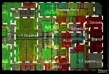
For most people, knowledge of a computer's device ends at the level of its constituent elements - a processor, a video card, RAM ... But what exactly happens inside these black rectangles after power is turned on is magic. In this article (most likely, even a series of articles) I will try to explain in simple language how these mysterious rectangles are arranged.
We assemble a computer from atoms
The path of knowledge, we begin almost from the lowest level of abstraction - from the level of atoms. We all know that almost all electronics are based on silicon, but why silicon?
In an amicable way, one needs to complete a full course of semiconductor devices, but I will set out the principal points that will allow us to see a more structured and clear picture of what is happening.
Orbitals and energy levels
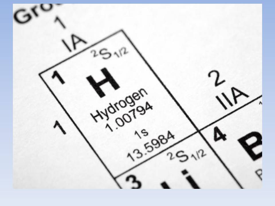 For example, take the simplest atom - hydrogen. The hydrogen nucleus consists of one proton and it has only one electron, which (simplify for clarity of presentation) rotates in a circular orbit.
 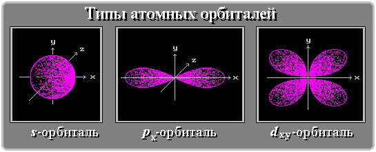 It would be more correct to say that the orbit is not circular, but spherical, that is, the electron creates a shell around the nucleus . According to the Pauli Principle , no more than two electrons can rotate in one such orbit in an atom. Orbitals are not only spherical (so-called S-orbitals), but also, for example, dumbbell-shaped (P-orbitals).
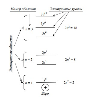
Orbitals form sublevels: for example, two S-orbitals form an S-sublevel that can accommodate two electrons; three P-orbitals form a P-sublevel; it can already fit 6 electrons due to the mutually perpendicular arrangement of orbitals in space. Already more electrons can be placed on the sublevels of the more complex orbitals (D, F, G, H, I - the sublevels contain 10, 14, 18, 22, 26 electrons, respectively).
The more complex the shape of the shell and the farther the electron from the nucleus, the more it has energy. The picture on the right shows an example of the energy levels that an electron can occupy in a single atom .
The last two words are not just highlighted: when neighboring atoms appear, the picture changes.
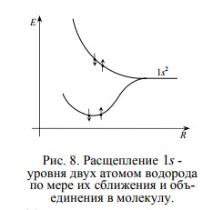 For example, if we start to bring together two hydrogen atoms, then the system, as we know, will tend to minimize energy. Therefore, to combine two separate hydrogen atoms into a H2 molecule, this should be energetically beneficial!
 And, indeed, the energy levels of the electrons of each atom are split, forming two sublevels — the upper and the lower, which become common to the now hydrogen molecules . As you can see, the lower sublevel has less energy than in a single hydrogen atom, so the electrons occupy it and form a molecule, pulling together the nucleus, like straps.
Atoms in a crystal
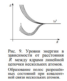 If we continue to increase the number of neighboring atoms, then within the extreme values of the energy of the split levels of two neighboring atoms, new energy states will appear (in the form of an additional fine structure). With a sufficiently large number of neighboring atoms (that is, in a crystal of a substance), the discrete allowed states merge into "bands" —the valence band, the conduction band, and the forbidden band , which many people know .
Charge carriers and conductivity
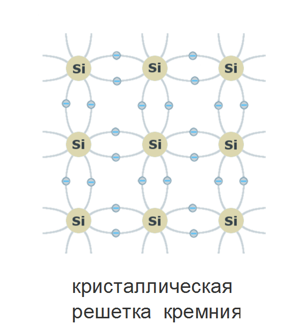 Electrons that have energy in the valence band do not participate in charge transfer through the crystal: they firmly “sit” in bonds, and in order for the electron to move through the crystal, it needs to take a higher energy level. This can be done by informing him of energy exceeding the width of the forbidden zone. At the same time, the covalent bond is broken, and a vacant place remains in the valence band - a positively charged “hole”.
 Silicon is at room temperature enough for the thermal vibrations of the crystal to break off the covalent bonds, forming free charge carriers — holes and electrons.
Semiconductors and dielectrics
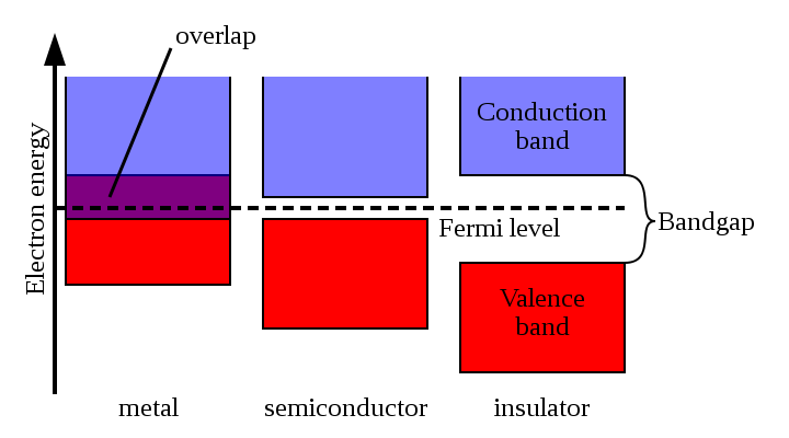 The characteristic values of the band gap in semiconductors are 0.1-4 eV. Crystals with a band gap of more than 4 eV are usually referred to as dielectrics.
Semiconductors p- and n-type
All this is fascinating, but it would be rather useless without doping with impurities.
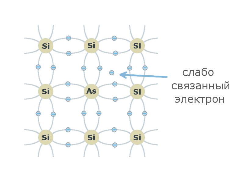 If the atom of the crystal lattice of tetravalent silicon or germanium is replaced by a pentavalent atom of the V element of the periodic table, then the four valence electrons of the impurity atom will be involved in the formation of covalent bonds. The fifth electron does not participate in the formation of covalent bonds, it is weakly bound to the nucleus and therefore can easily go into the conduction band and become a free carrier of charge , while leaving a stationary, positively charged ion . Such an impurity is called a donor, and the resulting semiconductor is an n-type semiconductor (negative).
If the atom of the crystal lattice of tetravalent silicon or germanium is replaced by a trivalent element, it can form only 3 of 4 covalent bonds in the lattice, since for the formation of the fourth it will need an electron from another covalent bond. In such a combination, a vacant place is formed — a mobile positively charged hole, while a fixed negatively charged impurity ion remains . Such an impurity is called an acceptor , and the resulting semiconductor is called a p-type semiconductor (positive).
Pay attention that own semiconductor, n-type or p-type semiconductor are electrically neutraland have an equal amount of positive and negative charges. The only difference is that in doped semiconductors, the “mirror” electrons and holes are charges — these are fixed impurity ions, firmly seated in the crystal lattice. In an undoped semiconductor, the number of free electrons is equal to the number of holes, while in a doped (for example, donor) number of electrons exceeds the number of holes, since most of them are replaced by fixed impurity ions.
Diode
If we now connect an n-type semiconductor with a p-type semiconductor, we get a diode. By the way, a real diode has little to do with its schematic representation, but that’s another story.
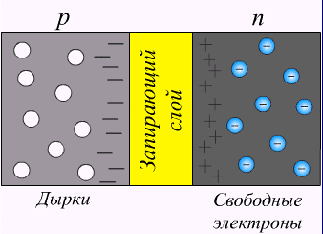 Consider what happens on the border of semiconductors. The n-semiconductor has a high electron concentration, and the p-semiconductor is low. Electrons, like gas, will begin to move (diffuse) from a region with a high concentration to a region with a lower concentration.
 Similarly, holes from p-semiconductor will be received.
Due to the displacement a diffusion current occurs.due to carrier concentration gradient. Moving across the border, mobile charge carriers expose stationary impurity ions, which create a “stopping”, oppositely directed field or, otherwise, compensating for the drift current .
In the absence of an external field, these currents balance each other. If the external field is applied in direction, it compensates for the field of stationary ions and opens the valve for diffusion current.
If the field is applied in the opposite direction, it enhances only the drift current, which is negligible compared to the diffusion current.
Thus, we get an element that conducts current in one direction and does not conduct in another.
Resistor-diode logic
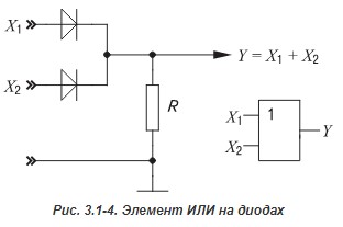
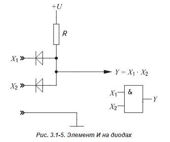
Since we are talking about digital technology, we note that with the help of a diode it is already possible to realize the logical elements AND and OR :
But to create a functionally complete system of logical functions, on the basis of which any logical function can be obtained, we cannot do without the element NOT .
To create this element, we need a transistor.
Transistor
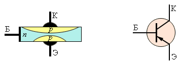
In fact, the transistor is a circuit of two diodes connected in opposite. In the absence of voltage on the middle electrode (base), the current between the other electrodes does not flow.
By creating a potential difference between the emitter (electrode with a high concentration of charge carriers) and a thin base, we create a stream of minority charge carriers from the emitter to the base, and in the case of a pnp transistor - holes.
Since the hole concentration in the emitter is increased, and the base is thin, its volume is filled with holes, and it turns from an n-type semiconductor into a p-type semiconductor, connecting the emitter and collector.
Inverter
By connecting the npn transistor as follows, we get an inverter: if there is a log 1 on the base, the transistor opens and connects the output to the ground - log 0. With log 0 on the base - the transistor is locked and the output is pulled to power - log 1.
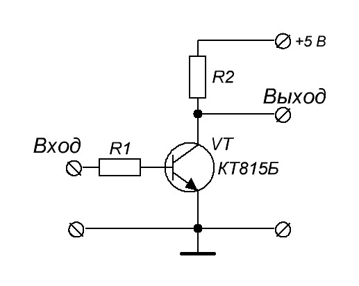
Thus, we get a voltage-controlled electronic key that allows you to create a logical element NOT , and, consequently, a functionally complete system of logical functions.
On this note we end up with physics, electrons and holes: we have everything we need to create a computing device.
How to make the logic elements calculate, memorize and execute instructions in the next article.
Black Friday 2017 - VDS in Moscow and Amsterdam