Methods for pairing electrical connections when tracing differential pairs on printed circuit boards
 The publication describes a method for pairing electrical connections when tracing differential pairs on printed circuit boards. The method is based on the technique of generating and applying patterns for connecting printed conductors of a differential pair to traced contacts of electronic components with minimizing the length of non-conjugated sections.
Introduction
Differential pairs are widely used for transmitting high-frequency and noise-protected signals in electronic devices implemented on the design of printed circuit boards. Each such signal is transmitted by a pair of equivalent signals of opposite polarity ( Signal + / Signal- ), and the receiver responds exclusively to the difference between their values. In this case, the external noise acting on the transmission lines (printed conductors) of the pair is added to the two signals inverted relative to each other without changing their difference and, thus, do not appear in the resulting signal on the receiver side.

The need to trace differential pairs in automatic or interactive modes led to the implementation in modern CAD REA tools for laying electrical connections (printed conductors) between given pairs of outputs - sources and receivers of signals, taking into account the given rules for the topology and parameters of these connections. The list of rules for tracing compounds in differential pairs is quite wide and diverse, the main ones among which are listed below.

Taking into account the given rules and restrictions, the means for tracing differential pairs carry out the laying of conductors with the maximum possible pairing and providing a difference of lengths not exceeding the specified design rules.
If necessary, a transition from layer to layer is allowed with the construction of the corresponding pair of interlayer transitions.
Pairing connections when tracing a differential pair
The sizes of the contact pads of the sources and receivers of signals, as well as the distances between them, significantly exceed the specified value of the nominal gap between the coupled conductors in differential pairs.
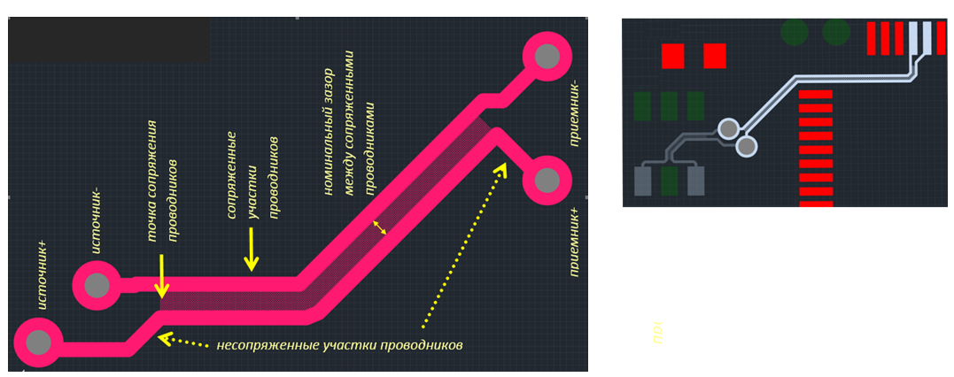
The first task to be solved when tracing a differential pair is the pairing of conductors, that is, the laying of their sections from the terminals of the components to the interface point. The quality of the pairing results is determined by the difference in the lengths of the constructed conductors and their symmetry. Symmetric pairing consists of a pair of conductors, in which one of them is a copy of the other, obtained as a result of applying the mirror image operation to it relative to the axis of symmetry of the contacts.
Asymmetric pairing consists of a pair of conductors of different lengths and with different topologies.

The proposed method of pairing compounds when tracing differential pairs is based on the use of pairing patterns. Each template contains a parameterized description of a pair of contacts and mating conductors emanating from these contacts.
It is assumed that pairs of contacts can be represented by the following printed wiring objects:
- round pads - planar or through leads of electronic components, as well as interlayer transitions
- rectangular contact pads - planar leads of electronic components
- segments of printed conductors.
The method of pairing conductors is considered on the example of round contact pads with the preservation of a common approach with respect to rectangular and other convex forms of contact pads.
Each pairing pattern is formed on the basis of the original one containing descriptions of a pair of contacts and mating conductors. All descriptions in the source template are presented in the local coordinate system and zero orientation. When placing each instance of the template on the board, operations of transferring to a given position Mv (X, Y) , rotation by a given angle Rot (θ) and mirroring RflOX () and RflOY () relative to the axes OX and OY, respectively, as shown on figure below.

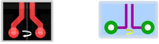
The description of the pair of contacts in the initial pairing template is performed using parametric approximation of the shape of the contact pads by closed polygons (for round pads, regular octagons are used as shown in the figure).
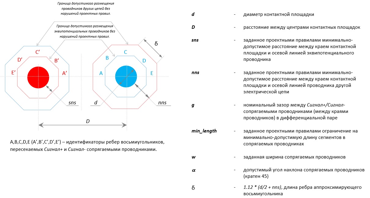
 Each instance of the original template is formed by a combination of a pair of polygon edges intersected by the mating Signal + and Signal-conductors. Enumeration of all valid combinations of edges forms a complete set of patterns of interfaces of conductors.
 In the following presentation, only the templates of the base subset are presented, the application of which the conversion operations RflOX () and RflOY () forms the complete set of conjugation patterns.
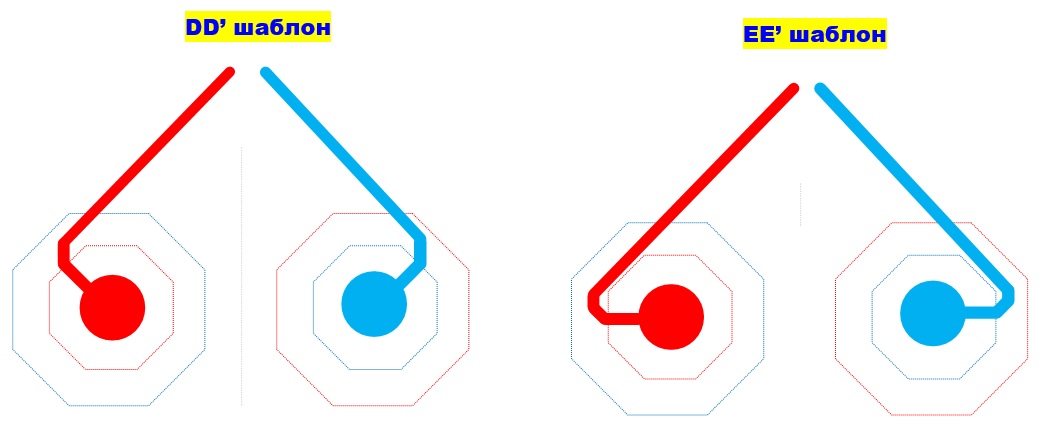
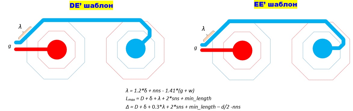
Symmetric Pairing Patterns
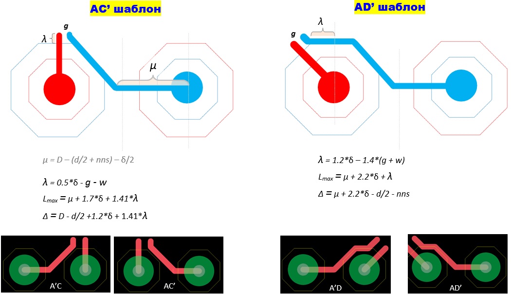
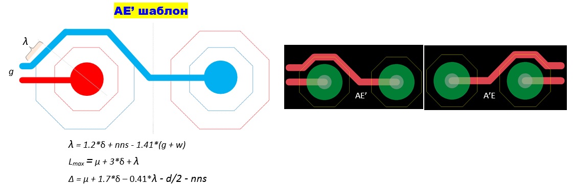
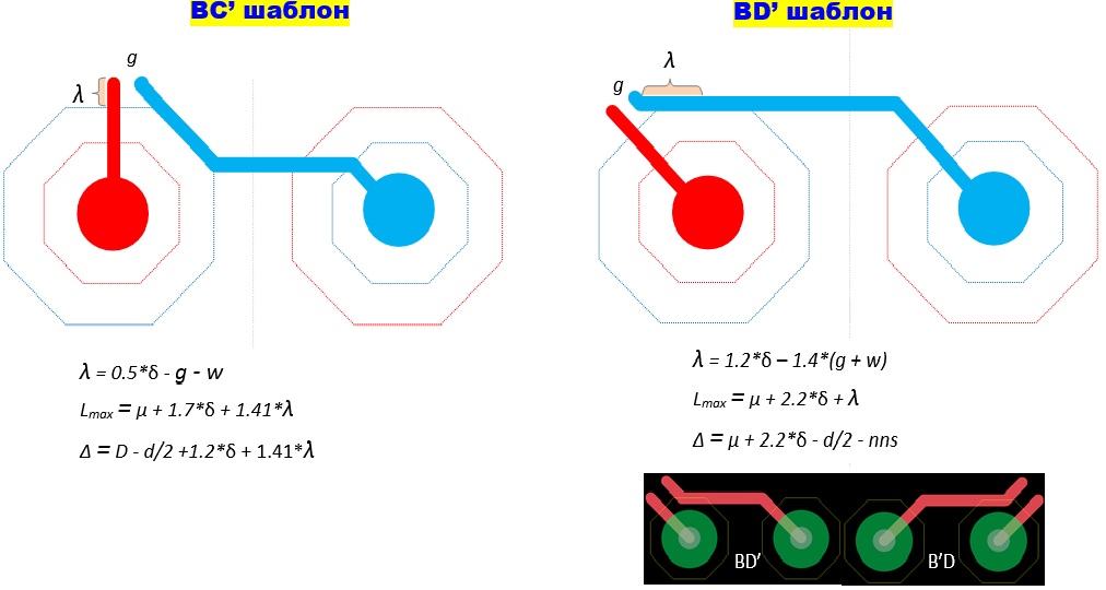
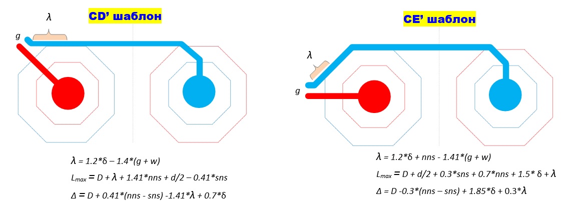
An important advantage of symmetric mating patterns is that the mating sections of the conductors are the same length. Next, the following parameters of each pairing pattern are evaluated:
- the value of the template settings parameter (λ) to ensure the specified design rules
- maximum length of mating conductors (Lmax)
- the difference in lengths (modulo) of the mating conductors (Δ)

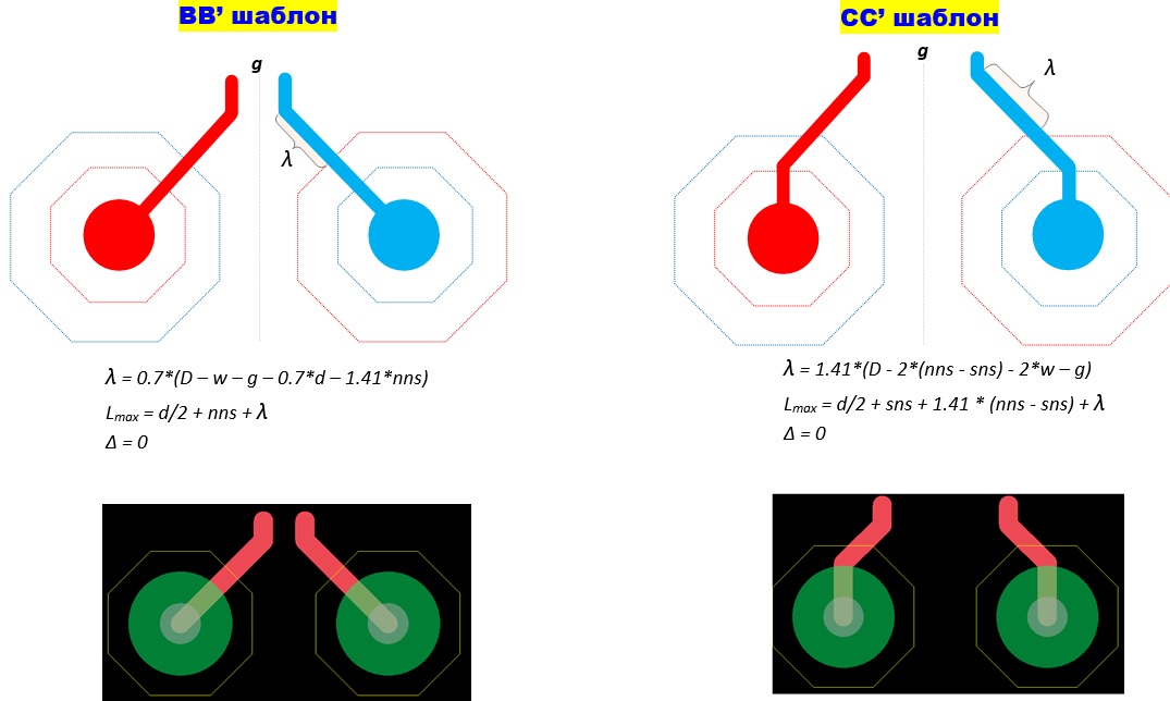
The two symmetric pairing patterns presented below are of limited use in cases where any printed wiring elements are directly placed in front of a pair of contact pads that interfere with the pairing of conductors while minimizing their total length.
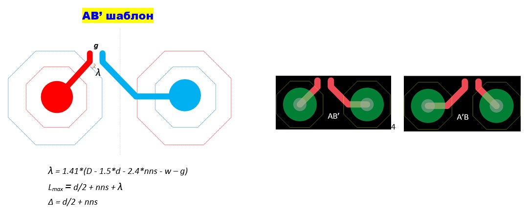
Asymmetric mating patterns
When tracing boards with a high density of printed circuit boards, the use of symmetric patterns in many situations is impossible without violating design rules. For this reason, many of them are expanded by asymmetric patterns, in which the mating conductors have different lengths. The left-side variants of asymmetric pairing patterns are presented below, the right-side patterns are obtained as a result of applying a mirror image to the OY axis for the operation , for example: A'B = RflOY (AB ') .

The presented many interface patterns (including derivatives obtained as a result of applying the conversion operations RflOX () and RflOY () to the base set) is applicable to any pair of traced contacts.
In the process of tracing a differential pair of contacts for each interface point (determined by the current position of the mouse cursor or calculated automatically), the following operations are performed:

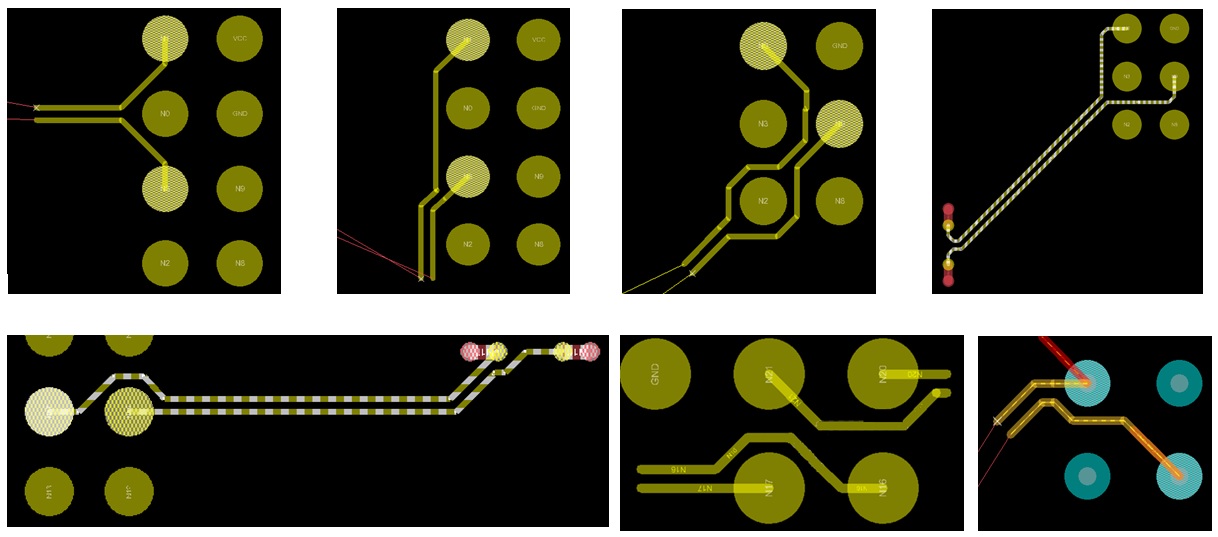
Below are illustrations of the choice of pairing patterns by region when tracing a pair of contacts of a differential circuit.


Watch the video >>>
A few examples of laying differential pair connections using pairing patterns.
Brief conclusions
- Conjugation of conductors when tracing differential pairs requires the use of special methods to minimize the total length of non-conjugate sections.
- The solution of the problem of pairing conductors is performed both on the “ side ” of a pair of contacts - signal sources, and on the “ side ” of contacts - receivers.
- The use of conductors pairing templates is not the only method for solving this problem, however, it has high speed (due to localization of the analyzed area of the printed circuit board mounting space) and provides a choice of the most suitable conductors pairing options.

- The composition of the used interface patterns can be expanded with options that provide, if necessary, compensation for the total length difference of the Signal + / Signal connections in the differential pair due to the forced increase in the length of the short pair pair.