CCD ruler: what it is eaten with
In this article I want to present my experience in using a linear CCD photodetector. Such a CCD line can be used in the design of a makeshift spectrometer, barcode reader, position sensor or deviation of the laser beam, a scanner for photo or film, and much more. In my case, it was a laser scanner, which I can’t describe on the network.
What is a charge-coupled device?
Most often, when talking about CCD, they mean various photodetectors. Less commonly, these are memory devices: shift registers, delay lines. At its core, this device is somewhat reminiscent of the memory on cylindrical magnetic domains, only on silicon - with the help of a traveling wave of an electric field created by a system of electrodes, clumps of charge carriers that have somehow formed in it earlier move through the semiconductor. Thus, we get a shift register that has an extremely simple structure and is able to remember not only a sequence of digital units and zeros, but also an analog signal.

In the CCD image receivers, it is precisely this ability of this structure that is used to sequentially output the charges accumulated under each of the pixels of the structure. In addition, the same gate system that is used to move the charges during exposure creates potential wells in which these charges accumulate (or these holes are created during the formation of the structure - similar to the built-in and induced channels of the MOS transistor). More complex structures include a resistive gate along which a smooth potential slope is formed (this is how the Hamamatsu S11155 CCD lines are arranged), as well as the separation of charge accumulation and transfer zones - the accumulated charges of the entire line are first transferred to the buffer line and then subsequently advanced exit along the last.
The simplicity of the internal structure translates into the complexity of managing it. Even the simplest version of the CCD line requires the generation of a two-or three-phase signal of complex shape with different voltage levels with steep edges (with a high input capacitance of 1000 pF or more), shifted relative to each other. Hamamatsu S11155 type rulers require as many as eight different signals with different levels of high and low voltage on both sides of zero.
Fortunately, some companies (for example, Sony) released a line in which all this complexity is formed directly on the chip. And for their work, you need to generate only two signals: the opening electronic shutter for the duration of the exposure, and the clock. In our design, this is exactly the ILX554 line: it (as a rule, used, but quite functional) is easy to purchase from the Chinese on Aliexpress.
Let's look at the datasheet.
And we see that only 6 of the 22 pins are involved. This is + 5V power supply, ROG and CLK input signals, Vout output signal, SHSW mode select input and ground. And it's all.
ROG is the electronic shutter control (and the start of charge transfer from the photosensitive line to the direct shift register). He has an active level - zero. To expose the matrix, it must be pressed to zero and held for as long as necessary - from 5 μs to several seconds. And then, letting go, wait at least 3 μs (during this time, the charge transfer circuit works out). All this time at the entrance of CLK we keep a high level. And then you can read the line, applying to the CLK input a meander with a frequency from several tens of kilohertz to 2 MHz. In this case, at each difference from unity to zero, the next pixel will be pushed to the output. There are 2088 such pixels in the lineup, of which 2048 are working, photosensitive (in reality, it’s several more, but the outermost pixels are partially obscured).
And how it will be pushed depends on what is at the input of SHSW. If it is a logical unit, then the output will produce a rather intricate signal:
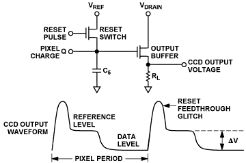
Moreover, when the CLK goes from zero to one, a reset occurs, and from unity to zero - the issuance of a useful signal.
And at zero at the SHSW input, the built-in sampling-storage circuit is turned on, which simplifies this signal to a simple step-by-step video signal, where with each new transition of CLK to zero, the signal level of the next pixel simply appears and is held for the entire period of the CLK signal.
The useful range of the output signal comes from a certain dark level, which according to the datasheet is 2.85 V, but in reality it can be different (in my line - about 3 V), and when saturated, the output signal level drops to 1.5-2 B.
In general, that's all we need to know about this line.
Inclusion circuit
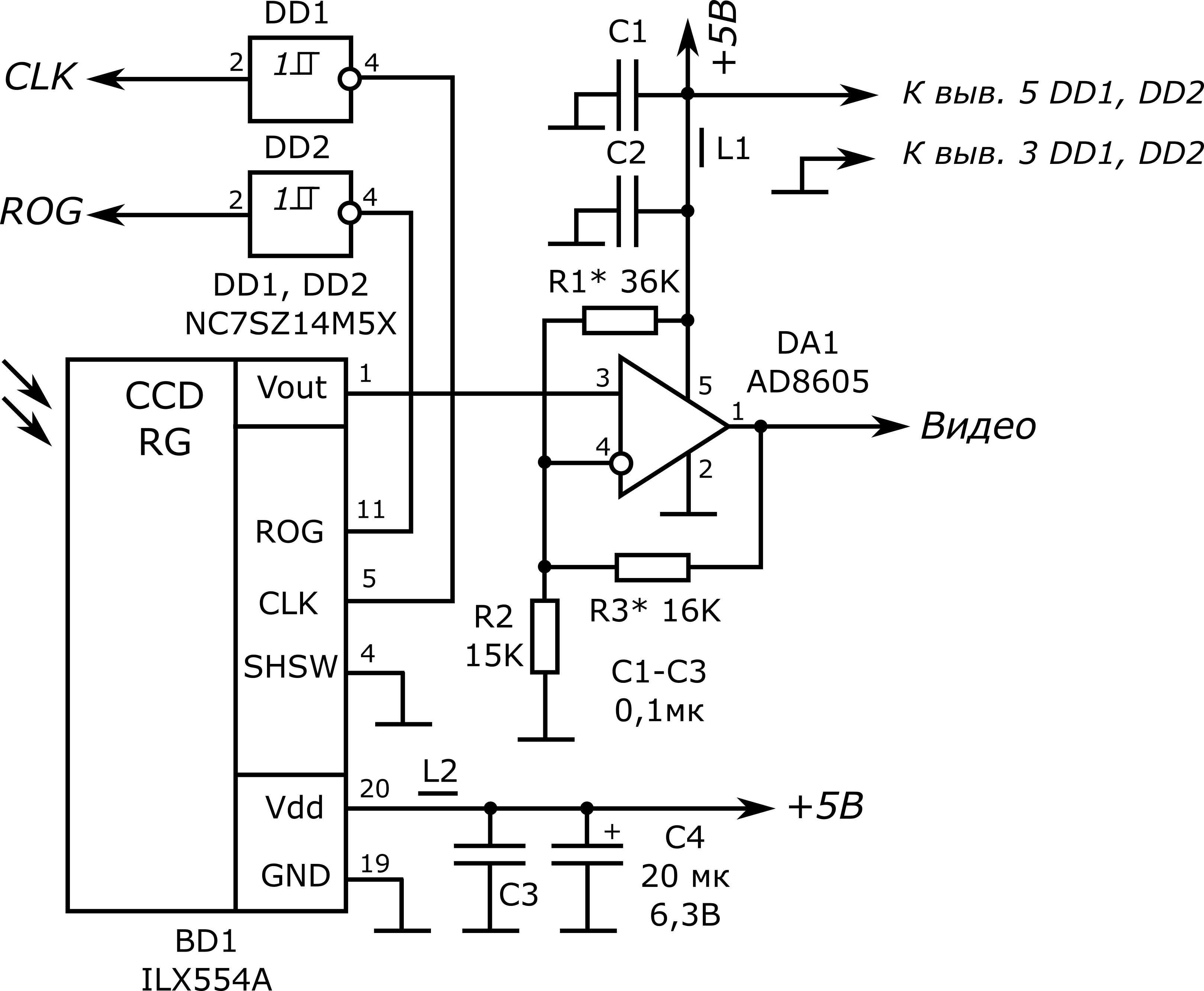
It is simple and obvious. We generate CLK and ROG signals programmatically using MK, and Schmitt triggers at the input are the simplest way to switch from 3.3 V to 5 V. The fact is that there are no buffers in these lines in the line, and for the matrix circuits to work correctly you need to submit to them a meander with a full scale from zero to five volts and a good steepness of the fronts. The NC7SZ14M5X indicated on the diagram are very convenient single Schmitt inverting triggers with steep fronts and increased load capacity, and I often use them in my projects.
Using DA1, the video signal level from the lineup “accelerates” to the range in which the ADC operates, while the “stand” of approximately 1.5 V corresponding to the saturation level is removed. Since the difference between the signal amplitude and the “stand” value varies greatly between different CCD line arrays, the resistances R1 and R3 should be selected by “laying” the output signal in the required range. It should be borne in mind that not only the displacement, but also the gain depends on the resistance R1, so you must first select it.
L1 and L2 are ferrite beads or small chokes for 1-2 μG of frame size 0805 or 0603. Resistors and capacitors are used of the same size. The circuit is assembled on a double-sided board by surface mounting. I do not bring the board layout, since I still have a lot of things on it.
Software implementation on MK
The MK task is to generate a high-level ROG signal (do not forget about inverters!) Of the required duration, then a short (3-10 μs) pause, and after it a sequence of 2090 high-level pulses separated by equal pauses in duration. During these pulses (or pauses), some time after the front, the pixel illumination value is taken using an on-board or external ADC. After reading the frame, you must also pause until a new ROG pulse - the same 3-10 μs. After turning on the power and, as it turned out, after a long (more than 100 ms) non-use of the ruler, you need to “clean it” by applying a free standard pulse train to the CLK a couple of times.
On STM32, it is wise to do all this on a timer interrupt. By setting the timer to generate interrupts with a frequency corresponding to a doubled pixel frequency, we get each timer operation into an interrupt, where we alternately output zero or one to the port, and when we output zero, then we read the readings from the ADC. And after counting 2090 cycles, we stop the timer. To read the next frame, you need to reset the cycle counter to zero, start the timer and wait until everything is counted.
Something like this, as shown in these code snippets.
bool clkState = false;
bool frameOk = true;
uint16_t pixCount = 0;
uint16_t ccdFrame[2090];
inline uint16_t readADC1(void)
// Тут у нас зависящая от конкретного МК реализация чтения из АЦП
{
     .
     .
     .
}
void Delay(unsigned int Val)
// Функция для небольших задержек
{
    for( ; Val != 0; Val--)
        __NOP();
}
void readCCD(void)
// Запуск считывания ПЗС-линейки
{
    pixCount = 0;                      // Обнулили счетчик пикселов
    frameOk = false;                 // Сбросили флаг
    TIM_Cmd(TIM6, ENABLE);    // Запустили таймер
    while(frameOk == false);     // Стоим, пока флаг не взведется
}
// ... всякий разный код ... //
void TIM6_IRQHandler(void)
/*
Здесь мы оказываемся раз в сколько-то микросекунд и
формируем меандр CLK и в нужные моменты запускаем АЦП
*/
{
	if (TIM_GetITStatus(TIM4, TIM_IT_Update) != RESET)
        {
		if(clkState == true)
                // Формируем паузу (лог.0) и здесь же запускаем АЦП
		{
		    clkState = false;
		    GPIOB->ODR &= ~GPIO_ODR_ODR_1; // выводим в порт логический ноль
		    Delay(3); // Небольшая пауза, пока не закончатся помехи и переходные процессы
		    ccdFrame[pixCount] = readADC1();
		}
		else
                // Формируем импульс (лог.1)
		{
		    pixCount++;
		    clkState = true;
		    GPIOB->ODR |= GPIO_ODR_ODR_1; // Выводим в порт логическую едииницу
		}
		if(pixCount >= 2090)
                // Дошли до конца линейки, выставили флаг и остановили таймер
		{
		    pixCount = 0;
                    frameOk = true;
		    TIM_Cmd(TIM6, DISABLE);
		}
                TIM_ClearITPendingBit(TIM4, TIM_IT_Update);
        }
}
And here is the result.
The result is not bad. Despite the fact that the built-in ADC does not have any characteristics, its noise characteristics fully correspond to the noise of the CCD line. The noise track of the dark signal with an accumulation time of about 1 ms turns out to be ~ 3-4 quantization levels, and when using an external 14-bit ADC with excellent characteristics, the results are only slightly better. With the increase in illumination, noise increases for a simple reason: the number of photoelectrons in each of the pixels is not so large (according to my calculations, about 30 thousand at saturation). For the best devices, this value reaches 200 thousand.
On the chart below is an example of a “picture” registered by the ruler, on which against the background of the illuminated wall there is a dark stand on which a glass hollow ball with a diameter of 1 cm fixed inside is filled with black solution. A peak is a reflection from the outer surface of this ball. The noise in bright areas is the structure of the wall itself, reinforced by speckles from the laser, from frame to frame it remains stationary. The real line noise is much less.

Other similar
arrays Some other 2048-pixel black and white SONY CCD arrays by the ILX511, ILX551 (the latter has a different pinout and requires two supply voltages - 5 and 9 V), differing in transverse pixel size (from 14 to 200 μm) and spectral sensitivity (ILX554A is red- and IR-sensitive, similar to index B has a reduced sensitivity in the IR region and is closer in sensitivity to the eye, and ILX511B is more blue-sensitive). Their dynamic characteristics are different: the ILX551B's dynamic range due to the small pixel size reaches 6000 (our line reaches this DD with short shutter speeds of about 10 μs).
* * *
This article discusses the connection of perhaps the easiest to use CCD line. This simplicity is due to the fact that all the complexity is hidden in her under the hood. If it weren’t for the built-in drivers, I would have to generate a lot of multilevel signals.
Unfortunately, by modern standards, such a CCD line with built-in drivers have not the best characteristics. So, in this line, the dynamic range, defined as the ratio of the saturation signal to the dark signal, is 333: 1, and defined as the ratio of the saturation signal to the minimum signal detected against the background of noise - about 1000: 1. But such devices are not only difficult to use, but often difficult to access (the same Hamamatsu requires complex bureaucratic formalities when purchasing its CCD arrays and other photodetectors due to the dual purpose of these products). However, such high performance is not always required, and for many purposes the parameters of these devices are quite acceptable.