Development of the simplest “firmware” for FPGAs installed in Redd, and debugging using the memory test as an example
Somehow I can’t express my thoughts briefly. Last fall, there was a desire to tell in more detail about the PSoC architecture that I mastered, which resulted in a series of articles about it. Now I am participating in the preparation of the hardware for our Redd remote debugging complex, which was described here , and I want to throw out the accumulated experience in text form. I’m not sure yet, but it seems to me that again it’s not one article, but a cycle. Firstly, this is how I will document the developed methods of development that may be useful to someone both when working with the complex, and in general, and secondly, the concept is still new, not quite established. Perhaps, in the process of discussing articles, some comments will appear, from which one can draw something to expand (or even change) it. Therefore, we proceed.
I don’t really like to theorize, preferring to lay out some practical things at once. But at the beginning of the first article, without a long introduction anywhere. In it, I justify the current approach to development. And everything will revolve around one thing: man-hour is a very expensive resource. And the matter is not only in the terms allotted for the project. He is physically expensive. If it is spent on the development of the final product, well, what can you do without it nowhere. But when it is spent on auxiliary work, this, in my opinion, is bad. I remember that I had a dispute with one developer who said that having made prototypes on his own, he would save money for his native company. I made the argument that he would spend about 3 days on the manufacture. That is 24 man-hours. We take his salary for these hours, add the social tax that "the employer pays", as well as the rental of the office for these hours. And we are surprised to see that ordering boards on the side, you can get lower costs. But that's me, I exaggerate. In general, if labor costs can be avoided, they should be avoided.
What is the development of “firmware” for the Redd complex? This is an auxiliary job. The main project will live happily ever after; it should be done as efficiently as possible, with excellent optimization, etc. But spending time and energy on auxiliary things that will go to the archive after development is wasteful. It was with an eye on this principle that the development of Redd equipment was carried out. All functions, if possible, are implemented as standard things. The SPI, I2C and UART buses are implemented on standard FTDI microcircuits and are programmed through standard drivers, without any frills. Management of reels is implemented in the format of a virtual COM port. It can be modified, but at least everything has been done so that such a desire does not arise. In general, everything standard, if possible, is implemented in a standard way. From project to project, developers simply need to quickly write typical code for the PC to access these buses. The development technique in C ++ should be obvious to those who develop programs for microcontrollers (we will talk about some technical details in another article).
But FPGA stands alone in the complex. It is added to the system for cases when it is necessary to implement any non-standard protocols with a high performance requirement. If those are required, you will have to do the “firmware” for it. That's about FPGA programming and I want to talk specifically, just all for the same purpose - to reduce the development time of auxiliary things.
In order not to confuse the reader, I will formulate the thought in a frame:
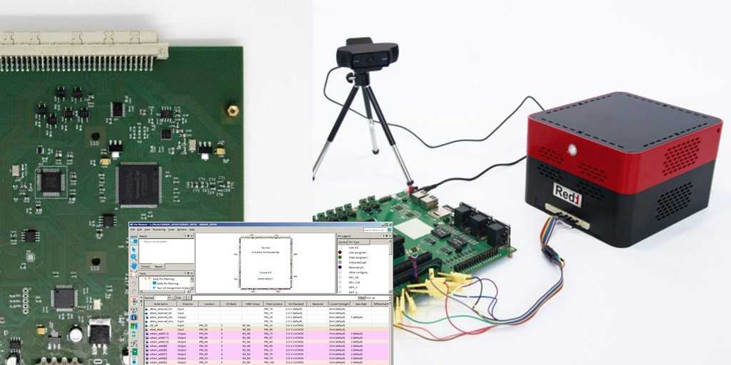
Let's look at the block diagram of the complex

At the bottom of the circuit is a “calculator”. Actually, this is a standard PC with Linux. Developers can write regular programs in C, C ++, Python, etc., which will be executed by the computer. In the upper right part are the standard ports of standard tires. On the left is a switch for standard devices (SPI Flash, SD card and several low-current solid-state relays, which can, for example, simulate button presses). And in the center is precisely that part, the work with which is planned to be considered in this series of articles. Its heart is an FPGA class FPGA, from which straight lines go out (can be used as differential pairs or ordinary unbuffered lines), GPIO lines with a configurable logic level, as well as a USB 2.0 bus implemented through an ULPI chip.
When developing high-performance control logic for FPGAs, usually His Majesty is played the first violin by a state machine. It is on the machines that it is possible to implement high-speed, but complex logic. But on the other hand, an automaton is developed more slowly than a program for a processor, and its modification is another process. There are systems that simplify the development and maintenance of machines. One of them was even developed by our company, but still, the design process for any kind of complex logic is not fast. When the developed system is the final product, it makes sense to prepare, design a good control machine and spend time on its implementation. But as already noted, development for Redd is an auxiliary job. It is designed to facilitate the process, not complicate it. Therefore, it was decided
But on the other hand, when developing the hardware, the most fashionable option to date, FPGA with the ARM core, was rejected. Firstly, for price reasons. A Cyclone V SoC-based prototype board is moderately expensive, but oddly enough, a separate FPGA is much more expensive. Most likely, the price of prototyping boards is dumped in order to lure developers to use FPGA data, and the boards are sold individually. The series will have to take individual chips. But in addition, there is also a "second". Secondly, when I was experimenting with Cyclone V SoC, it turned out that this processor system is not so and is productive when it comes to single access to ports. Batch - yes, there work is fast. And in the case of single accesses at a clock frequency of the processor core of 925 MHz, you can get access to the ports at a frequency of a few megahertz. To everyone, I propose to call up the standard function of entering data into the FIFO of the UART block, which checks the queue overflow, but calling it when the queue is obviously empty, that is, nothing interferes with the operations. My productivity went from one million to five hundred thousand calls per second (of course, working with the memory went at normal speed, all the caches were tuned, even the function variant that did not check FIFO for overflow worked faster, just the function under discussion has abundantly mixed write and read from ports). This is FIFO! In fact, FIFO was invented in order to drop data there and forget! Quick quit! And not with performance, less than one mega-operation per second at a processor frequency of 925 MHz ... which checks the queue overflow, but calling it when the queue is obviously empty, that is, nothing interferes with the operations. My productivity went from one million to five hundred thousand calls per second (of course, working with the memory went at normal speed, all the caches were tuned, even the function variant that did not check FIFO for overflow worked faster, just the function under discussion has abundantly mixed write and read from ports). This is FIFO! In fact, FIFO was invented in order to drop data there and forget! Quick quit! And not with performance, less than one mega-operation per second at a processor frequency of 925 MHz ... which checks the queue overflow, but calling it when the queue is obviously empty, that is, nothing interferes with the operations. My productivity went from one million to five hundred thousand calls per second (of course, working with the memory went at normal speed, all the caches were tuned, even the function variant that did not check FIFO for overflow worked faster, just the function under discussion has abundantly mixed write and read from ports). This is FIFO! In fact, FIFO was invented in order to drop data there and forget! Quick quit! And not with performance, less than one mega-operation per second at a processor frequency of 925 MHz ... working with memory at that went at normal speed, all caches were configured, even the function variant that did not check FIFO for overcrowding worked faster, just in the discussed function there are plentifully mixed writes and reads from ports). This is FIFO! In fact, FIFO was invented in order to drop data there and forget! Quick quit! And not with performance, less than one mega-operation per second at a processor frequency of 925 MHz ... working with memory at that went at normal speed, all caches were configured, even the function variant that did not check FIFO for overcrowding worked faster, just in the discussed function there are plentifully mixed writes and reads from ports). This is FIFO! In fact, FIFO was invented in order to drop data there and forget! Quick quit! And not with performance, less than one mega-operation per second at a processor frequency of 925 MHz ...
Latency is to blame. Between the processor core and the equipment is located from three bridges or more. Moreover, the speed of access to the ports depends on the context (several records in a row will go quickly, but the first reading will stop the process until the cached data is completely unloaded, too many records in a row will also slow down, since the write buffers are exhausted). Finally, examining the traces accumulated in the debugging buffer showed that the Cortex A architecture can execute the same part for a different number of clock cycles due to the complex cache system. In sum, looking at all these factors (price, performance drawdowns when working with equipment, instability of access speed to the equipment, general dependence on the context), it was decided not to put such a chip in the complex.
Experiments with Cypress's PSoC showed that there the Cortex M core gives more predictable and repeatable results, but the logical capacity and maximum operating frequency of these controllers did not correspond to the technical specifications, so they were also discarded.
It was decided to install an inexpensive typical Cyclone IV FPGA and recommend the use of a synthesized NIOS II processor core. Well, and if necessary - to conduct development using any other methods (automatic machines, hard logic, etc.).
If the Redd complex is running Linux, this does not mean that development should be carried out in this OS. Redd is a remote executor, and development should be carried out on your computer, whatever the OS. Whoever has Linux is all the easier, but who is used to Windows (I used to dislike WIN 3.1 very much, but I was forced to work, but somewhere by the time of WIN95 OSR2 I got used to it, and now it's useless to deal with it, it's easier to accept) , those can continue to lead development in it.
Since my friendship with Linux did not work out, I will not give step-by-step instructions for setting up the environment under it, but I will limit myself to general words. Who works with this OS will be enough for that, and the rest ... Believe me, it’s easier to contact system administrators. In the end, I did just that. But nonetheless.
You should download and install Quartus Prime Programmer and Tools of the same version as your development environment. If versions do not match, there may be surprises. I spent the whole evening to comprehend this fact. Therefore, just download the tool of the same version as the development environment.
After installation, enter the directory where the program was installed, the bin subdirectory. In general, the most important file should be jtagconfig. If you run it without arguments (by the way, I persistently demanded to enter ./jtagconfig and only so), then a list of programmers available in the system and FPGAs connected to them will be displayed. There should be a USB Blaster. And the first problem that the system throws up is not enough access rights to work with USB. How to solve it without resorting to sudo is described here:radiotech.kz/threads/nastrojka-altera-usb-blaster-v-ubuntu-16-04.1244
But here is a list of devices displayed. Now you should write:
after which the server is launched, accessible from anywhere from the network.
Everything would be fine, but the system firewall will not let anyone see this server. A check on Google showed that for each type of Linux (of which there are many), the ports in the firewall open in their own way, and so many spells must be cast that I prefer to contact the admins.
It is also worth considering that if jtagd was not registered in autorun, then when you open remote access, you will be told that it is impossible to set a password. To prevent this from happening, jtagd must be started not by means of jtagconfig itself, but before it.
In general, shamanism is on shamanism. Let me just fix the thesis:
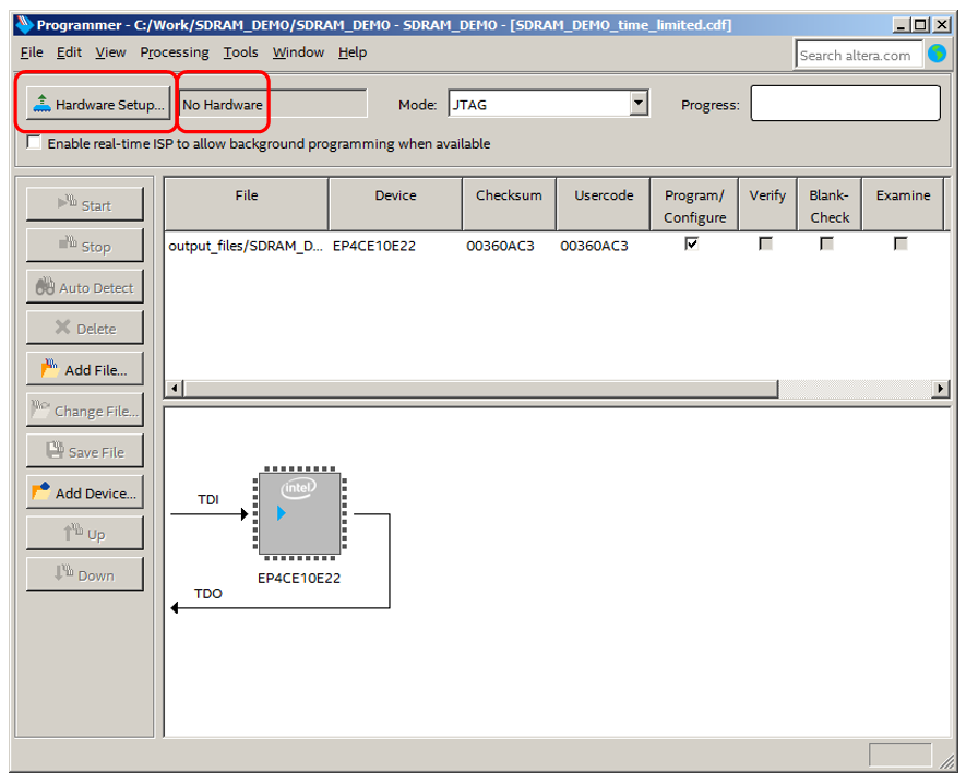
There is, of course, a similar path that goes through the GUI interface, but it’s more logical to do everything in batch. Therefore, I described a batch version. When all these theses have been completed (and the system administrators have completed them), we launch the programmer on our machine, we see a message about the lack of equipment. Click Hardware Setup:
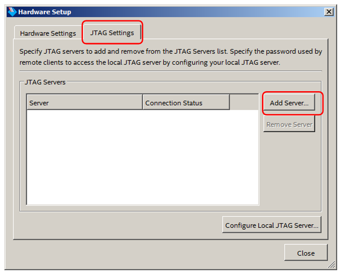
Go to the JTAG Settings tab and click Add Server:
Enter the network address of Redd (I have 192.168.1.100) and password:

Make sure the connection is successful.
I spent three May holidays to achieve this, and then administrators decided everything.

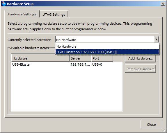
Switch to the Hardware Settings tab, open the drop-down list and select the remote programmer there:
That's it, now you can use it. The Start button is unlocked.
Well. For the article to have real practical value, let's analyze the simplest “firmware” made using the above methods. The simplest thing that I really managed to implement for the complex is a test of the SDRAM chip. Here on this example and practice.
There are a number of amateur cores to support SDRAM, but they all turn on somehow tricky. And accounting for all the tricks is labor. We will try to use ready-made solutions that can be inserted into the NIOS II computing system, so we will use the standard SDRAM Controller Core. The core itself is described in the Embedded Peripherals IP User Guide., and a lot of space in the description is devoted to the clock shift for SDRAM relative to the core clock. Complex theoretical calculations and formulas are given, but what to do is not particularly reported. What to do can be found in the document Using the SDRAM on Altera's DE0 Board with Verilog Designs . In the course of the analysis, I will apply the knowledge from this document.
I will be developing in the free version of Quartus Prime 17.0. I focus on this, since during the assembly, they tell me that in the future, the core of the SDRAM Controllerwill be kicked out of the free version. If this has already happened in your development environment, no one bothers to download the free 17th version and install it on a virtual machine. The main work is done wherever you are used to, and the firmware for Redd with SDRAM is in the 17th version. Well, that’s if you use the free options. Nobody threatened to throw it out of paid ones yet. But I was distracted. Create a new project:

Call it SDRAM_DEMO. The name should be remembered: I'm going to carry out superfast development, so the processor system itself should be at the top level, without any Verilog-layers. And for this to happen, the name of the processor system must match the name of the project. So remember it.

Agreeing with the default values in a few steps, we come to the choice of a crystal. We select the EP4CE10E22C7 used in the complex.

In the next step, out of habit, I choose modeling in ModelSim-Altera. Today we will not model anything, but everything can come in handy. It is better to develop such a habit and follow it:
The project is created. Immediately go to the creation of the processor system (Tools-> Platform Designer):
We created a system containing a clock and reset module:

But as I mentioned, a special clock is required for the SDRAM kernel. Therefore, the standard module is ruthlessly thrown out
And instead of it we add the University Program-> System and SDRAM Clock for DE-series boards block:
In the properties, select DE0-Nano, as the inspiration for the SDRAM switching circuit was drawn from this breadboard:

We begin to fill our processor system. Of course, the first thing to add to it is the processor core itself. Let it be Processor And Peripherals-> Embedded Processors-> NIOS II Processor.
For him, we do not fill out any properties yet. Just click Finish, even though we have formed a series of error messages. So far, there is no equipment that will eliminate these errors.
Now add the actual SDRAM. Memory Interfaces and Controllers-> SDRAM-> SDRAM Controller.
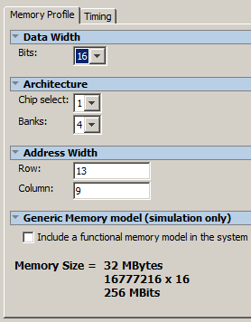
Here we have to hold on to filling out the properties. Select the nearest microcircuit similar in organization from the list and click Apppy. Its properties fall into the fields Memory Profile:
Now we change the bit width of the data bus by 16, the number of address lines - by 13, and the columns - by 9.
I still do not correct the times, perhaps in the future this recommendation will be changed.
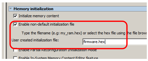
The processor system implies a program. The program must be stored somewhere. We will test the SDRAM chip. At the moment, we cannot trust her. Therefore, to store the program, add memory based on block RAM FPGA. Basic Functions-> On Chip Memory-> On-Chip Memory (RAM or ROM):

Volume ... Well, let it be 32 kilobytes.

This memory must be loading from somewhere. For this to happen, check the Enable non-default initialization file box and enter some meaningful file name. Let's say firmware.hex:
The article is already complicated, so we won’t overload it. We will simply output the physical result of the test in the form of PASS / FAIL lines (and we will see the logical result with my favorite JTAG debugging). To do this, add the GPIO port. Processors and Peripherals-> Peripherals-> PIO (Parallel IO):
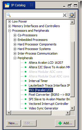
Set 2 bits in the properties, I also like to check the box for individual bit control. Also just a habit.

We got such a system with a bunch of errors:

We begin to eliminate them. To begin with, we will break the clock and reset. At the clock and reset unit, the inputs must be thrown out. To do this, there are fields that say "Double-click to export":

Click, but give more or less short names.

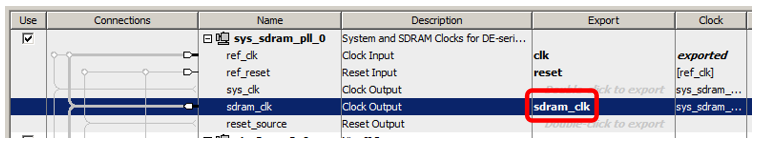
You also need to throw out the SDRAM clock output:
Now we split sys_clk to all clock inputs, and reset_source to all reset lines. You can gently hit the points connecting the corresponding lines with the “mouse”, or you can go to the corresponding exit, click the right mouse button, and then go to the Connections submenu in the drop-down menu and select the connections there.

Then we connect the tires together. We connect Data Master to all buses of all devices, and Inctruction Master - to almost all. It is not required to connect it to the PIO_0 bus. From there, instructions will definitely not be read.

Now you can resolve address conflicts. To do this, select the menu item System-> Assign Base Addresses:

And when we got addresses, we can also assign vectors. To do this, go to the properties of the processor core (point to it, press the right mouse button and select the Edit menu item) and configure the vectors on Onchip Memory there. Just select this type of memory in the drop-down lists, the numbers will be substituted themselves.

No errors left. But two warnings remain. I forgot to export the SDRAM and PIO lines.

As we already did this for the reset and clock block, double-click on the required legs and give them the shortest (but understandable) names:

Everything, there are no more errors or warnings. Save the system. Moreover, the name must coincide with the name of the project, so that the processor system becomes an element of the top level in the project. Have not forgotten what we called it?


Well, we press the most important button - generate HDL.

Everything, the processor part is created. Click Finish. We are reminded that it would be nice to add this processor system to the project:

Add:

And there, using the Add button, we achieve the following picture: A
SIP file has not yet been created. Yes, and we do not need it in the framework of this article.
Uhhhh The first step has been taken. We draft the project so that the system finds out the project hierarchy and the legs used. Compilation errors are not scary. Just in the free version of the environment, kernels were created that work only while the JTAG adapter is connected. But in the Redd complex, it is always connected, as it is divorced on a common board, that is, we have nothing to fear. So we ignore these errors.

Now back to the description of the SDRAM kernel. It says that the CKE line is not used and is always connected to the unit. In fact, within the framework of the complex, FPGA legs are not just expensive, but a precious resource. And it would be foolish to spread the leg, which is always in the unit (and on the DE0-NANO board it is also not divorced). There would be a Verilog-layer, the corresponding chain could be cut there, but I save time (nervous laughter, looking at the volume of the already obtained document, but without saving it would have turned out even more). Therefore, there is no layer. How to be Go to the Assignment Editor. It is in it, since in Pin Planner, judging by the descriptions, there is no similar functionality.

There is still no line. Good. Create a new one.

Select the following icon:

In the search system we set, click List and in the search results we find our CKE:
Add it to the right column, click OK.
We

get the following list: In the yellow field, click on the drop-down list and find Virtual Pin. We choose. Yellowness moved to another cell:

There we choose On:
That's it, yellowness is gone. And the chain is now marked as virtual, which means that it does not require a physical leg. Therefore, we can not assign it to the physical conclusion of the FPGA. Close the Assignment Editor, open the Pin Planner. You can assign the legs, referring to the figure, or you can take the list from the * .qsf file, which is part of the project, which I will attach to the article.

That's it, close Pin Planner, we carry out the final compilation of the project. The hardware is ready, we proceed to the development of the software for the resulting processor system. But the article turned out so huge that we will do it next time .
Long introduction
I don’t really like to theorize, preferring to lay out some practical things at once. But at the beginning of the first article, without a long introduction anywhere. In it, I justify the current approach to development. And everything will revolve around one thing: man-hour is a very expensive resource. And the matter is not only in the terms allotted for the project. He is physically expensive. If it is spent on the development of the final product, well, what can you do without it nowhere. But when it is spent on auxiliary work, this, in my opinion, is bad. I remember that I had a dispute with one developer who said that having made prototypes on his own, he would save money for his native company. I made the argument that he would spend about 3 days on the manufacture. That is 24 man-hours. We take his salary for these hours, add the social tax that "the employer pays", as well as the rental of the office for these hours. And we are surprised to see that ordering boards on the side, you can get lower costs. But that's me, I exaggerate. In general, if labor costs can be avoided, they should be avoided.
What is the development of “firmware” for the Redd complex? This is an auxiliary job. The main project will live happily ever after; it should be done as efficiently as possible, with excellent optimization, etc. But spending time and energy on auxiliary things that will go to the archive after development is wasteful. It was with an eye on this principle that the development of Redd equipment was carried out. All functions, if possible, are implemented as standard things. The SPI, I2C and UART buses are implemented on standard FTDI microcircuits and are programmed through standard drivers, without any frills. Management of reels is implemented in the format of a virtual COM port. It can be modified, but at least everything has been done so that such a desire does not arise. In general, everything standard, if possible, is implemented in a standard way. From project to project, developers simply need to quickly write typical code for the PC to access these buses. The development technique in C ++ should be obvious to those who develop programs for microcontrollers (we will talk about some technical details in another article).
But FPGA stands alone in the complex. It is added to the system for cases when it is necessary to implement any non-standard protocols with a high performance requirement. If those are required, you will have to do the “firmware” for it. That's about FPGA programming and I want to talk specifically, just all for the same purpose - to reduce the development time of auxiliary things.
In order not to confuse the reader, I will formulate the thought in a frame:
It is not necessary to conduct development for FPGAs in each project. If there are enough bus controllers connected directly to the central processor to work with the target device, you should use them.
FPGA added to the complex for the implementation of non-standard protocols.
Block diagram of the complex
Let's look at the block diagram of the complex
At the bottom of the circuit is a “calculator”. Actually, this is a standard PC with Linux. Developers can write regular programs in C, C ++, Python, etc., which will be executed by the computer. In the upper right part are the standard ports of standard tires. On the left is a switch for standard devices (SPI Flash, SD card and several low-current solid-state relays, which can, for example, simulate button presses). And in the center is precisely that part, the work with which is planned to be considered in this series of articles. Its heart is an FPGA class FPGA, from which straight lines go out (can be used as differential pairs or ordinary unbuffered lines), GPIO lines with a configurable logic level, as well as a USB 2.0 bus implemented through an ULPI chip.
Continuation of the introduction about the FPGA programming approach
When developing high-performance control logic for FPGAs, usually His Majesty is played the first violin by a state machine. It is on the machines that it is possible to implement high-speed, but complex logic. But on the other hand, an automaton is developed more slowly than a program for a processor, and its modification is another process. There are systems that simplify the development and maintenance of machines. One of them was even developed by our company, but still, the design process for any kind of complex logic is not fast. When the developed system is the final product, it makes sense to prepare, design a good control machine and spend time on its implementation. But as already noted, development for Redd is an auxiliary job. It is designed to facilitate the process, not complicate it. Therefore, it was decided
But on the other hand, when developing the hardware, the most fashionable option to date, FPGA with the ARM core, was rejected. Firstly, for price reasons. A Cyclone V SoC-based prototype board is moderately expensive, but oddly enough, a separate FPGA is much more expensive. Most likely, the price of prototyping boards is dumped in order to lure developers to use FPGA data, and the boards are sold individually. The series will have to take individual chips. But in addition, there is also a "second". Secondly, when I was experimenting with Cyclone V SoC, it turned out that this processor system is not so and is productive when it comes to single access to ports. Batch - yes, there work is fast. And in the case of single accesses at a clock frequency of the processor core of 925 MHz, you can get access to the ports at a frequency of a few megahertz. To everyone, I propose to call up the standard function of entering data into the FIFO of the UART block, which checks the queue overflow, but calling it when the queue is obviously empty, that is, nothing interferes with the operations. My productivity went from one million to five hundred thousand calls per second (of course, working with the memory went at normal speed, all the caches were tuned, even the function variant that did not check FIFO for overflow worked faster, just the function under discussion has abundantly mixed write and read from ports). This is FIFO! In fact, FIFO was invented in order to drop data there and forget! Quick quit! And not with performance, less than one mega-operation per second at a processor frequency of 925 MHz ... which checks the queue overflow, but calling it when the queue is obviously empty, that is, nothing interferes with the operations. My productivity went from one million to five hundred thousand calls per second (of course, working with the memory went at normal speed, all the caches were tuned, even the function variant that did not check FIFO for overflow worked faster, just the function under discussion has abundantly mixed write and read from ports). This is FIFO! In fact, FIFO was invented in order to drop data there and forget! Quick quit! And not with performance, less than one mega-operation per second at a processor frequency of 925 MHz ... which checks the queue overflow, but calling it when the queue is obviously empty, that is, nothing interferes with the operations. My productivity went from one million to five hundred thousand calls per second (of course, working with the memory went at normal speed, all the caches were tuned, even the function variant that did not check FIFO for overflow worked faster, just the function under discussion has abundantly mixed write and read from ports). This is FIFO! In fact, FIFO was invented in order to drop data there and forget! Quick quit! And not with performance, less than one mega-operation per second at a processor frequency of 925 MHz ... working with memory at that went at normal speed, all caches were configured, even the function variant that did not check FIFO for overcrowding worked faster, just in the discussed function there are plentifully mixed writes and reads from ports). This is FIFO! In fact, FIFO was invented in order to drop data there and forget! Quick quit! And not with performance, less than one mega-operation per second at a processor frequency of 925 MHz ... working with memory at that went at normal speed, all caches were configured, even the function variant that did not check FIFO for overcrowding worked faster, just in the discussed function there are plentifully mixed writes and reads from ports). This is FIFO! In fact, FIFO was invented in order to drop data there and forget! Quick quit! And not with performance, less than one mega-operation per second at a processor frequency of 925 MHz ...
Latency is to blame. Between the processor core and the equipment is located from three bridges or more. Moreover, the speed of access to the ports depends on the context (several records in a row will go quickly, but the first reading will stop the process until the cached data is completely unloaded, too many records in a row will also slow down, since the write buffers are exhausted). Finally, examining the traces accumulated in the debugging buffer showed that the Cortex A architecture can execute the same part for a different number of clock cycles due to the complex cache system. In sum, looking at all these factors (price, performance drawdowns when working with equipment, instability of access speed to the equipment, general dependence on the context), it was decided not to put such a chip in the complex.
Experiments with Cypress's PSoC showed that there the Cortex M core gives more predictable and repeatable results, but the logical capacity and maximum operating frequency of these controllers did not correspond to the technical specifications, so they were also discarded.
It was decided to install an inexpensive typical Cyclone IV FPGA and recommend the use of a synthesized NIOS II processor core. Well, and if necessary - to conduct development using any other methods (automatic machines, hard logic, etc.).
I’ll separately mention (and even highlight this paragraph) that the main processor of the complex is x86 (x64). It is he who is the central processor of the system. It is on it that the main logic of the complex is executed. The processor system, which will be discussed below, is designed to simply provide the logic of the operation of the equipment "flashed" in the FPGA. Moreover, this equipment is sold only if the developers do not have enough full-time modules connected directly to the central processor.
The process of developing and debugging "firmware"
If the Redd complex is running Linux, this does not mean that development should be carried out in this OS. Redd is a remote executor, and development should be carried out on your computer, whatever the OS. Whoever has Linux is all the easier, but who is used to Windows (I used to dislike WIN 3.1 very much, but I was forced to work, but somewhere by the time of WIN95 OSR2 I got used to it, and now it's useless to deal with it, it's easier to accept) , those can continue to lead development in it.
Since my friendship with Linux did not work out, I will not give step-by-step instructions for setting up the environment under it, but I will limit myself to general words. Who works with this OS will be enough for that, and the rest ... Believe me, it’s easier to contact system administrators. In the end, I did just that. But nonetheless.
You should download and install Quartus Prime Programmer and Tools of the same version as your development environment. If versions do not match, there may be surprises. I spent the whole evening to comprehend this fact. Therefore, just download the tool of the same version as the development environment.
After installation, enter the directory where the program was installed, the bin subdirectory. In general, the most important file should be jtagconfig. If you run it without arguments (by the way, I persistently demanded to enter ./jtagconfig and only so), then a list of programmers available in the system and FPGAs connected to them will be displayed. There should be a USB Blaster. And the first problem that the system throws up is not enough access rights to work with USB. How to solve it without resorting to sudo is described here:radiotech.kz/threads/nastrojka-altera-usb-blaster-v-ubuntu-16-04.1244
But here is a list of devices displayed. Now you should write:
./jtagconfig --enableremote after which the server is launched, accessible from anywhere from the network.
Everything would be fine, but the system firewall will not let anyone see this server. A check on Google showed that for each type of Linux (of which there are many), the ports in the firewall open in their own way, and so many spells must be cast that I prefer to contact the admins.
It is also worth considering that if jtagd was not registered in autorun, then when you open remote access, you will be told that it is impossible to set a password. To prevent this from happening, jtagd must be started not by means of jtagconfig itself, but before it.
In general, shamanism is on shamanism. Let me just fix the thesis:
- the incoming port 1309 must be open in the system. What protocol, I did not fully understand, for reliability, you can open both tcp and udp;
- when starting jtagconfig with no arguments, the USB Blaster and the FPGA connected to it should be displayed, and not an error message;
- Before opening a remote work, jtagd with sufficient rights must be running. If jtagd with insufficient rights has already been launched, its process should be completed before a new start, otherwise a new start will not take place;
- actually remote access is opened with the line
jtagconfig --enableremote
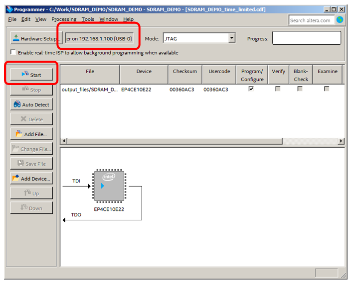
There is, of course, a similar path that goes through the GUI interface, but it’s more logical to do everything in batch. Therefore, I described a batch version. When all these theses have been completed (and the system administrators have completed them), we launch the programmer on our machine, we see a message about the lack of equipment. Click Hardware Setup:
Go to the JTAG Settings tab and click Add Server:
Enter the network address of Redd (I have 192.168.1.100) and password:
Make sure the connection is successful.
I spent three May holidays to achieve this, and then administrators decided everything.
Switch to the Hardware Settings tab, open the drop-down list and select the remote programmer there:
That's it, now you can use it. The Start button is unlocked.
The first "firmware"
Well. For the article to have real practical value, let's analyze the simplest “firmware” made using the above methods. The simplest thing that I really managed to implement for the complex is a test of the SDRAM chip. Here on this example and practice.
There are a number of amateur cores to support SDRAM, but they all turn on somehow tricky. And accounting for all the tricks is labor. We will try to use ready-made solutions that can be inserted into the NIOS II computing system, so we will use the standard SDRAM Controller Core. The core itself is described in the Embedded Peripherals IP User Guide., and a lot of space in the description is devoted to the clock shift for SDRAM relative to the core clock. Complex theoretical calculations and formulas are given, but what to do is not particularly reported. What to do can be found in the document Using the SDRAM on Altera's DE0 Board with Verilog Designs . In the course of the analysis, I will apply the knowledge from this document.
I will be developing in the free version of Quartus Prime 17.0. I focus on this, since during the assembly, they tell me that in the future, the core of the SDRAM Controllerwill be kicked out of the free version. If this has already happened in your development environment, no one bothers to download the free 17th version and install it on a virtual machine. The main work is done wherever you are used to, and the firmware for Redd with SDRAM is in the 17th version. Well, that’s if you use the free options. Nobody threatened to throw it out of paid ones yet. But I was distracted. Create a new project:
Call it SDRAM_DEMO. The name should be remembered: I'm going to carry out superfast development, so the processor system itself should be at the top level, without any Verilog-layers. And for this to happen, the name of the processor system must match the name of the project. So remember it.
Agreeing with the default values in a few steps, we come to the choice of a crystal. We select the EP4CE10E22C7 used in the complex.
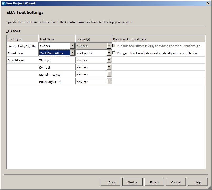
In the next step, out of habit, I choose modeling in ModelSim-Altera. Today we will not model anything, but everything can come in handy. It is better to develop such a habit and follow it:
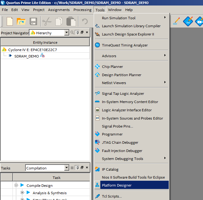
The project is created. Immediately go to the creation of the processor system (Tools-> Platform Designer):
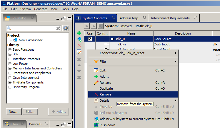
We created a system containing a clock and reset module:
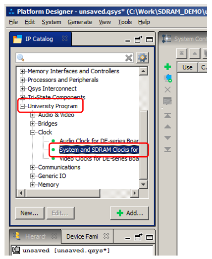
But as I mentioned, a special clock is required for the SDRAM kernel. Therefore, the standard module is ruthlessly thrown out
And instead of it we add the University Program-> System and SDRAM Clock for DE-series boards block:
In the properties, select DE0-Nano, as the inspiration for the SDRAM switching circuit was drawn from this breadboard:
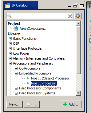
We begin to fill our processor system. Of course, the first thing to add to it is the processor core itself. Let it be Processor And Peripherals-> Embedded Processors-> NIOS II Processor.
For him, we do not fill out any properties yet. Just click Finish, even though we have formed a series of error messages. So far, there is no equipment that will eliminate these errors.
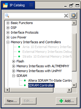
Now add the actual SDRAM. Memory Interfaces and Controllers-> SDRAM-> SDRAM Controller.
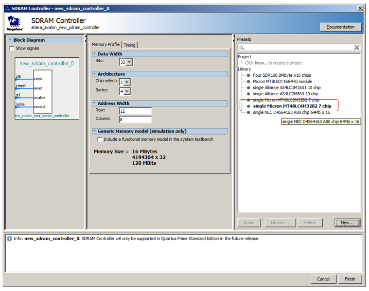
Here we have to hold on to filling out the properties. Select the nearest microcircuit similar in organization from the list and click Apppy. Its properties fall into the fields Memory Profile:
Now we change the bit width of the data bus by 16, the number of address lines - by 13, and the columns - by 9.
I still do not correct the times, perhaps in the future this recommendation will be changed.
The processor system implies a program. The program must be stored somewhere. We will test the SDRAM chip. At the moment, we cannot trust her. Therefore, to store the program, add memory based on block RAM FPGA. Basic Functions-> On Chip Memory-> On-Chip Memory (RAM or ROM):
Volume ... Well, let it be 32 kilobytes.
This memory must be loading from somewhere. For this to happen, check the Enable non-default initialization file box and enter some meaningful file name. Let's say firmware.hex:
The article is already complicated, so we won’t overload it. We will simply output the physical result of the test in the form of PASS / FAIL lines (and we will see the logical result with my favorite JTAG debugging). To do this, add the GPIO port. Processors and Peripherals-> Peripherals-> PIO (Parallel IO):
Set 2 bits in the properties, I also like to check the box for individual bit control. Also just a habit.
We got such a system with a bunch of errors:
We begin to eliminate them. To begin with, we will break the clock and reset. At the clock and reset unit, the inputs must be thrown out. To do this, there are fields that say "Double-click to export":
Click, but give more or less short names.
You also need to throw out the SDRAM clock output:
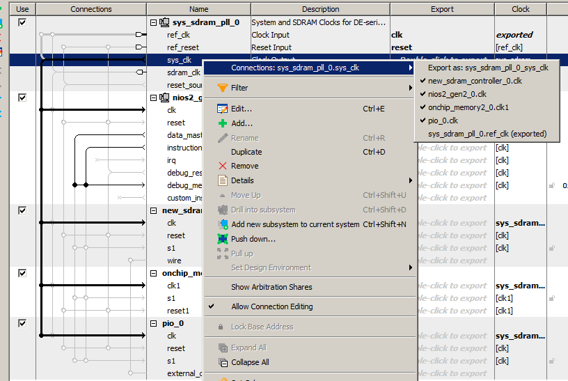
Now we split sys_clk to all clock inputs, and reset_source to all reset lines. You can gently hit the points connecting the corresponding lines with the “mouse”, or you can go to the corresponding exit, click the right mouse button, and then go to the Connections submenu in the drop-down menu and select the connections there.
Then we connect the tires together. We connect Data Master to all buses of all devices, and Inctruction Master - to almost all. It is not required to connect it to the PIO_0 bus. From there, instructions will definitely not be read.
Now you can resolve address conflicts. To do this, select the menu item System-> Assign Base Addresses:
And when we got addresses, we can also assign vectors. To do this, go to the properties of the processor core (point to it, press the right mouse button and select the Edit menu item) and configure the vectors on Onchip Memory there. Just select this type of memory in the drop-down lists, the numbers will be substituted themselves.
No errors left. But two warnings remain. I forgot to export the SDRAM and PIO lines.
As we already did this for the reset and clock block, double-click on the required legs and give them the shortest (but understandable) names:
Everything, there are no more errors or warnings. Save the system. Moreover, the name must coincide with the name of the project, so that the processor system becomes an element of the top level in the project. Have not forgotten what we called it?
Well, we press the most important button - generate HDL.
Everything, the processor part is created. Click Finish. We are reminded that it would be nice to add this processor system to the project:
Add:
And there, using the Add button, we achieve the following picture: A
SIP file has not yet been created. Yes, and we do not need it in the framework of this article.
Uhhhh The first step has been taken. We draft the project so that the system finds out the project hierarchy and the legs used. Compilation errors are not scary. Just in the free version of the environment, kernels were created that work only while the JTAG adapter is connected. But in the Redd complex, it is always connected, as it is divorced on a common board, that is, we have nothing to fear. So we ignore these errors.
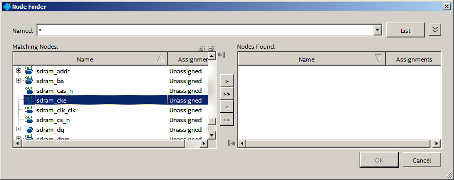
Now back to the description of the SDRAM kernel. It says that the CKE line is not used and is always connected to the unit. In fact, within the framework of the complex, FPGA legs are not just expensive, but a precious resource. And it would be foolish to spread the leg, which is always in the unit (and on the DE0-NANO board it is also not divorced). There would be a Verilog-layer, the corresponding chain could be cut there, but I save time (nervous laughter, looking at the volume of the already obtained document, but without saving it would have turned out even more). Therefore, there is no layer. How to be Go to the Assignment Editor. It is in it, since in Pin Planner, judging by the descriptions, there is no similar functionality.
There is still no line. Good. Create a new one.
Select the following icon:
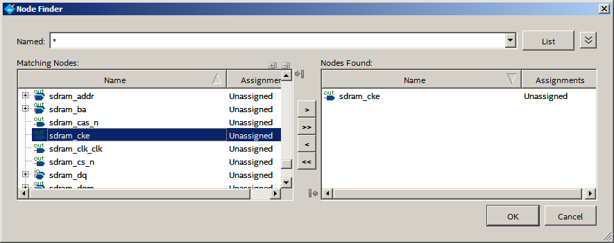
In the search system we set, click List and in the search results we find our CKE:
Add it to the right column, click OK.
We
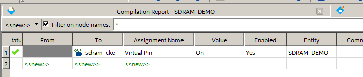
get the following list: In the yellow field, click on the drop-down list and find Virtual Pin. We choose. Yellowness moved to another cell:
There we choose On:
That's it, yellowness is gone. And the chain is now marked as virtual, which means that it does not require a physical leg. Therefore, we can not assign it to the physical conclusion of the FPGA. Close the Assignment Editor, open the Pin Planner. You can assign the legs, referring to the figure, or you can take the list from the * .qsf file, which is part of the project, which I will attach to the article.
That's it, close Pin Planner, we carry out the final compilation of the project. The hardware is ready, we proceed to the development of the software for the resulting processor system. But the article turned out so huge that we will do it next time .