Begin to study microcontrollers on the example of STM32F030f4p6
- From the sandbox
- Tutorial
0. Before reading the article
This article has the following objectives:
- show how to work specifically with this board;
- show the approach with which you can write a program flashing LED, relying solely on the documentation and logic;
- present the material in a language understandable to a person poorly familiar with microcontrollers.
The code will turn out to be minimalist from the point of view of using additional files - we will not include any file, except for those that are needed to build an empty, but valid, firmware. Those. based on the firmware code that works, but does not do anything useful.
We will need the following documentation:
- Datasheet STM32F030x4 (I use the document from January 2017 DocID024849 Rev 3);
- RM0360 Reference manual STM32F030x4 / x6 / x8 / xC (I use the document from April 2017 DocID025023 Rev 4);
- circuit board.
You can download these documents from the cloud .
The timer in the article will not be considered and will not be involved in the code.
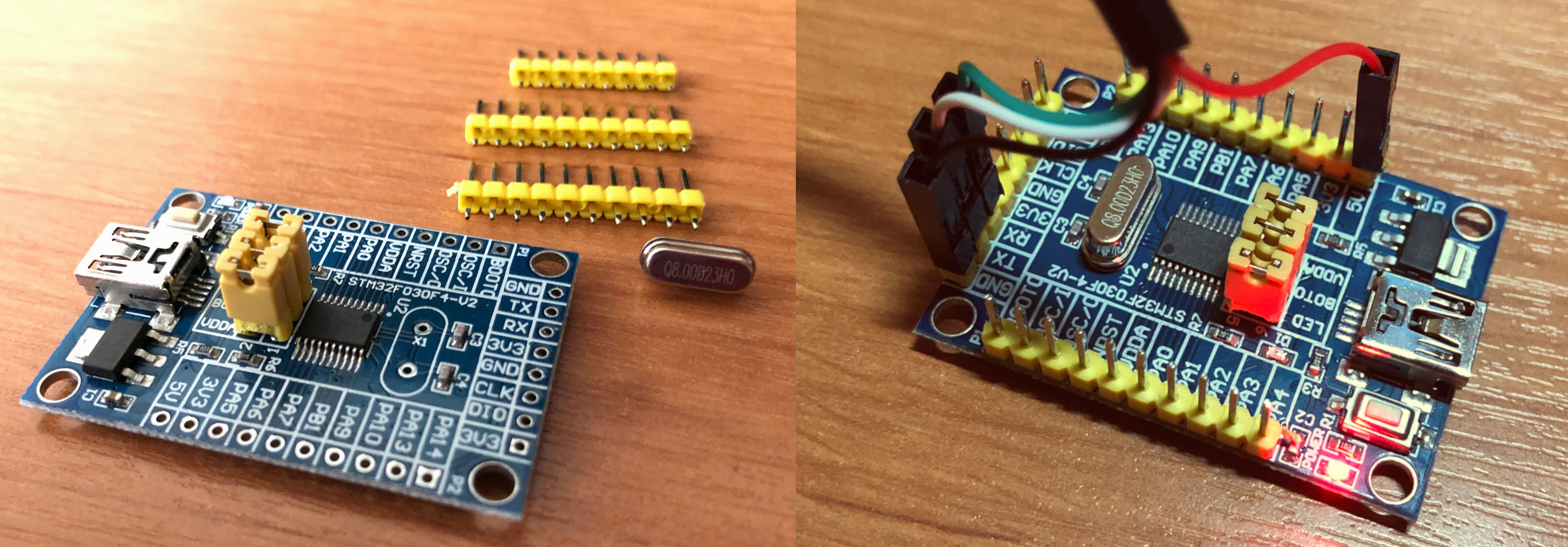
The ST-LINK programmer was not used. A USB-COM adapter (RS232 based on PL2303HX) was used to work with the board, which emulates a COM port.
Photo adapter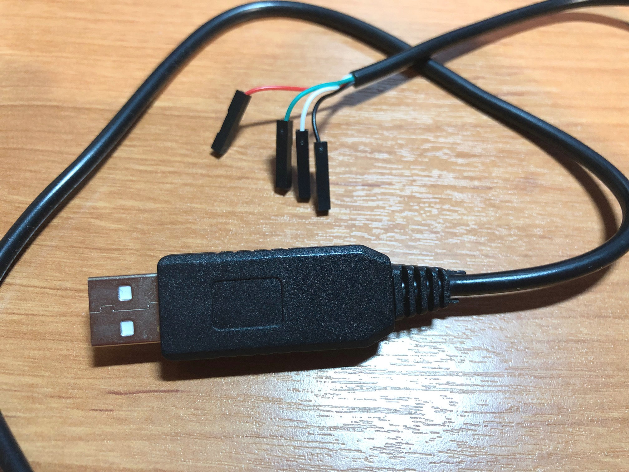
Everything was going on a Windows XP Professional 2002 SP3 virtual machine running through VirtualBox version 5.2.22r126460 on a Windows X host.
1. Installing the driver for the USB-COM adapter
Windows does not help, download from the Prolific website (the first link to the “prolific driver” request in Google) is a USB to UART / Serial / Printer PL2303 Windows Driver driver (we need the one that is Standard Driver ). Or you can download from my cloud .
Install the driver, reboot and see the new COM port.
Screenshot with the name of the installer and the new COM port
Port settings left standard. You can change the COM port number at your discretion. In my experience, only once in my life I saw that the program saw only the first 4 COM ports, if I am not mistaken, it was some kind of Bluetooth terminal under Windows.
COM port settings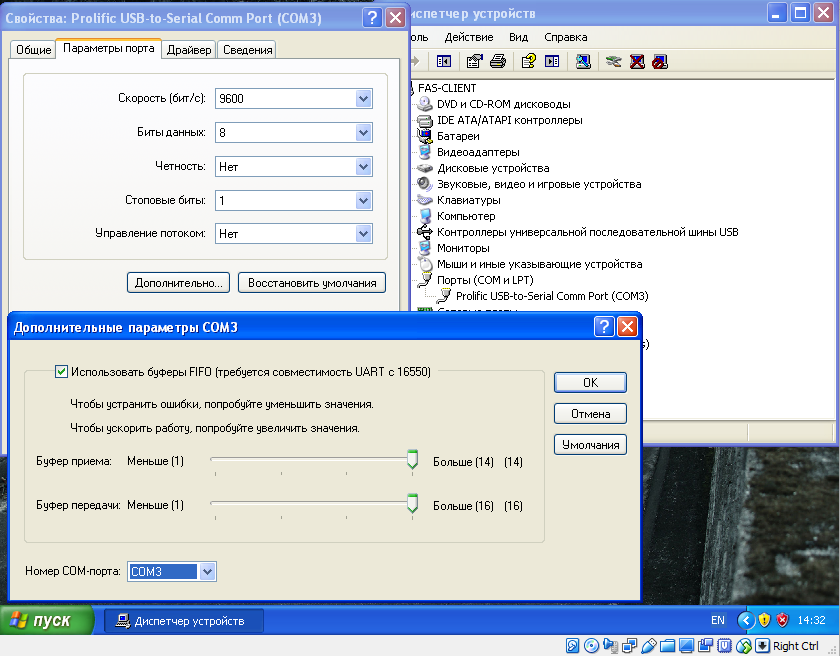
2. Fill firmware to and from the board
2.0 Downloading the utility for working with the board
We download FLASHER-STM32 utility (of STM32 Flash loader demonstrator (UM0462) in the description) from the off-site STM , for this we will have to register, but this is not terrible - as a result, we will drop the zip-archive with the installer; Next-> Next-> Next ... and everything is set. For convenience, I create a shortcut to this application in the working folder.
Here is this utility (screenshot of the site)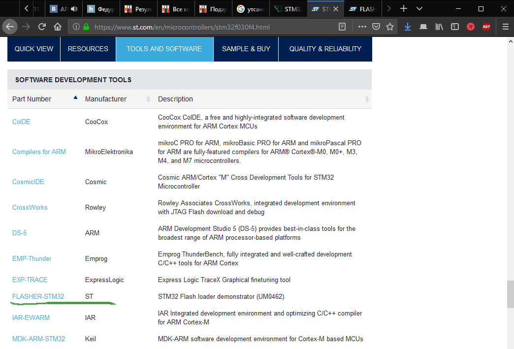
By default, the path to the C: Program Files \ STMicroelectronics \ Software \ Flash Loader Demo \ STMFlashLoader Demo.exe utility .
2.1 BOOT-nuance
The board has a jumper (jumper) BOOT.
- When the jumper is closed , the microcontroller will load instructions from its memory (that is, a program written by the programmer).
- When the jumper is open , the microcontroller will receive information along the RX and TX lines, i.e. will be stitched from the COM port (from the adapter in my case).
2.2 Configuring the utility
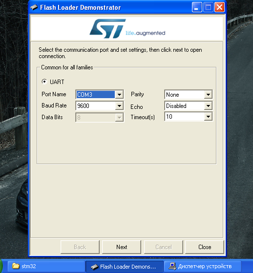
Run this application, it is actually the simplest (contains a minimum of settings). On the first window, select:
- interface (I have it COM-3);
- the speed with which the computer and the microcontroller will communicate (IMHO, 9600 is the normal value);
- the number of data bits (for some reason this window is not available to me, but so far it does not matter);
- parity (I have no parity, i.e. None);
- echo (I have OFF);
- waiting time (I have 10 seconds).
Click Next, and if everything is in order, then we will see a green light and “Target is readable”; if we see a red light, the computer could not connect.
Target is readable if the microcontroller is successfully determined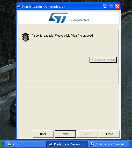
The order of steps that always help:
- First, you need to check if the BOOT jumper is closed on the board.
- Secondly, in any case, turn off the power of the microcontroller and preferably the TX and RX lines going from the adapter to the board (the ground can not be disconnected).
- Thirdly, in the program to press Back to the end, i.e. before the first page, or even close it and restart it (generally speaking, it sometimes hangs). It is important to always start from the first page before each connection to the board through this program.
- Fourth, pick up the wires from the adapter to the board and try again to connect to the program (always from the first page!).
If all else fails, you can try to disable everything, restart the computer, and try to reconnect to the board.
Because I work through a virtual machine, I have to reconnect the USB-COM adapter several times so that it is detected by the virtual machine and the host machine does not have time to install non-working drivers.
Another option that I found working at the time of writing this article is to press a button on the board instead of constantly jerking the wires. However, the BOOT jumper will be closed and opened in any case. This option works, because the button is connected to the foot of the external reset NRST .
On the next window, select the target device Target. By the way, sometimes you can see (perhaps this is a bug) in general, the left device, for example instead of STM32, see STM8 - somewhere there was some kind of failure, the order of treatment is described above. Therefore, in this step, you can not hurry to press Next, but always pay attention to the fact that the desired device is selected in Target.
Target Device Selection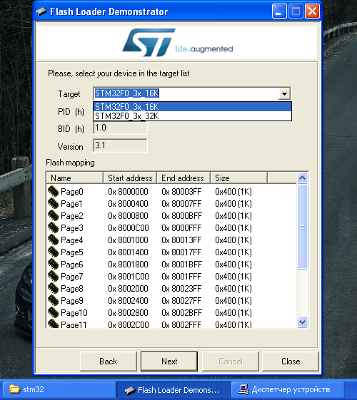
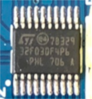
How to determine what our device? - we look at the chip and rewrite everything we have written on it. Open the Datasheet on our chip, in the Ordering information section it is described which letter is responsible for what. In my case it is:
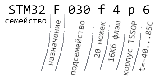
I choose my chip (16K) in Target and move on.
There are a choice of 4 actions with a chip:
- erase memory (whole or select a specific area);
- write firmware to the device;
- read the firmware from the device;
- enable / disable write protect or read protection.
2.3 Read firmware from board
At the very first connection of my board, I decided to keep the original firmware, a sort of backup - we will do it now. You will need to specify where to save this firmware and which memory pages to save, you can also choose to use the hex , bin or s19 file format.
Select memory pages to read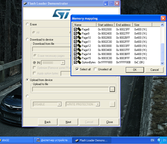
If you only upload to the board or read firmware from the board, then there is no difference between these file formats. Next comes the progress page, where I sometimes hang up the process for 99% for a long time (not necessarily exactly 99), but after a few seconds it supposedly successfully completes - in fact, after that, the board did not show the behavior that would correspond to the loaded firmware. Simply put, you need to reconnect everything and re-fill the firmware, nothing critical in this.
The firmware file is preserved, and in the future it can be uploaded to the board.
However, if read protection is installed, the firmware will not work.
Progress window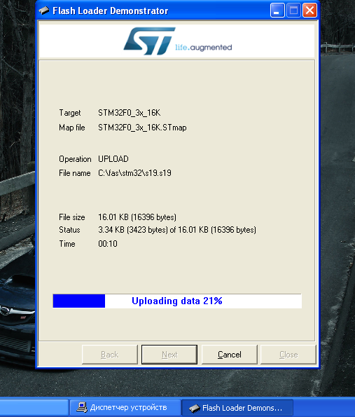
2.4 Flashing the board
Now we will upload the firmware file, the writing of the source code of which is given below. Looking ahead, I’ll say that we’ll upload bin and hex files, because they will be given out by the development environment. Additional settings for s19 and hex files are identical; Unlike them, in the bin file, you can choose the address from which the firmware will be recorded, by default in the utility it is equal to 8000000 (it suits us).
Preparing to record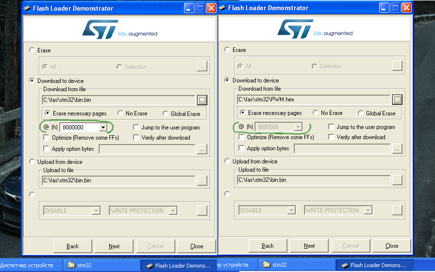
Before recording, you can clear the microcontroller's flash memory by selecting one of three options:
- Erase necessary pages;
- No Erase (without cleaning);
- Global Erase (full cleaning).
In fact, cleaning is the process of writing zeros to memory.
There are still optional bytes, but for now you can leave them alone. Click Next, wait for the completion of the process and everything is ready.
In case you want to write down my firmware, you can find it in the cloud, the file blink.bin . When using this firmware, the built-in LED powered by the PA4 leg should flash.
3. Writing code
3.0 Installing CooCox CoIDE Development Environment
The IDE can be downloaded from the SoftPedia.com site , previously it was possible to download from the STM site and from the IDE site itself, but since the IDE was no longer supported, this has become impossible. There is nothing critical in the fact that the IDE stopped supporting, no, because for writing code, the main thing is the compiler. I downloaded both versions, but I use version 1.7.8.
The first launch of the environment is well described here , Next-> Next-> Next ... and nothing complicated. I will add only that first it is better to create a project, and then everything else.
And yet, if you lost the Repository tab, you can find it in the View -> Repository menu .
Download tools (compiler) for the environment hereor ask Google for “gnu tools for arm”; I downloaded the option that has sha1.exe at the end.
3.1 Source Framework
So, the project has been created, the chip has been selected, now we will add to the project a minimal set of sources, without which it cannot live at all.
This is how a project should look like when it is first created, i.e. there is only the main file main.c and nothing more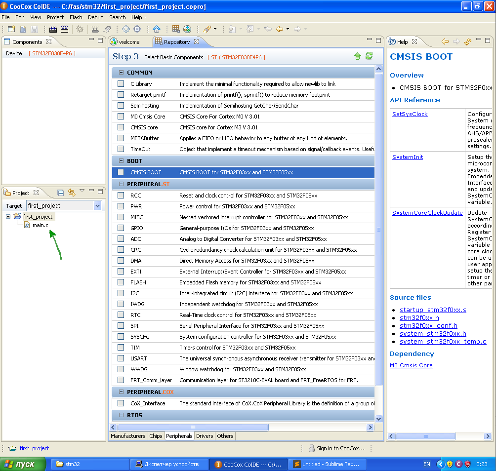
We distinguish CMSIS BOOT and Wednesday will automatically allocate the M0 Cmsis Core , as dependencies require it.
Now we get the minimum set of sources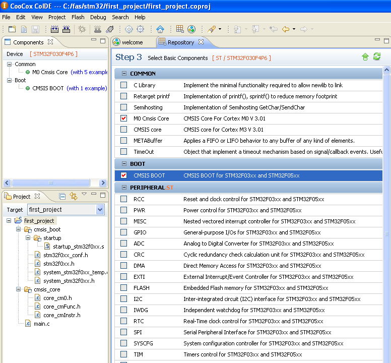
Build the project (Build icon, or F7 key). For reasons I do not understand, the hex file is not assembled (there is a warning in the console); I reinstalled the IDE and the compiler several times, re-created the project, but for some reason this result was on the virtual machine; on another computer (not virtual, but real) everything is one-to-one and the output is a working hex. Fortunately, there is a bin.
Project successfully assembled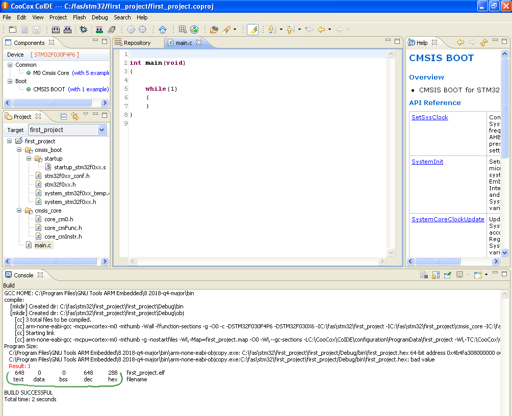
I advise you to pay attention to the file size, you can see it at the end of the output in the console, or you can see it with standard tools (here, by the way, you can see that hex is empty); At the same time on this screenshot you can see that the firmware files are in the project folder, then Debug / bin /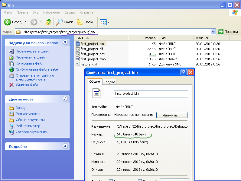
Although the code does not do anything, I upload it to the board in order to make sure that it is possible to fill in (which, for example, the utility does not discard). I advise you to do this and the reader. If it fails, try again and again, and write comments.
3.2 Finger algorithm
To begin with we will outline algorithm as from the point of view of the person the microcontroller will blink a LED. And for this, a little reasoning.
Each equipment works at the expense of stored energy, for example, some engines can operate on different types of fuel, but for this purpose the engine needs to be adjusted to the type of fuel we are going to feed it with. Similarly, the microcontroller needs to be adjusted (customized) for an energy source - this will be the first block of the algorithm.
We reason further. The desktop computer has a monitor, speakers, keyboard, mouse ... and you can see that some devices provide us with information, and with the help of others we provide information to the computer, but they are all connected to a common box for all of them (the system unit). You can guess that the microcontroller can receive and give information, which means that its legs can receive a signal or give a signal - this will be the next block of the algorithm.
Next, the microcontroller should turn on the LED, wait for some time, turn off the LED, wait for some time and re-enable-wait-turn off ...
As a result, the algorithm will look something like this
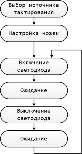
The purpose of this flowchart is to visually show what the algorithm is doing; First of all, the scheme is written for itself, so everyone is free to write / draw it as he wants (for himself). I believe that the scheme should aim to be as simple as possible, readable and visual, and have a high level of abstraction.
In accordance with this algorithm, we will write code.
3.3 Work with documentation
I recommend reading this part of the article with the open file stm32f0xx.h , which lies in the cmsis_boot folder of our project, and open documentation.
3.3.1 Choice of clock source
First, you need to provide power to the microcontroller. The microcontroller receives from the adapter 5 volts (measured with a multimeter), but the question arises “at what frequency does the microcontroller work”, because it is known that the electronics operate at different frequencies. First open the datasheet , in the content you can see two sections that are relevant in meaning: Power management , Clocks and startup . The first one deals with voltage and low-power modes. The second section hides what we are interested in at the moment. Already in the very first sentence it says "the internal RC 8 MHz oscillator is selected as default CPU clock on reset", which means thatBy default, after resetting the MC, the internal 8-MHz RC-chain is selected as the main clock source .
Next is some kind of incomprehensible Clock Tree scheme, which we will look at later.
Clock tree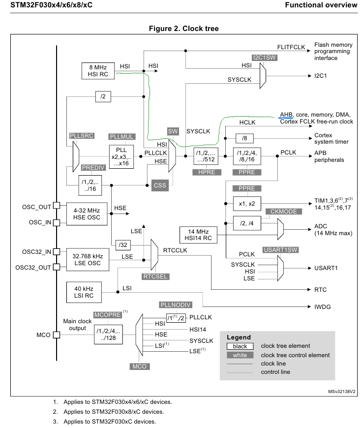
Strictly speaking, you can rely on the phrase “by default after resetting the MC ...” and read this part of the article diagonally.
Now you need to be distracted by the board and look for the internal LED. I know that the diodes on the circuits are designated D1 , D2 ..., i.e. D == diode , on my board near the resistor R7 is a diode D1 .
Photo board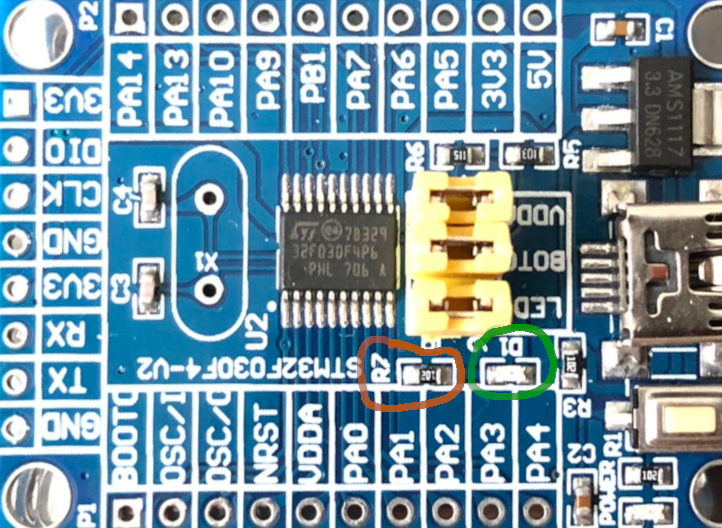
Perhaps, having carefully examined the board, you will be able to trace to which leg the diode is attached, but I will turn to the circuit board. Unfortunately, the elements of the board do not exactly correspond to the elements on the diagram in their location; but I am glad that I found such a scheme on the Internet (otherwise I could not find anything for a long time).
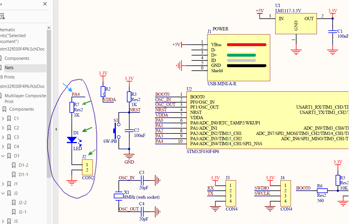
In the diagram we can see that the cathode of the diode through jumper J2 is hooked up to the ground, and the anode through the resistor is hooked up to the output PA4 . PA4 means the 4th pin of port A , which means that in order to turn on and off the LED, you will have to apply voltage to the pin PA4 .
Next, you need to determine how to apply voltage to this pin. For me, it was not at all intuitive, and I plowed documentation for a long time along and across until I came across the datasheet at the very beginning of the block diagram diagram in the Description section . And in it, I saw the cherished PA track [15: 0] <=> GPIO port A <=> AHB decoder <=> Bus matrix <=> Cortex-M0 , i.e. Port A is a general-purpose I / O port and is connected to the AHB bus .
Block diagram
(The picture is clickable)
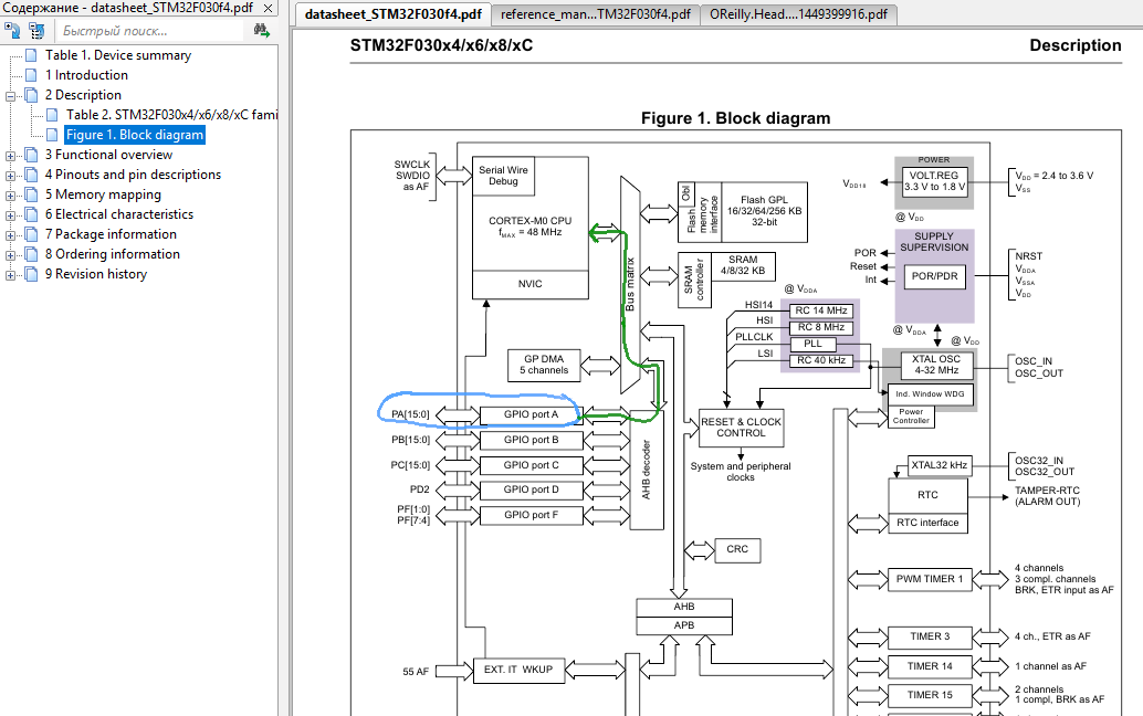
I note that in electronics it is customary to break the microcontroller pins into ports, and usually the port has 16 pins. The diagram shows that ports A , B and C have just 16 of them, but ports D and F have fewer of them (less than 16 pins maybe more, no).
Let's go back to the Clock tree scheme and find the output signed by AHB . Let's figure out what frequency this output works. The AHB signal goes HCLK , which comes out of the HPRE divider . This divider receives a SYSCLK signal from the SW switch. It is programmatically specified which of the signals at the SW input will be used as SYSCLK - then we will set this in the code. You can choose from:
- HSI - a signal from an internal high-frequency generator, it is output by an 8 MHz crystal resonator, which I soldered before working with this board;
- PLLCLK - signal from the frequency multiplier PLLMUL ;
- HSE - signal from an external high-frequency generator.
Any option is suitable for our task, I suggest choosing the simplest and most accessible of them - HSI .
Let's go to the Reference manual and open section 7 Reset and clock control (RCC) , and specifically 7.2.6 System clock selection , where we again come across a similar wording found in the datasheet: “after a system reset, the HSI oscillator is selected as system clock ”- i.e. we don’t even need to do anything, MK will start himself on HSI .
To make sure that the MC really will work from this source, I will state it explicitly in the program; we scroll to the registers that are responsible for the reset and clocking (section 7.4 of the RCC registers). The first register described in the documentation is Clock control register (RCC_CR) ; Below is a description of the bits, which is responsible for what.
Clock Control Register
We are interested in the zero bit of HSION , which is responsible for turning on the resonator ( 0 is off, 1 is on).
Thus, it will be necessary to write the unit to the RCC_CR register . (zero bit is one, or 2 0 = 1).
Now in the stm32f0xx.h file we find the definition of RCC ( # define RCC ).
RCC-> RC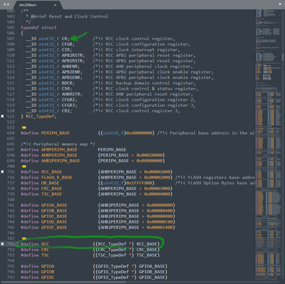
As you can see, this is a structure located at RCC_BASE ; address 0x40021000 , if you expand all define , the same address can be seen in the Reference manual in section 2.2.2 of the Memory Map and register boundary adresses and in the datasheet in section 5 of the Memory mapping ( AHB area ).
To write a unit in the CR register of the RCC block to enable HSI , you will need a line of code
RCC->CR |= 0x1;3.3.2 Foot adjustment
Signaling the microcontroller's foot to light up the LED and stopping the signal in order for the LED to go out are simple actions, and therefore it refers to GPIO functions (general-purpose I / O ports).
By default, the legs of the MC are not connected, i.e. output uncertainty. It is necessary to connect the port, the leg of which will power the LED. Earlier, we determined that the GPIO ports are connected to the AHB bus — you need to patch up this bus. Continuing to scroll through section 7.4 of the RCC registers (reset and control control registers), we encounter section 7.4.6 of the AHB peripheral clock enable register ( RCC_AHBENR , register of the closure of the AHB bus)). Previously, I have determined that my LED is connected to pin PA4 - accordingly I need to write unit in the 17th bit register to zataktirovat port A .
AHB peripheral clock enable register
Accordingly, the code must be
RCC->AHBENR |= (1 << 17);or, which is the same,
RCC->AHBENR |= 0x20000;either using stm32f0xx.h #define file to write
RCC->AHBENR |= RCC_AHBENR_GPIOAEN;RCC-> AHBENR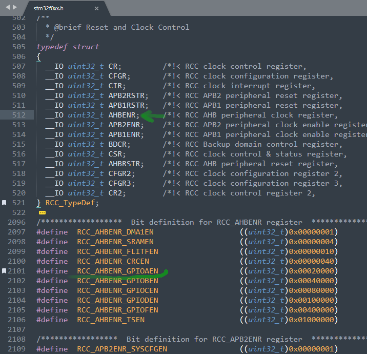
We powered up port A , now we need to inform MC that PA4 will work on the way out - we will read section 8 of the General-purpose I / Os (GPIO) ; In the introduction of the section, “Each general-purpose port has four 32-bit configuration registers ( GPIOx_MODER , GPIOx_OTYPER , GPIOx_OSPEEDR and GPIOx_PUPDR ), two 32-bit data registers ( GPIOx_IDR and GPIOx_ODR ) ...” - each GPIO the port has 4 tuning registers and 2 data registers - this is what we need (configure port A , or rather the output of PA4, and periodically send it 0 and 1 ). For a better understanding (theory) of what is happening, you can read this section, but I scroll down to section 8.4 of the GPIO registers and configure the port in accordance with the descriptions.
- port mode - exit. In accordance with the documentation, it is necessary to record 01 in the corresponding area ( MODER4 ) of the corresponding register ( GPIOA_MODER ), i.e. bits 9 and 8 : in the 9th bit should be zero, in the 8th unit:
GPIOA->MODER |= (1 << 8); // илиGPIOA->MODER |= 0x100; // илиGPIOA->MODER |= GPIO_MODER_MODER4_0;GPIO port mode register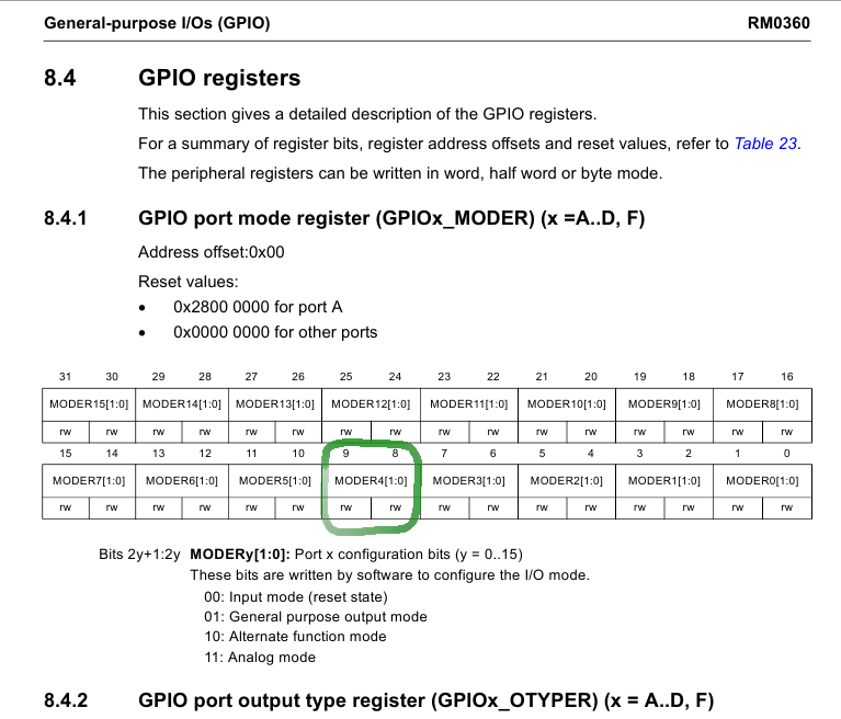 GPIOA-> MODER
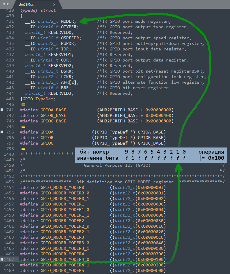
- type of output. Honestly, I still have not fully understood the circuit design of this case (I will understand, re-read forums, etc.), but studying other resources on the configuration of the MK output, as well as logic and intuition, suggest that there should be a push -pull and then should be pull-up . In any case, the code is written, everything works and nothing has burned. There is a real risk of burning if you select the open-drain type and short-circuit this output with another device, since This is an open exit and is not protected by anything. In addition, we have a current limiting resistor in front of the diode - here it certainly will not burn.
Following the documentation, it is necessary to write a zero in the 4th bit; the documentation also states that after a reset, there will be zero here.GPIOA->OTYPER &= ~(1 << 4); // илиGPIOA->OTYPER &= ~0x10; // илиGPIOA->OTYPER &= ~GPIO_OTYPER_OT_4;GPIO port output type register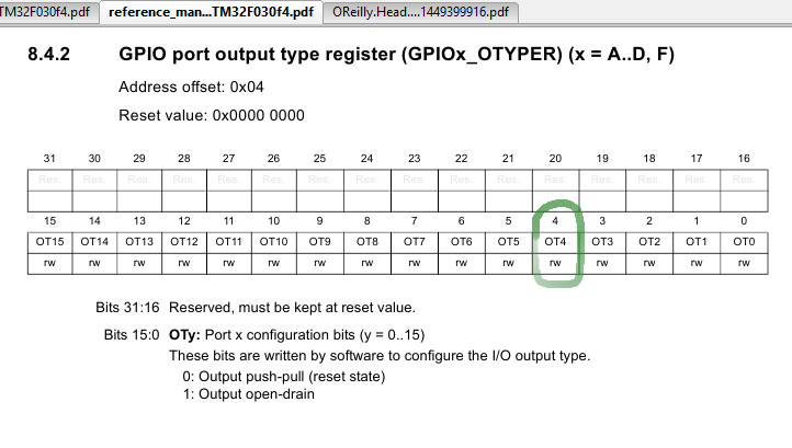
- output speed . In our case, it does not matter, but for fidelity, I will write here a zero.
GPIOA->OSPEEDR &= ~(1 << 8); // илиGPIOA->OSPEEDR &= ~0x100; // илиGPIOA->OSPEEDR &= ~GPIO_OSPEEDER_OSPEEDR4_0;GPIO port output speed register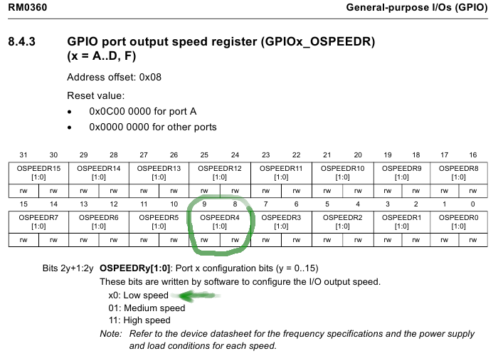
- lift . Because the output will power the LED, it is necessary to pull up to the power, i.e. pull-up .
It is necessary to tighten the 4th output of port A ; the documentation says that for this it is necessary to write zero and one bits in 9 and 8, respectively.GPIOA->PUPDR |= (1 << 8); // илиGPIOA->PUPDR |= 0x100; // илиGPIOA->PUPDR |= GPIO_PUPDR_PUPDR4_0;GPIO port pull-up / pull-down register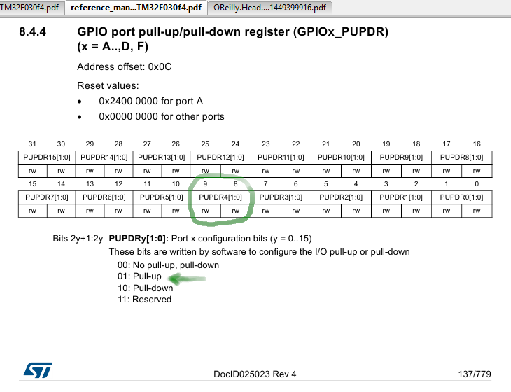 GPIOA-> PUPDR
3.3.3 LED on-off and delay
Earlier we read that each port has registers, including the IDR and ODR data registers - the input and output registers, respectively. Logical zeros and ones on the MK leg - is this data? - yes, data. Data can come into the microcontroller from the outside (to be input ) and exit from the microcontroller and go to another device (to be output ). The unit on the MK leg is the presence of a high voltage level, i.e. If you output the unit to the output, then there will be a voltage, and this voltage can power our LED. Outputting a unit to a microcontroller's leg is something else than writing this unit to the ODR output register .
GPIO port output data register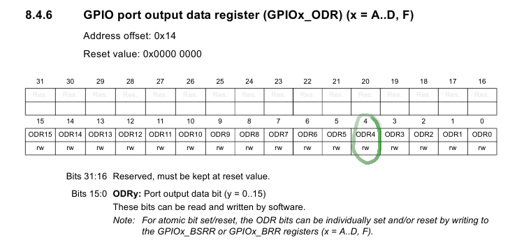
According to the documentation, we see that for each port ( A , B , C , D , F ) there is a 32-bit register, however, since since a port cannot have more than 16 pins, only the first 16 bits of the register are used. Each bit corresponds to the port number (output). To output the unit on the PA4 pin, you need to write down the unit to the 4th bit, to output a zero — write zero to the 4th bit, i.e. remove the voltage from the output.

GPIOA-> ODR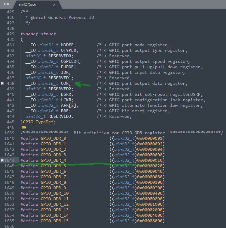
The code to turn on the LED will look like this
GPIOA->ODR |= (1 << 4); // илиGPIOA->ODR |= 0x10; // илиGPIOA->ODR |= GPIO_ODR_4;Code to turn off the LED
GPIOA->ODR &= ~(1 << 4); // илиGPIOA->ODR &= ~0x10; // илиGPIOA->ODR &= ~GPIO_ODR_4;But if you write the line for turning off the LED after the line for turning on, then the LED will not blink (if you are wondering what will happen - you can try; it will not burn anything, it has already been discussed above) - it means you need to make a delay. For the delay, timers are used, but the timers are worthy of a separate article (due to the complexity), so we will make a crutch delay: we will drive the idle cycle. There is one thing: if compiler optimization is enabled , the compiler will cut out our idle cycle, and there will be no delay. Make sure that optimization is not enabled. To do this, go to the project configuration (right-click on the project name in the project tree) and check the string Compile Control String in the Compile tab : it should have an argument-O0 (“o zero” means that optimization is disabled). If you collected everything according to my instructions, then most likely you will also have -O0 , since This was the default and I did not touch anything here. Arguments -O1 -O2 -O3 means that the optimization of the corresponding level is enabled.
Compiler Optimization Check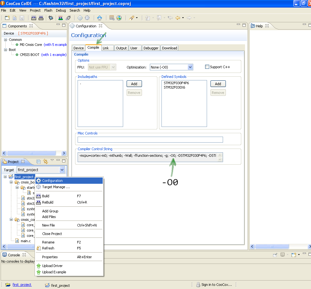
The idle cycle can be written like this:
    int t = 4000000;
    while(t > 0) t--;
I set the value of t to those by chance, argued as follows: if the microcontroller runs at 8MHz, then in a second it will execute an estimated 8,000,000 instructions; if it is deeply exaggerated, then for a half-second delay it will be necessary to drive the cycle 4,000,000 times.
The idle cycle will need to be chased after the LED is turned on, and after it is turned off, and together it will loop.
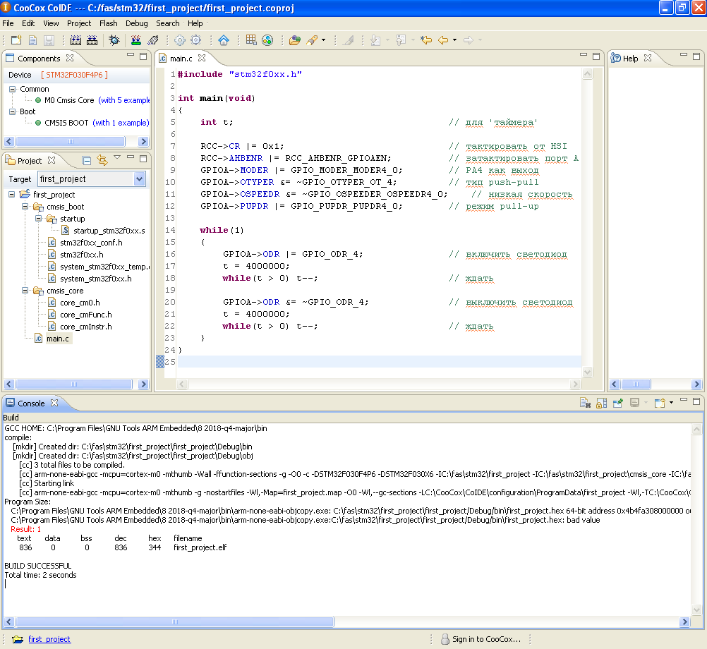
3.4 Writing code and running
Putting together all the lines of code that we wrote before. You also need to include the header file stm32f0xx.h , because we relied on it and took from it the definitions of structures, addresses and values. The result should be:
#include "stm32f0xx.h"
int main(void)
{
    int t;                                       // для 'таймера'
    RCC->CR |= 0x1;                              // тактировать от HSI
    RCC->AHBENR |= RCC_AHBENR_GPIOAEN;           // затактировать порт A
    GPIOA->MODER |= GPIO_MODER_MODER4_0;         // PA4 как выход
    GPIOA->OTYPER &= ~GPIO_OTYPER_OT_4;          // тип push-pull для PA4
    GPIOA->OSPEEDR &= ~GPIO_OSPEEDER_OSPEEDR4_0;    // низкая скорость для PA4
    GPIOA->PUPDR |= GPIO_PUPDR_PUPDR4_0;         // режим pull-up для PA4
    while(1)
    {
        GPIOA->ODR |= GPIO_ODR_4;                // включить светодиод на PA4
        t = 4000000;
        while(t > 0) t--;                        // ждать
        GPIOA->ODR &= ~GPIO_ODR_4;               // выключить светодиод на PA4
        t = 4000000;
        while(t > 0) t--;                        // ждать
    }
}
We press Rebuild and fill in the code to the board through the utility.
In order for the board to launch a new firmware, do not forget to close the BOOT jumper and make a reset (RESET).
4. Conclusion
The code is written, everything works. Forces spent Nemer. I am glad that based on the documentation, it turned out to write a working code, largely due to the fact that STM has high-quality documentation.
There are plans to write an article on how to assemble everything with your hands, without an IDE, through the console, true oldschool , ideally so that you can do all this from under Linux. Now I am working on PWM and ADC (also on this board) - I'll write an article on them too.