The device of an IC chip with ball terminals and why the ball disconnects
We all love electronics and almost worship it. Phones, computers, etc. devices are very complex, and because they do not cost fabulous money, thanks to automation and CAD, but we still think that it is expensive, and we want cheaper, and we don’t even know how many technologies it contains microelectronics.
One of such hidden technologies for which we pay when buying a processor, phone, video card and other devices - UBM (under bump metallization) is the metallization of a platform on a chip for mounting ball leads.
The development of microelectronics leads to an increase in the density of integration of the components both on the IC chip and on the PCB. If there are not too many conclusions on the crystal, from one to a couple of hundreds or more, then the crystal can be designed for wire welding. There are many examples: flash memory, RAM chips, sound chips, and more. Here, the reader can recall how some of the microcircuit cases look, and say that the cases are soldered to the ball terminals, and he will be right. Only inside these cases are crystals glued and welded with wire. Next, we will talk about ball leads located between the crystal and the body.
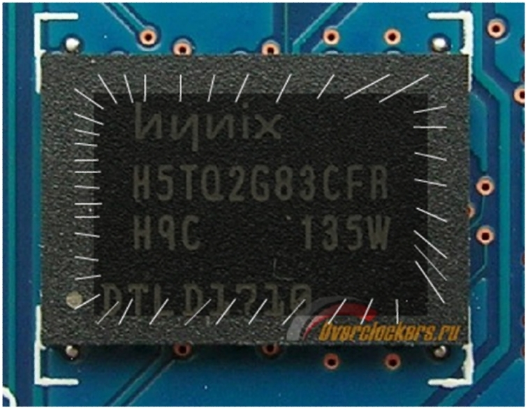
Fig. 1 Hunix RAM Chip. Crystal unpacking (white lines) and
the crystal itself (dark rectangle) are shown schematically , although the case itself is soldered on balls.
If the number of pins of a potential crystal is large, from 600 to over 4000, then the developer develops a crystal immediately for ball pins, for example, such crystals as CPU and GPU. Yes, and physically unzipping a wire with such a number of conclusions is a long sequential process, but I generally keep quiet about programming a machine.
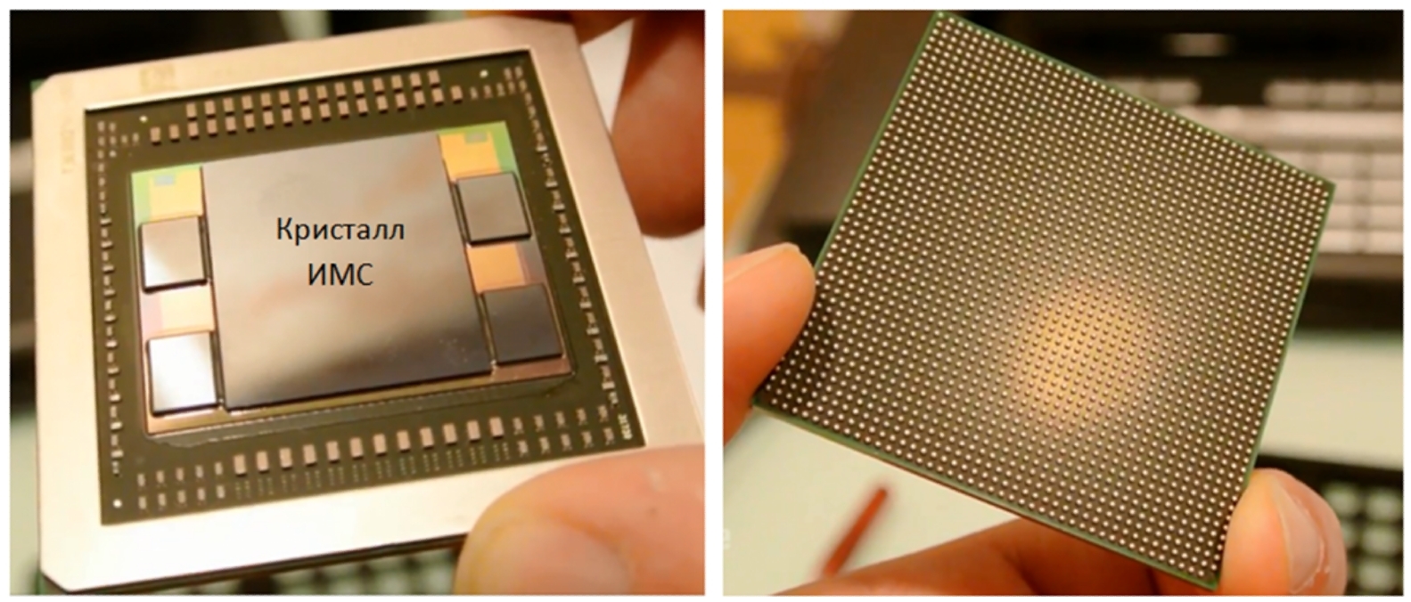
Fig. 2 AMD Fiji graphics chip. On the IC chip, more than 4000 solder balls, not on the body.
The ball lead is a ball of solder (it can be lead-containing or without it), which performs 3 functions at the same time:
1. Holds the crystal on a textolite or silicon interposer (like AMD Fiji)
2. Serves to remove heat
3. Creates an electrical connection of the crystal with the external environment
If the crystal is made for ball leads, then copper contact pads are formed over the entire surface of the crystal in the form of a matrix, and are essentially a continuation of the crystal topology. Then, on a copper, where necessary, a passivation protective layer is applied, and is not applied where the ball will be located. The open area of copper is covered with a UBM layer and after that it is ready to apply the ball. Part of the UBM layer rests on passivation, thereby completely covering the copper and creating a protrusion around the perimeter of the site.
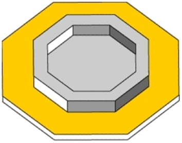
Fig. 3 KP under a ball conclusion. Yellow - copper under passivation, gray - UBM coating.
If the crystal is made for wire welding, then the contact pads (KP) for welding are rectangles with a coating mainly of aluminum, and are located around the perimeter of the crystal.
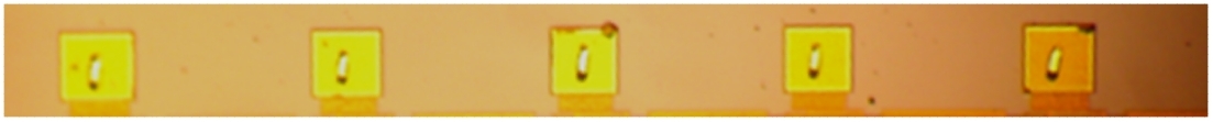 Fig. 4 KP for wire welding with a size of the order of 100 x 100 microns
It is also impossible to directly connect a solder ball to such a KP: solder cannot be soldered to an aluminum pad. To do this, solder the ball, also use UBM technology.
And so, UBM is the layer between the solder ball and the metal of the contact pad on the chip. Its task is adhesion with a contact pad, diffusion protection and wettability for solder. UBM is needed to create structures with ball joints and it also allows you to create structures for balls and on ICs created for splicing.
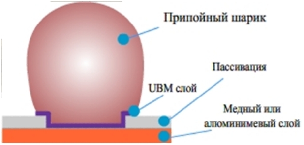
Fig. 5 Location of the UBM
The UBM interface must ensure that the following conditions are met:
1. Create a reliable connection with the aluminum of the contact pad and with the passivation layer on the chip. It is important that the passivation layer itself be without small holes, because this can lead to a short circuit when creating conductive UBM layers.
2. Have a low resistance with a contact pad. To fulfill this requirement, alumina is removed from the surface of the CP before applying the first UBM layer.
3. Provide a barrier to the diffusion of the solder ball material and the KP material.
4. The outer layer of UBM must be wettable for solder.
5. Protect against the formation of an oxide layer on an open surface.
6. Provide as little voltage to the crystal as possible.
UBM is a minimum of 3 etched layers of thin metal films.
1. A layer of adhesion to the KP. It serves to form a bond between the metal of the KP and the passivation layer of the IC and protects against diffusion between the KP and the solder ball. Commonly used materials for this are: Chrome (Cr), titanium (Ti), titanium / tungsten (Ti / W), nickel (Ni), Mo molybdenum. The thickness of this layer is about 0.15 - 0.2 μm.
2. A layer wetted for solder. To create a solder joint with a solder ball. The metals used are: Copper (Cu), Nickel (Ni), Palladium (Pd). The usual layer thickness is ~ 1 - 5 μm.
3. Layer of protection against oxidation. For this, gold (Au) is used. Thickness ~ 0.05 - 0.1 μm.
You can make many combinations of UBM layers, for example, Ti / Cu / Au, Ti / Cu, Ti / Cu / Ni, TiW / Cu / Au, Cr / Cu / Au, Ni / Au, Ti / Ni / Pd, Mo / Pd . However, different UBM structures have different properties and different reliability. For example, Ti / Cu / Ni has better adhesion than Ti / Cu. Combinations of materials UBM affect the reliability of the connection to the site of the crystal, and to the ball of solder. UBM must be compatible with solder ball material. The outer layer of UBM, which works well with lead solders, may not be suitable for lead-free solders. For example, Cu gives a good solder compound with lead solders, and bad with lead-free ones, because pure tin forms an intermetallic compound with copper Sn-Cu. If the copper is completely absorbed by the solder, then the contact will break.
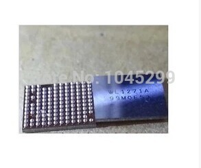
Let's see how it looks on the example of a microcircuit, which was originally developed for wire welding, and then finalized for ball outputs. Moreover, the topology of the crystal did not change for the balls. Indeed, if the crystal works, why climb? This is the WL1271L chip - Texas Instruments Wi-Fi and Bluetooth chip. In the photo, a fragment of it:
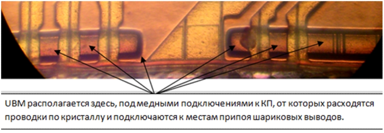
Fig. 6 Fragment of a crystal WL1271L.
Here, the moment attracts the attention that there is the possibility, without resorting to changing the topology of the crystal, to adapt it to the ball leads by forming layers on top of the crystal. This requires additional operations on the plate with crystals, the operation of forming balls, but this gives an advantage in saving space on the board, because with a ball size of 200 - 250 μm, it does not need an adapter board, that is, you can mount the crystal directly on the board. As far as I know, they do not do this in Russia, although there are microcircuits that are suitable for this, but some imported ICs do this. In a good way, such a technology should reduce the cost of the final product. For the military, it may not be suitable because of the requirements of reliability, but for home use, at an affordable price, it’s quite.
Now let's look at an example of an IC, which is designed specifically for ball terminals. We take a video card, and we crack the crystal, we clean it, we pickle it with a mixture of ammonium persulfate and copper sulfate.
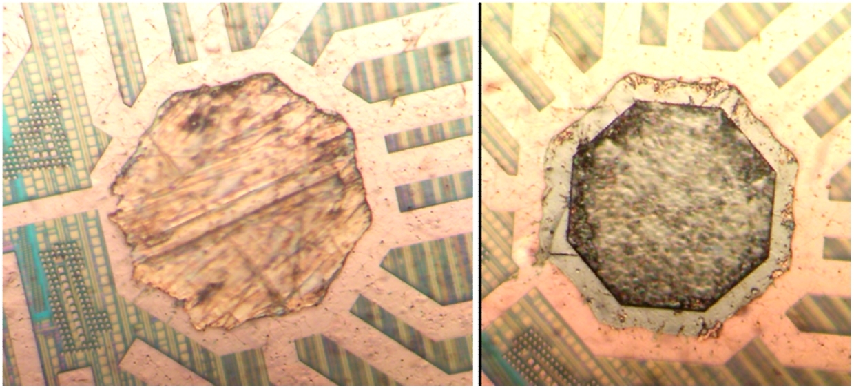
Fig. 7 Contact pad before (left) and after etching (right).
When tin is etched (and the balls must be leadless), tin displaces copper from copper sulfate, and then this copper in the form of metal is absorbed by ammonium persulfate. Thus, the site is cleared of tin. Under the microscope, when the focus changes, a depression is visible after the tin is removed, this is not so clearly visible in the photo. Copper wires diverging from the contact pad were not etched because they are protected by passivation. The copper under the contact pad itself also remained untouched, because the upper layer of UBM did not react with either ammonium persulfate or sulfate, thereby exposing itself and by this property it is possible to guess what kind of metal it is.
Now about the problem of ball conclusions. During wire splicing, the crystal connects to the casing with aluminum / gold wire, and even if it is deformed, the connection will remain, because the wire is plastic. But the ball lead is hard, slightly plastic, does not stretch and under certain conditions it can lag behind the contact pad (because in this place the metal thickness is minimal => the load is greater). Destruction / delamination leads to an increase in resistance and an open circuit.
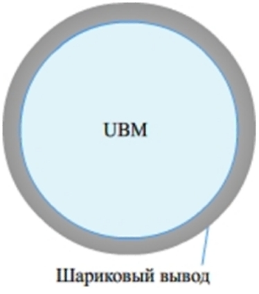
Fig. 8 Location of the UBM layer and the ball (top view).
UBM is located directly below the ball terminal (if you look at the crystal from the side of the balls). When placed on top of each other, the ball exerts voltage on the UBM and can disconnect with the metal layer of the UBM or from the UBM itself.
Some disconnections of the ball will not affect the operation of the device, for example, if there are a large number of power balls connected in parallel, disconnecting one of them will not lead to a malfunction of the device. But if the disconnection occurs on the line along which the data goes ... Such a problem called the “chip blade” and leads to malfunctions in the device. So, it falls off / the ball fell off not between the substrate and the board (although this can be), but between the crystal and the substrate. With a high degree of probability, the destruction of the contact of the ball occurred at the soldering point to the UBM due to the numerous heating / cooling cycles of the crystal. And video cards warm up quickly and to high temperatures, which leads to mechanical stress. Therefore, the rule of law is true, the better the cooling and the “colder” the system, the longer it will last.
According to the Internet, you can stick a video card with a fallen off crystal! (and not with another problem, and then screaming that everything was repaired and the author is wrong) in the oven and warm up, and the video card will work again. You do not need to do this, because you can poison the plastic / textolite in pairs and this will not repair the video card. For some time, operability can be restored, because due to thermal expansion, an oxide layer can break through, but for a long time, until the corrosion / thermal expansion process again disconnects the contact, and this will happen. The only reason it makes sense to warm the video card is for diagnostics, to accurately determine the blade.
One of such hidden technologies for which we pay when buying a processor, phone, video card and other devices - UBM (under bump metallization) is the metallization of a platform on a chip for mounting ball leads.
The development of microelectronics leads to an increase in the density of integration of the components both on the IC chip and on the PCB. If there are not too many conclusions on the crystal, from one to a couple of hundreds or more, then the crystal can be designed for wire welding. There are many examples: flash memory, RAM chips, sound chips, and more. Here, the reader can recall how some of the microcircuit cases look, and say that the cases are soldered to the ball terminals, and he will be right. Only inside these cases are crystals glued and welded with wire. Next, we will talk about ball leads located between the crystal and the body.
Fig. 1 Hunix RAM Chip. Crystal unpacking (white lines) and
the crystal itself (dark rectangle) are shown schematically , although the case itself is soldered on balls.
If the number of pins of a potential crystal is large, from 600 to over 4000, then the developer develops a crystal immediately for ball pins, for example, such crystals as CPU and GPU. Yes, and physically unzipping a wire with such a number of conclusions is a long sequential process, but I generally keep quiet about programming a machine.
Fig. 2 AMD Fiji graphics chip. On the IC chip, more than 4000 solder balls, not on the body.
The ball lead is a ball of solder (it can be lead-containing or without it), which performs 3 functions at the same time:
1. Holds the crystal on a textolite or silicon interposer (like AMD Fiji)
2. Serves to remove heat
3. Creates an electrical connection of the crystal with the external environment
If the crystal is made for ball leads, then copper contact pads are formed over the entire surface of the crystal in the form of a matrix, and are essentially a continuation of the crystal topology. Then, on a copper, where necessary, a passivation protective layer is applied, and is not applied where the ball will be located. The open area of copper is covered with a UBM layer and after that it is ready to apply the ball. Part of the UBM layer rests on passivation, thereby completely covering the copper and creating a protrusion around the perimeter of the site.
Fig. 3 KP under a ball conclusion. Yellow - copper under passivation, gray - UBM coating.
If the crystal is made for wire welding, then the contact pads (KP) for welding are rectangles with a coating mainly of aluminum, and are located around the perimeter of the crystal.
It is also impossible to directly connect a solder ball to such a KP: solder cannot be soldered to an aluminum pad. To do this, solder the ball, also use UBM technology.
And so, UBM is the layer between the solder ball and the metal of the contact pad on the chip. Its task is adhesion with a contact pad, diffusion protection and wettability for solder. UBM is needed to create structures with ball joints and it also allows you to create structures for balls and on ICs created for splicing.
Fig. 5 Location of the UBM
The UBM interface must ensure that the following conditions are met:
1. Create a reliable connection with the aluminum of the contact pad and with the passivation layer on the chip. It is important that the passivation layer itself be without small holes, because this can lead to a short circuit when creating conductive UBM layers.
2. Have a low resistance with a contact pad. To fulfill this requirement, alumina is removed from the surface of the CP before applying the first UBM layer.
3. Provide a barrier to the diffusion of the solder ball material and the KP material.
4. The outer layer of UBM must be wettable for solder.
5. Protect against the formation of an oxide layer on an open surface.
6. Provide as little voltage to the crystal as possible.
UBM is a minimum of 3 etched layers of thin metal films.
1. A layer of adhesion to the KP. It serves to form a bond between the metal of the KP and the passivation layer of the IC and protects against diffusion between the KP and the solder ball. Commonly used materials for this are: Chrome (Cr), titanium (Ti), titanium / tungsten (Ti / W), nickel (Ni), Mo molybdenum. The thickness of this layer is about 0.15 - 0.2 μm.
2. A layer wetted for solder. To create a solder joint with a solder ball. The metals used are: Copper (Cu), Nickel (Ni), Palladium (Pd). The usual layer thickness is ~ 1 - 5 μm.
3. Layer of protection against oxidation. For this, gold (Au) is used. Thickness ~ 0.05 - 0.1 μm.
You can make many combinations of UBM layers, for example, Ti / Cu / Au, Ti / Cu, Ti / Cu / Ni, TiW / Cu / Au, Cr / Cu / Au, Ni / Au, Ti / Ni / Pd, Mo / Pd . However, different UBM structures have different properties and different reliability. For example, Ti / Cu / Ni has better adhesion than Ti / Cu. Combinations of materials UBM affect the reliability of the connection to the site of the crystal, and to the ball of solder. UBM must be compatible with solder ball material. The outer layer of UBM, which works well with lead solders, may not be suitable for lead-free solders. For example, Cu gives a good solder compound with lead solders, and bad with lead-free ones, because pure tin forms an intermetallic compound with copper Sn-Cu. If the copper is completely absorbed by the solder, then the contact will break.
Let's see how it looks on the example of a microcircuit, which was originally developed for wire welding, and then finalized for ball outputs. Moreover, the topology of the crystal did not change for the balls. Indeed, if the crystal works, why climb? This is the WL1271L chip - Texas Instruments Wi-Fi and Bluetooth chip. In the photo, a fragment of it:
Fig. 6 Fragment of a crystal WL1271L.
Here, the moment attracts the attention that there is the possibility, without resorting to changing the topology of the crystal, to adapt it to the ball leads by forming layers on top of the crystal. This requires additional operations on the plate with crystals, the operation of forming balls, but this gives an advantage in saving space on the board, because with a ball size of 200 - 250 μm, it does not need an adapter board, that is, you can mount the crystal directly on the board. As far as I know, they do not do this in Russia, although there are microcircuits that are suitable for this, but some imported ICs do this. In a good way, such a technology should reduce the cost of the final product. For the military, it may not be suitable because of the requirements of reliability, but for home use, at an affordable price, it’s quite.
Now let's look at an example of an IC, which is designed specifically for ball terminals. We take a video card, and we crack the crystal, we clean it, we pickle it with a mixture of ammonium persulfate and copper sulfate.
Fig. 7 Contact pad before (left) and after etching (right).
When tin is etched (and the balls must be leadless), tin displaces copper from copper sulfate, and then this copper in the form of metal is absorbed by ammonium persulfate. Thus, the site is cleared of tin. Under the microscope, when the focus changes, a depression is visible after the tin is removed, this is not so clearly visible in the photo. Copper wires diverging from the contact pad were not etched because they are protected by passivation. The copper under the contact pad itself also remained untouched, because the upper layer of UBM did not react with either ammonium persulfate or sulfate, thereby exposing itself and by this property it is possible to guess what kind of metal it is.
Now about the problem of ball conclusions. During wire splicing, the crystal connects to the casing with aluminum / gold wire, and even if it is deformed, the connection will remain, because the wire is plastic. But the ball lead is hard, slightly plastic, does not stretch and under certain conditions it can lag behind the contact pad (because in this place the metal thickness is minimal => the load is greater). Destruction / delamination leads to an increase in resistance and an open circuit.
Fig. 8 Location of the UBM layer and the ball (top view).
UBM is located directly below the ball terminal (if you look at the crystal from the side of the balls). When placed on top of each other, the ball exerts voltage on the UBM and can disconnect with the metal layer of the UBM or from the UBM itself.
Some disconnections of the ball will not affect the operation of the device, for example, if there are a large number of power balls connected in parallel, disconnecting one of them will not lead to a malfunction of the device. But if the disconnection occurs on the line along which the data goes ... Such a problem called the “chip blade” and leads to malfunctions in the device. So, it falls off / the ball fell off not between the substrate and the board (although this can be), but between the crystal and the substrate. With a high degree of probability, the destruction of the contact of the ball occurred at the soldering point to the UBM due to the numerous heating / cooling cycles of the crystal. And video cards warm up quickly and to high temperatures, which leads to mechanical stress. Therefore, the rule of law is true, the better the cooling and the “colder” the system, the longer it will last.
According to the Internet, you can stick a video card with a fallen off crystal! (and not with another problem, and then screaming that everything was repaired and the author is wrong) in the oven and warm up, and the video card will work again. You do not need to do this, because you can poison the plastic / textolite in pairs and this will not repair the video card. For some time, operability can be restored, because due to thermal expansion, an oxide layer can break through, but for a long time, until the corrosion / thermal expansion process again disconnects the contact, and this will happen. The only reason it makes sense to warm the video card is for diagnostics, to accurately determine the blade.