Development of a power bank for a laptop. From the layout to the finished product. Part one
I wanted to make an external laptop battery for myself for a long time, 3-4 years ago for working in the park. Although I didn’t realize the dream to draw diagrams and trace boards in Gorky Park or the Bitsevsky Forest (for now), I did make an external battery (let's call it modern - PowerBank). About how this device went from a breadboard model to a final product and why I did what is already on the market under a cat.
Initially, I wanted to write a short article about PowerBank development, but when I started, I realized that one part was indispensable. Therefore, I broke it into 4 parts and now I bring to your attention the first of them: layout (circuitry).
Obviously, the development of any electronic device begins with a technical specification (TOR), so I outlined for myself a number of parameters that my PowerBank should provide:
In addition to the basic requirements, I added a few more:
To start development, I made a block diagram of the future device:

Commenting on the scheme, I could say that I could take the managing director from USB, but I was afraid of the difficulties of developing software for USB (later I realized that it was in vain), so I installed a USART-USB converter.
Since the device was originally developed for itself, it was decided to make the layout mainly from the parts that were in my possession and with which I had already worked (to avoid pitfalls). However, price optimization at this stage was not carried out. Therefore, I chose the following components for PowerBank:
Separately, we touch on the choice of a charger (charger) and a control and management system for Li-ion batteries (Li-ion Battery Management System or BMS). A few years ago, I was repairing laptops and often saw BMS from Texas Instruments in batteries. Therefore, first of all, I began to look for a solution for my device from this manufacturer. It is worth noting that, in general, there is no alternative, since only a few offices produce such chips (TI, Maxim, a bit of LT, ST abandoned, Intersil is exotic for us, maybe there is more, but I don’t know). So wandering around the expanses of ti.com I came across a very interesting chip BQ40Z60RHBRthese are memory and BMS in one chip. I really liked it because it replaced 2 microcircuits. This solution is clearly cheaper than if you do separately the memory and BMS and takes up less space. Main performance characteristics of the BQ40Z60 chip:
The chip is quite new (release of the end of 2014), so there is little information on it and I was a little worried because of this, knowing that BI from TI are quite difficult to program, and this is also a combo (memory + BMS). I also worried a bit about possible jambs in the crystal, but knowing that I would use only the basic functionality, I hoped that there would be no problems. However, looking ahead, I’ll say that it happened.
By the way, it was not in vain that I did not say practically anything about the cells and the configuration of the battery, only now the time has come to move on to the choice. There are several criteria for optimal battery configuration selection:
Given that the output voltage of the 19V device, again, the 4s1p configuration is most advantageous.
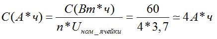
Now we’ll calculate some parameters of the battery under the condition of 60W * h capacity, 4s1p configuration (voltage 14.8V):
The figure I found was too small (well, or the appetite came with a meal) and I decided to switch to 4s2p configuration on LP 5558115 3500mAh cells, which were in stock. Total we have:
Battery capacity: 7A * h (103W * h)
Voltage: 14.8V
This result suited me quite well - it was more than two internal batteries of my laptop (ASUS S451L, 46W * h). The development of the layout began ...
At the layout stage, I wanted to lay some additional features:
I sketched the BQ40Z60 binding circuit from the BQ40Z60EVM-578 debug board, the LTC3780IG binding from its documentation, I did the rest myself. The result is the following scheme .
The scheme is divided into 3 blocks:
Comments on the scheme: the converter unit and the charger + BMS are made according to the schemes from the documentation [1] , [2] , the control unit was made in order to implement a sleep mode for the minimum current consumption in off mode. Looking ahead, I’ll say that in a couple of moments I did it, but with the help of a knife and a soldering iron I was able to make the layout work as it should. The resulting board is shown below: The

board contains 4 layers of 18 μm, the total thickness of 1 mm, ordered on seeedstudio.com.
Now it's time to touch on the main indicator of the quality of iron - this is the efficiency of the entire system as a whole. More precisely, we have 2 efficiency: when charging the battery and when discharging. Strictly speaking, the efficiency of the charge should be optimized only to reduce the heating of the device (assuming that we have a lot of energy for the charge), while the loss of efficiency during the discharge actually reduces the actual capacity of the PowerBank. Let's make a list of the elements that directly affect the efficiency when charging:

ACFET - a transistor that prevents the appearance of voltage on the external power connector when using PowerBank from the battery.
HighSideFET - the upper transistor of the step-down converter of the charger.
LowSideFET - lower transistor of the memory buck converter.
BuckInductor - the throttle of the memory buck converter.
CHGRCS - resistor of the memory current sensor.
CHGFET - battery charging transistor.
DSGFET - discharge transistor battery.
CellCS is a battery current sensor resistor.
Transistors ACFET, CHGFET and DSGFET during operation have only static losses since they are constantly open and are resistors with a resistance equal to the open channel resistance of the Rds_on transistor, so these transistors should have the lowest Rds_on. I chose pqfn3.3x3.3 transistor cases as suitable in power and having a smaller size compared to my favorite pqfn5x6. With the smallest channel resistance of the easily accessible ones were IRFHM830D (Rds_on = 5mOhm + Schottky diode).
The HighSideFET and LowSideFET transistors operate in a pulsed mode, their selection is complicated and will be considered later.
Let’s try to evaluate the losses at the input voltage 19V, battery charge current 4A, configuration 4s1p:
CellCS - the current through it is equal to the charge current, resistance 5mOhm, losses:

CHGRCS - the current through it is equal to the charge current, resistance 10mOhm, losses:

CHGFET and DSGFET - current through of them is equal to the charge current, resistance 5mOhm, total losses:

ACFET - the current through it is equal to the input current (take the maximum possible input current 3.5A is the maximum that a regular laptop memory can give out), resistance 5mOhm, losses:

Here you can add losses on the resistance of the wires of the cell-board, and t Also tracks of the board itself. I calculated them by measuring the voltage drop at a current in the battery circuit of 4A, it was 36mV, which corresponds to power:

BuckInductor - losses in the throttle can be divided into 2 components:
Total total charge losses on static components are:

In order to obtain total charge losses, it is necessary to estimate the losses on the HighSideFET and LowSideFET transistors. The apnot AN-6005 from fairchildsemi helped me with this . In short, on the ControllerDriver tab, add our controller to the database and enter the required parameters in the table:

We take the data from the documentation for BQ40Z60 . Next, fill out the table with the parameters of the HighSideFET and LowSideFET transistors on the MOSFETDatabase tab:

We also take data from the documentation for transistors. I experimented with many transistors (seen from the base) because the conversion frequency in 1 MHz is quite high. Of all the transistors that I could quickly get the best, the CSD17308 from TI turned out to be the best. However, these are just the recommended transistors from the BQ40Z60EVM whale . The best calculations were eGaN transistors from EPC (Efficient Power Conversion), but the price of 500r, a month of waiting and a specific case played against it. A couple more comments from the MOSFETDatabase tab: The
right column - Fig.Merit (Figure of merit - Quality Score) is the product of Rds_on and the Qgsw shutter charge. In general, the lower the Fig.Merit, the better the transistor, but you need to understand that this is a fairly empirical indicator.
On the EfficiencySummary tab, select the controller, the used transistors and their number, set the source parameters and click the Run button.

For a charge current of 4A and an input voltage of 19V, the losses will be 1.17W. Total losses:

After assembling the layout, I measured the charge circuit with the same parameters as in the estimated calculations: the

efficiency of the circuit is 97.1%, while the power loss was 1.908W at the calculated 2.07W. Well, it turned out very close to estimate the loss. The thermogram of the working device is shown in the figure.
Ambient temperature 23 degrees, board without housing. 58 degrees at the hottest point (overheating is 58-23 = 35 degrees) with a foil of 18 μm this is a very good indicator. The throttle at the same time warmed up to 40 - most likely it is heated by transistors. The controller itself warmed up to 52 degrees.
Now we turn to estimating the efficiency of the system during discharge. From the beginning we will evaluate the losses in the converter itself. To do this, we compile a list of elements directly affecting the efficiency:

A is the upper transistor of the lower arm of the LTC3780 converter.
B - lower transistor lowering arm.
C is the lower transistor of the increasing shoulder.
D is the upper transistor of the increasing shoulder.
L - throttle.
RS is the resistor of the current sensor.
And of course the consumption of the LTC3780 controller itself. I will not dwell on the operation of the microcircuit in detail, I can only say that it actually represents a step-down converter standing after a step-up converter with a common inductor. Depending on the input and output voltages, either one part, or the second, or both works (with approximate equality of the input and output voltages).
To calculate the efficiency of the converter, we will use the following parameters:

Let's agree that a laptop always consumes to the maximum. In reality, this is close to the truth, because when connecting an external source, in addition to energy, it also consumes energy to charge the internal battery, and in general, if there is external power, it does not refuse consumption. Voltages correspond to the rated voltage of the cells - 3.7V and low - 3.3V. It is important to note that the converter in the current device always works in boost mode (the input voltage never exceeds the output voltage), but this does not mean that transistors A and B do not switch. To charge the bootstrap capacitor, briefly turn off transistor A and turn on B (the same thing will happen when operating in a lower mode for transistors C and D). For LTC3780, this happens at a frequency of 40kHz.
To estimate the losses, we use the xls file for LTC3780 from the LTpowerCAD2 package. The principle of operation is similar to the previous work with xls for the BQ40Z60. We enter all the values of the output voltage and current, input voltage, the desired conversion frequency, the parameters of the key transistors (I decided to use CSD17308 as in the memory). The inductor was chosen IHLP5050EZER3R3M01 which has a typical DCR = 7.7mOhm. For 3.5A, the inductance is small, it happened because when I purchased components, I was counting on an output current of 4.5A. For the current configuration, the IHLP5050EZER4R7M01 with a typical DCR = 12.8mOhm would be an ideal option. Current sensor - resistor of size 2512 with a resistance of 5mOhm.
After entering all the data in the MOSFETs Power Loss Break Down and Estimated Efficiency fields, there will be pie charts of the component loss distribution and efficiency estimation for the specified input / output voltage and load current.

The efficiency estimate is very optimistic - 98.79% at an input voltage of 14.8V and 98.51% at 13.2V (figures excluding losses in the core of the inductor). The main elements on which losses occur are the inductor / current sensor (23%), transistor A (25%) and D (38% of the total losses).
It's time to measure real efficiency.

The measured efficiency is 96.93% at an input voltage of 14.8V and 96.35% at 13.2V. Let us analyze the data obtained. To do this, we translate the percent efficiency in the power loss:

In this case, the discrepancy is more significant compared with the estimate of losses in the memory converter and amounts to 1.48W. But if we take into account the losses in the core of the inductor (which cannot be neglected with an not optimally selected inductance), the picture will not be so depressing.
Let's estimate the average (at 13.2V) PowerBank efficiency at discharge. It consists of the efficiency of the converter itself, as well as:
CellCS - the current through it is equal to the input current of the converter, resistance is 5mOhm, losses:

CHGFET and DSGFET - the current through them is equal to the input current of the converter, resistance is 5mOhm, total losses:

Then PowerBank efficiency during discharge:

Thermogram the converter with an input voltage of 14.4 V and an output current of 3.5 A is shown below:
The transistor C turned out to be the hottest point, but its heating (at an ambient of 21 degrees) was only 41.1 degrees after 30 minutes of operation. It is clear that in the case these numbers will be higher, but the overheating reserve is huge.
And in conclusion of the first part of the article, I want to say that the work has been done very much, and in the second part of the article we will have a look at hardware and software rakes when starting the layout, configuring the BQ40Z60 and software for STM32F0. I hope it was interesting.
PS: Archive with the draft board and source code will be posted in the following parts of the article.
PPS noticed that it forgot almost the most important thing for this part of the article - a photo of the layout. Correct

On the board you can see traces of corrections, as well as traces of wearing open in a backpack (burnt tracks in the area where the battery is connected). The layout is certainly not the most elegant, but even in this form it can be used.
Initially, I wanted to write a short article about PowerBank development, but when I started, I realized that one part was indispensable. Therefore, I broke it into 4 parts and now I bring to your attention the first of them: layout (circuitry).
Obviously, the development of any electronic device begins with a technical specification (TOR), so I outlined for myself a number of parameters that my PowerBank should provide:
- 19V input voltage (for the possibility of charging from a standard laptop memory)
- 19V output voltage (as with a standard memory)
- maximum output current 3.5A (as with a standard memory)
- cell capacity at least 60W * h (+1 internal battery)
In addition to the basic requirements, I added a few more:
- The efficiency of the converter and the memory is not lower than 94% - to do without radiators.
- The frequency of the converter is not lower than 300 kHz - to reduce the size of the converter itself.
- USB port for viewing basic information about PowerBank such as charge level, health, number of cycles passed, temperature, current and voltage of battery cells, etc.
- Software on PC (Windows) to view basic information about PowerBank.
- The ability to change the output voltage, or the presence of an additional 5V output for charging USB devices.
- LED indication of charge level and PowerBank status.
- Button (Buttons) to turn on the PowerBank and view the charge level.
To start development, I made a block diagram of the future device:
Commenting on the scheme, I could say that I could take the managing director from USB, but I was afraid of the difficulties of developing software for USB (later I realized that it was in vain), so I installed a USART-USB converter.
Since the device was originally developed for itself, it was decided to make the layout mainly from the parts that were in my possession and with which I had already worked (to avoid pitfalls). However, price optimization at this stage was not carried out. Therefore, I chose the following components for PowerBank:
- MK - STM32F051K4U6 with a sight replaced by STM32F042K4U6.
- USART <-> USB to CP2102 Converter. It is not expensive, it works fine, it takes up little space, a run-in solution.
- Switching voltage converter - LTC3780IG . Far from the cheapest / best option, but up-down, maybe 400kHz, has foreign keys, a run-in solution. In the future, a replacement for T51's LM5175 or the use of a synchronous boost converter.
- Linear Stabilizer - LP2951ACD-3.3. He was available, not the best option. Replace own current up to 120 μA with a sight replaced by MCP1703T-3302E / CB with own consumption current up to 5 μA.
- Green and red LEDs size 0805.
- Buttons are ordinary clock SMD.
Separately, we touch on the choice of a charger (charger) and a control and management system for Li-ion batteries (Li-ion Battery Management System or BMS). A few years ago, I was repairing laptops and often saw BMS from Texas Instruments in batteries. Therefore, first of all, I began to look for a solution for my device from this manufacturer. It is worth noting that, in general, there is no alternative, since only a few offices produce such chips (TI, Maxim, a bit of LT, ST abandoned, Intersil is exotic for us, maybe there is more, but I don’t know). So wandering around the expanses of ti.com I came across a very interesting chip BQ40Z60RHBRthese are memory and BMS in one chip. I really liked it because it replaced 2 microcircuits. This solution is clearly cheaper than if you do separately the memory and BMS and takes up less space. Main performance characteristics of the BQ40Z60 chip:
- Charge Current: Up to 4A
- Number of cells: up to 4x
- Conversion Frequency: 1MHz
- Input voltage: up to 25V
- Cell capacity: up to 65A * h
- Balancing function
- Configurable LEDs for indication (charge, capacity)
The chip is quite new (release of the end of 2014), so there is little information on it and I was a little worried because of this, knowing that BI from TI are quite difficult to program, and this is also a combo (memory + BMS). I also worried a bit about possible jambs in the crystal, but knowing that I would use only the basic functionality, I hoped that there would be no problems. However, looking ahead, I’ll say that it happened.
By the way, it was not in vain that I did not say practically anything about the cells and the configuration of the battery, only now the time has come to move on to the choice. There are several criteria for optimal battery configuration selection:
- To reduce losses on the wires, it is necessary to minimize currents between the nodes of the device. With this in mind, a battery of 4 cells connected in series (generally accepted designation 4s1p or 4-serial 1-parallel) is more profitable than 4 parallel cells (1s4p) see figure.

- Since the charge current is limited, in order to increase the power (and speed) of the battery charge, we must increase the voltage. This criterion is also for the 4s1p configuration.
- The efficiency of the converter decreases when the difference between the input and output voltage increases. Here is the chart from the documentation for the MP2307DN converter.

Given that the output voltage of the 19V device, again, the 4s1p configuration is most advantageous.
Now we’ll calculate some parameters of the battery under the condition of 60W * h capacity, 4s1p configuration (voltage 14.8V):
The figure I found was too small (well, or the appetite came with a meal) and I decided to switch to 4s2p configuration on LP 5558115 3500mAh cells, which were in stock. Total we have:
Battery capacity: 7A * h (103W * h)
Voltage: 14.8V
This result suited me quite well - it was more than two internal batteries of my laptop (ASUS S451L, 46W * h). The development of the layout began ...
At the layout stage, I wanted to lay some additional features:
- connected the BQ40Z60 LEDs. They have a functional indication of the charge level with adjustable thresholds, as well as the charging process.
- Added the ability to adjust the frequency / mode of operation (discontinuous or inextricable currents) of the converter (using a PWM MK + RC filter).
I sketched the BQ40Z60 binding circuit from the BQ40Z60EVM-578 debug board, the LTC3780IG binding from its documentation, I did the rest myself. The result is the following scheme .
The scheme is divided into 3 blocks:
- Voltage converter block
- Storage Unit + BMS
- MK control unit
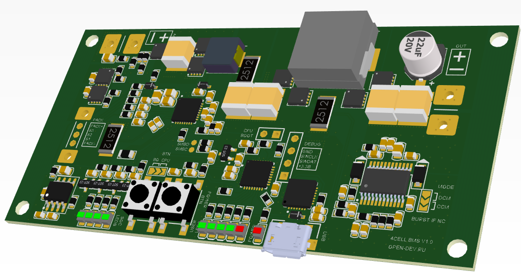
Comments on the scheme: the converter unit and the charger + BMS are made according to the schemes from the documentation [1] , [2] , the control unit was made in order to implement a sleep mode for the minimum current consumption in off mode. Looking ahead, I’ll say that in a couple of moments I did it, but with the help of a knife and a soldering iron I was able to make the layout work as it should. The resulting board is shown below: The
board contains 4 layers of 18 μm, the total thickness of 1 mm, ordered on seeedstudio.com.
Now it's time to touch on the main indicator of the quality of iron - this is the efficiency of the entire system as a whole. More precisely, we have 2 efficiency: when charging the battery and when discharging. Strictly speaking, the efficiency of the charge should be optimized only to reduce the heating of the device (assuming that we have a lot of energy for the charge), while the loss of efficiency during the discharge actually reduces the actual capacity of the PowerBank. Let's make a list of the elements that directly affect the efficiency when charging:
ACFET - a transistor that prevents the appearance of voltage on the external power connector when using PowerBank from the battery.
HighSideFET - the upper transistor of the step-down converter of the charger.
LowSideFET - lower transistor of the memory buck converter.
BuckInductor - the throttle of the memory buck converter.
CHGRCS - resistor of the memory current sensor.
CHGFET - battery charging transistor.
DSGFET - discharge transistor battery.
CellCS is a battery current sensor resistor.
Transistors ACFET, CHGFET and DSGFET during operation have only static losses since they are constantly open and are resistors with a resistance equal to the open channel resistance of the Rds_on transistor, so these transistors should have the lowest Rds_on. I chose pqfn3.3x3.3 transistor cases as suitable in power and having a smaller size compared to my favorite pqfn5x6. With the smallest channel resistance of the easily accessible ones were IRFHM830D (Rds_on = 5mOhm + Schottky diode).
The HighSideFET and LowSideFET transistors operate in a pulsed mode, their selection is complicated and will be considered later.
Let’s try to evaluate the losses at the input voltage 19V, battery charge current 4A, configuration 4s1p:
CellCS - the current through it is equal to the charge current, resistance 5mOhm, losses:
CHGRCS - the current through it is equal to the charge current, resistance 10mOhm, losses:
CHGFET and DSGFET - current through of them is equal to the charge current, resistance 5mOhm, total losses:
ACFET - the current through it is equal to the input current (take the maximum possible input current 3.5A is the maximum that a regular laptop memory can give out), resistance 5mOhm, losses:
Here you can add losses on the resistance of the wires of the cell-board, and t Also tracks of the board itself. I calculated them by measuring the voltage drop at a current in the battery circuit of 4A, it was 36mV, which corresponds to power:
BuckInductor - losses in the throttle can be divided into 2 components:
- losses on the active resistance of the winding (DCR - dc winding resistance). For the selected inductor IHLP2525CZER2R2M01, the typical value is DCR = 18mOhm, which with an average current of 4A will cause losses:

- Losses in the core are quite difficult to calculate, having only data from the documentation, so we believe Vishay’s assurances that their materials are super cool, and we also have current ripples in the region of 20%, so we take the core losses to zero.
Total total charge losses on static components are:
In order to obtain total charge losses, it is necessary to estimate the losses on the HighSideFET and LowSideFET transistors. The apnot AN-6005 from fairchildsemi helped me with this . In short, on the ControllerDriver tab, add our controller to the database and enter the required parameters in the table:
We take the data from the documentation for BQ40Z60 . Next, fill out the table with the parameters of the HighSideFET and LowSideFET transistors on the MOSFETDatabase tab:
We also take data from the documentation for transistors. I experimented with many transistors (seen from the base) because the conversion frequency in 1 MHz is quite high. Of all the transistors that I could quickly get the best, the CSD17308 from TI turned out to be the best. However, these are just the recommended transistors from the BQ40Z60EVM whale . The best calculations were eGaN transistors from EPC (Efficient Power Conversion), but the price of 500r, a month of waiting and a specific case played against it. A couple more comments from the MOSFETDatabase tab: The
right column - Fig.Merit (Figure of merit - Quality Score) is the product of Rds_on and the Qgsw shutter charge. In general, the lower the Fig.Merit, the better the transistor, but you need to understand that this is a fairly empirical indicator.
On the EfficiencySummary tab, select the controller, the used transistors and their number, set the source parameters and click the Run button.
For a charge current of 4A and an input voltage of 19V, the losses will be 1.17W. Total losses:
After assembling the layout, I measured the charge circuit with the same parameters as in the estimated calculations: the
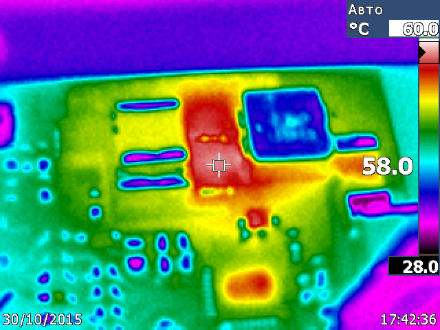
efficiency of the circuit is 97.1%, while the power loss was 1.908W at the calculated 2.07W. Well, it turned out very close to estimate the loss. The thermogram of the working device is shown in the figure.
Ambient temperature 23 degrees, board without housing. 58 degrees at the hottest point (overheating is 58-23 = 35 degrees) with a foil of 18 μm this is a very good indicator. The throttle at the same time warmed up to 40 - most likely it is heated by transistors. The controller itself warmed up to 52 degrees.
Now we turn to estimating the efficiency of the system during discharge. From the beginning we will evaluate the losses in the converter itself. To do this, we compile a list of elements directly affecting the efficiency:
A is the upper transistor of the lower arm of the LTC3780 converter.
B - lower transistor lowering arm.
C is the lower transistor of the increasing shoulder.
D is the upper transistor of the increasing shoulder.
L - throttle.
RS is the resistor of the current sensor.
And of course the consumption of the LTC3780 controller itself. I will not dwell on the operation of the microcircuit in detail, I can only say that it actually represents a step-down converter standing after a step-up converter with a common inductor. Depending on the input and output voltages, either one part, or the second, or both works (with approximate equality of the input and output voltages).
To calculate the efficiency of the converter, we will use the following parameters:
Let's agree that a laptop always consumes to the maximum. In reality, this is close to the truth, because when connecting an external source, in addition to energy, it also consumes energy to charge the internal battery, and in general, if there is external power, it does not refuse consumption. Voltages correspond to the rated voltage of the cells - 3.7V and low - 3.3V. It is important to note that the converter in the current device always works in boost mode (the input voltage never exceeds the output voltage), but this does not mean that transistors A and B do not switch. To charge the bootstrap capacitor, briefly turn off transistor A and turn on B (the same thing will happen when operating in a lower mode for transistors C and D). For LTC3780, this happens at a frequency of 40kHz.
To estimate the losses, we use the xls file for LTC3780 from the LTpowerCAD2 package. The principle of operation is similar to the previous work with xls for the BQ40Z60. We enter all the values of the output voltage and current, input voltage, the desired conversion frequency, the parameters of the key transistors (I decided to use CSD17308 as in the memory). The inductor was chosen IHLP5050EZER3R3M01 which has a typical DCR = 7.7mOhm. For 3.5A, the inductance is small, it happened because when I purchased components, I was counting on an output current of 4.5A. For the current configuration, the IHLP5050EZER4R7M01 with a typical DCR = 12.8mOhm would be an ideal option. Current sensor - resistor of size 2512 with a resistance of 5mOhm.
After entering all the data in the MOSFETs Power Loss Break Down and Estimated Efficiency fields, there will be pie charts of the component loss distribution and efficiency estimation for the specified input / output voltage and load current.
The efficiency estimate is very optimistic - 98.79% at an input voltage of 14.8V and 98.51% at 13.2V (figures excluding losses in the core of the inductor). The main elements on which losses occur are the inductor / current sensor (23%), transistor A (25%) and D (38% of the total losses).
It's time to measure real efficiency.
The measured efficiency is 96.93% at an input voltage of 14.8V and 96.35% at 13.2V. Let us analyze the data obtained. To do this, we translate the percent efficiency in the power loss:
In this case, the discrepancy is more significant compared with the estimate of losses in the memory converter and amounts to 1.48W. But if we take into account the losses in the core of the inductor (which cannot be neglected with an not optimally selected inductance), the picture will not be so depressing.
Let's estimate the average (at 13.2V) PowerBank efficiency at discharge. It consists of the efficiency of the converter itself, as well as:
CellCS - the current through it is equal to the input current of the converter, resistance is 5mOhm, losses:
CHGFET and DSGFET - the current through them is equal to the input current of the converter, resistance is 5mOhm, total losses:
Then PowerBank efficiency during discharge:
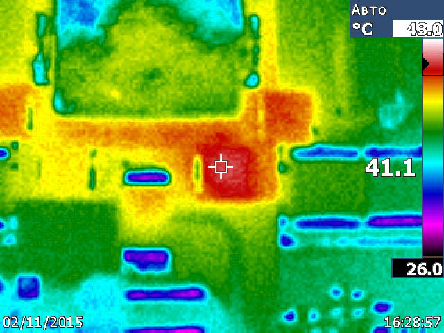
Thermogram the converter with an input voltage of 14.4 V and an output current of 3.5 A is shown below:
The transistor C turned out to be the hottest point, but its heating (at an ambient of 21 degrees) was only 41.1 degrees after 30 minutes of operation. It is clear that in the case these numbers will be higher, but the overheating reserve is huge.
And in conclusion of the first part of the article, I want to say that the work has been done very much, and in the second part of the article we will have a look at hardware and software rakes when starting the layout, configuring the BQ40Z60 and software for STM32F0. I hope it was interesting.
PS: Archive with the draft board and source code will be posted in the following parts of the article.
PPS noticed that it forgot almost the most important thing for this part of the article - a photo of the layout. Correct
On the board you can see traces of corrections, as well as traces of wearing open in a backpack (burnt tracks in the area where the battery is connected). The layout is certainly not the most elegant, but even in this form it can be used.