AMD's First High Bandwidth Memory Cards to appear in a Few Months
A new type of memory is designed to provide further performance gains.
 According to AMD itself, the company has for years defined new types of memory for graphics accelerators, and the rest of the industry has been catching up. This gave AMD products a competitive advantage, for example, at the time, the innovation in the form of GDDR5 provided the Radeon HD 4870 with leadership in performance. As a result, GDDR5 became the standard, but seven years have passed since its first appearance, and no fundamentally new changes have occurred. The next breakthrough is to provide the High Bandwidth Memory standard. The first video accelerator based on it can come out in a few months.
Work on HBM began seven years ago, that is, around the same time that GDDR5 was completely ready. The same engineers worked on the technology, says AMD employee Joe Macri. Even then, they began to worry about the growing dependence of the total computing power of personal computers on memory, and they began to suspect that power consumption would gradually become a deterrent.
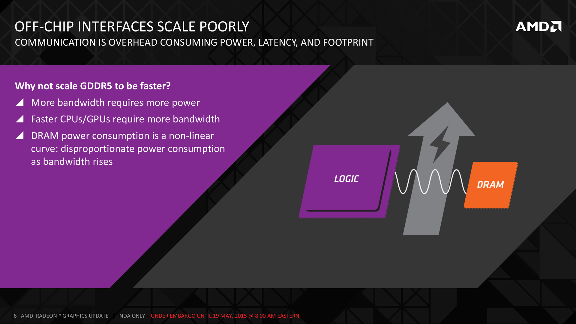
Now everything is squeezed out of GDDR5. To get additional bandwidth, you have to add additional chips and channels that eat away board space and energy. Everything has its limits, and the latest generation video cards demonstrate them with their 512-bit interfaces. The usual GDDR5 acceleration stops working - this year Samsung started producing chips at 8 Gb / s, which is an improvement of only 14% over the previous maximum (7 Gb / s). AMD has already begun to experience problems with further acceleration, as increasing the frequency means a sharp increase in power consumption.

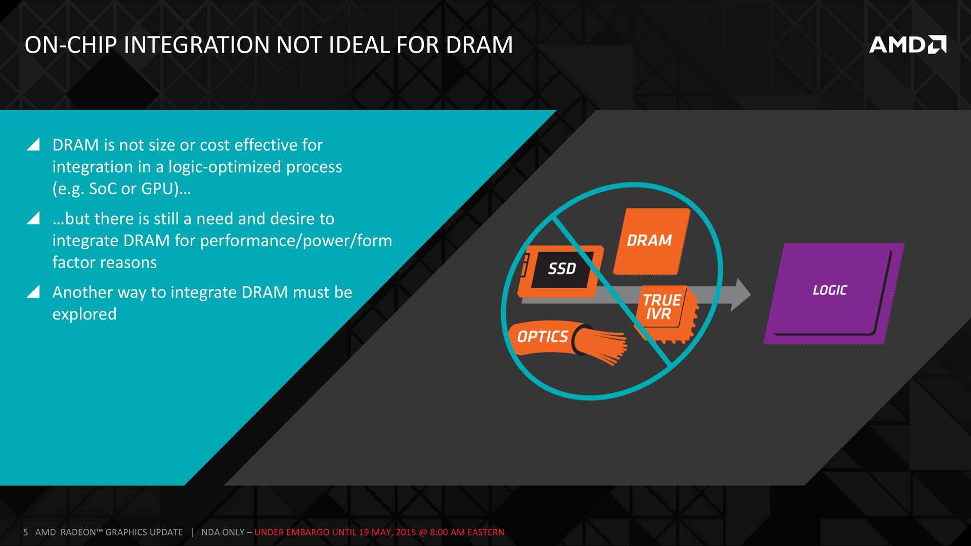
One solution to this problem is what manufacturers have been doing for the last couple of decades to reduce cost and energy and increase productivity: integration. For example, the central processors included a lot of elements, from mathematical coprocessors to memory controllers, and in each case there were pluses. But combining memory and GPUs is not such a simple process, explains Macri. The processes of their production are so different that their combination on one chip has become too expensive. The solution is to place the memory close to the GPU, but on a separate chip. HBM involves placing multiple layers in a 3D configuration (or, more precisely, 2.5D).
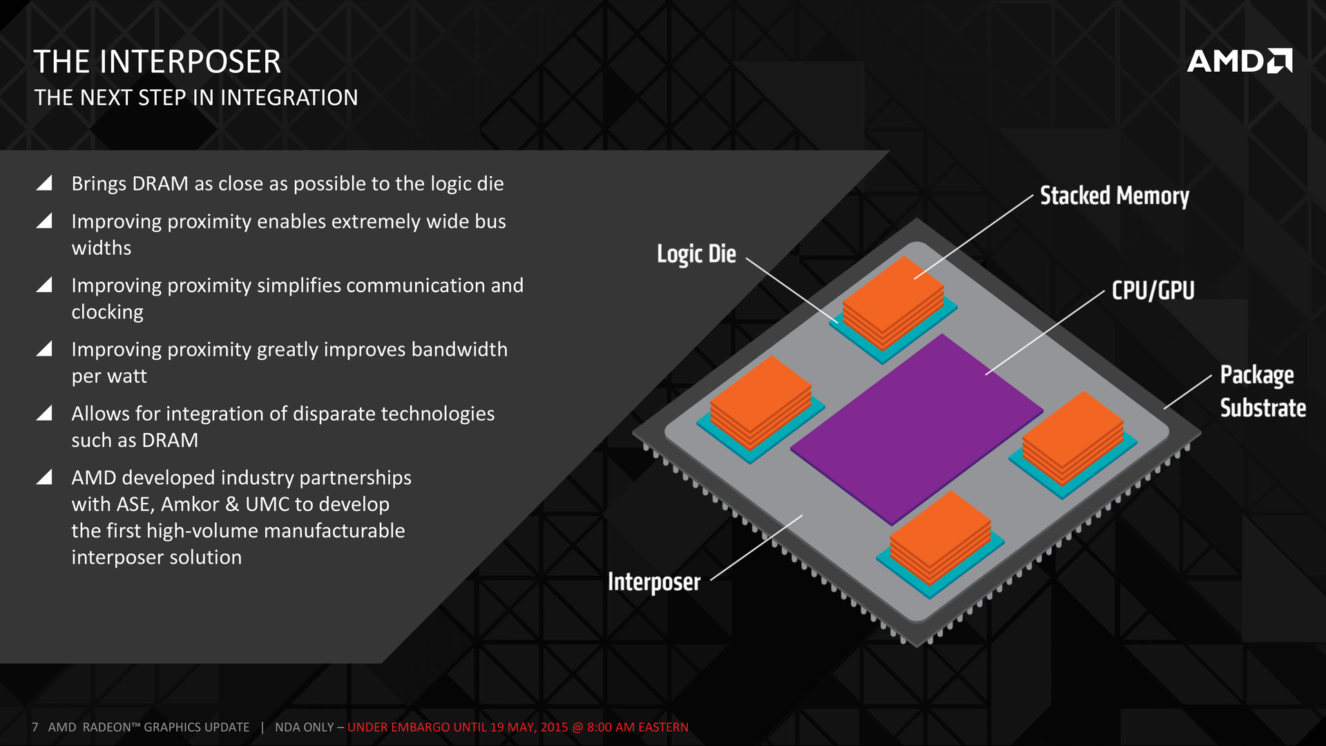
HBM consists of three main parts: this is the main chip (CPU, GPU or system on a chip), one or more memory columns and the silicon layer on which they are located - interposer (intermediary). Interposer is a regular silicon chip, currently manufactured using the older 65 nm process technology. Macri explained that the role of the interposer is completely passive, it has no active elements, since its only task is to electrically connect the tracks between the memory and the processor. Since it is a silicon chip, it can connect much more elements than a regular board. Interposer is the key part of High Bandwidth Memory. Other traditional elements are located under the interposer, but their task is to exchange with the PCI Express bus, output to monitors and other interfaces.
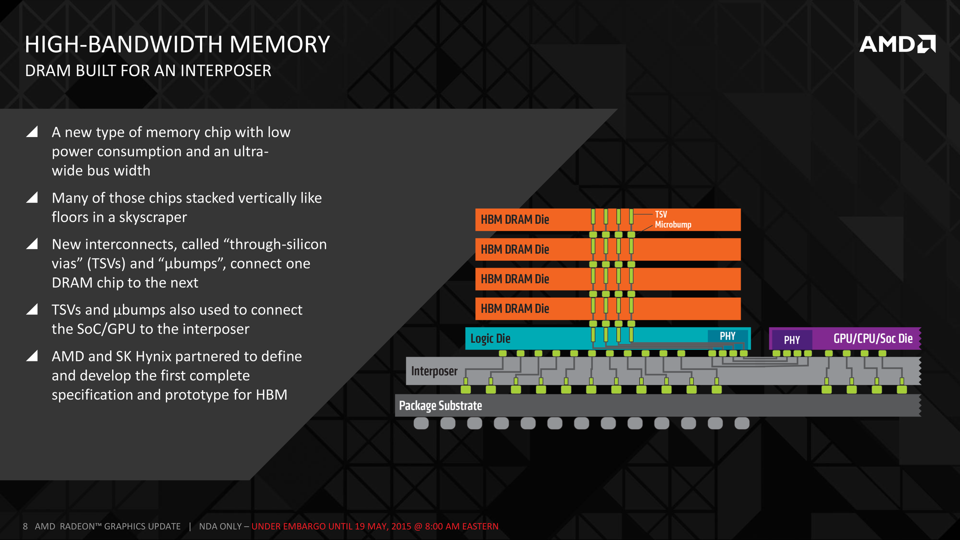
The interposer is of great interest, but another important new feature is the layered memory. Four layers of the actual memory are stacked on the logical layer controlling the operation. Five layers are connected to each other using interconnects in a silicon substrate (TSV). According to Macri, these layers are very thin, the thickness reaches about 100 micrometers. If you take one in your hand, it will bend and wave like paper.
And each of these storage layers contains a new type of memory, specially created for working conditions in HBM. The memory uses a relatively low voltage - 1.3 volts (GDDR5 has 1.5), lower operating frequencies (500 MHz instead of 1750) and has lower bandwidth (1 GB / s instead of 7). All this is offset by a very wide interface. In the first HBM implementation, each memory layer communicates on two 128-bit channels, that is, each stack has a 1024-bit bus. The result is a massive 4096-bit memory with a bandwidth of about 128 GB / s.

High Bandwidth Memory did not appear from scratch. In 2011, AMD announced plans to collaborate with the Hynix memory manufacturer (now SK Hynix) to develop and implement the next-generation memory standard. AMD has created connections, an interposer and a new type of memory. Hynix produces memory, and the first samples of the interposer were created at the facilities of United Microelectronics Corporation. The new standard has already been approved by the JEDEC memory industry regulatory. This means that High Bandwidth Memory can be widely supported by various companies. With some delay, HBM also fell into Nvidia's plans.
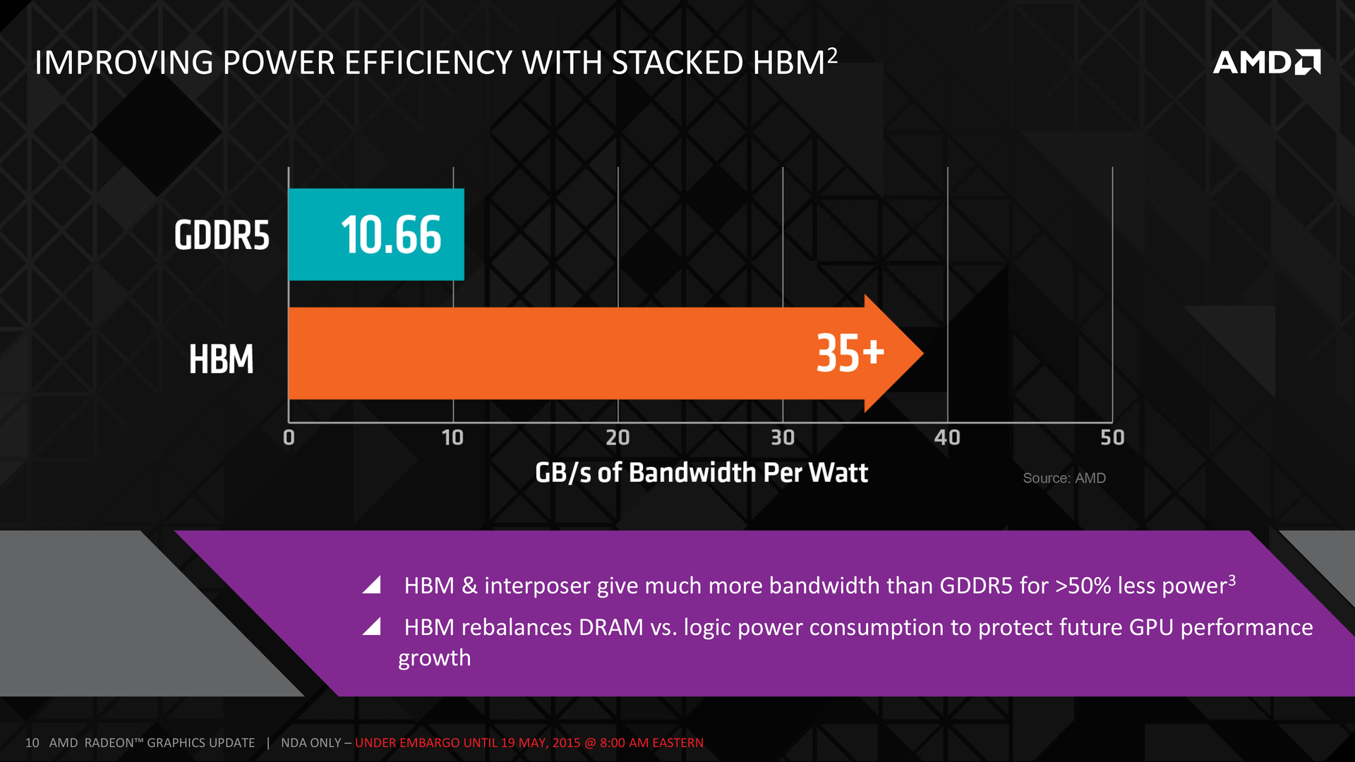
Even the first generation implementation of High Bandwidth Memory has a number of advantages over GDDR5, and this is not only peak bandwidth. According to Macri, GDDR5 allows you to transfer 10.66 GB / s per watt, and with HBM this figure is 35. Energy efficiency of the memory is an important indicator, since the R9 290X spends 15-20% of energy specifically for memory. Switching to HBM will lower this indicator by more than two times.
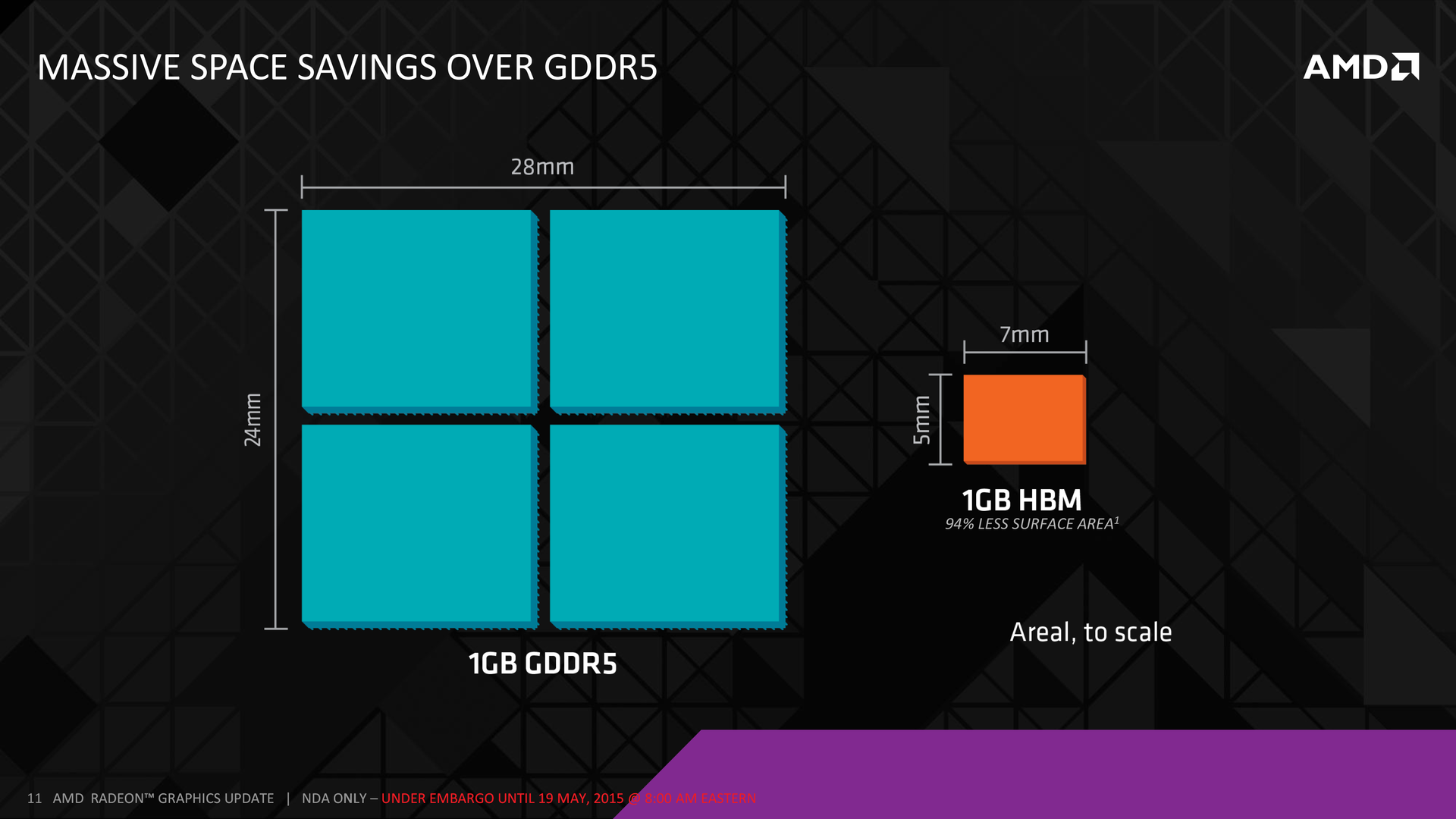
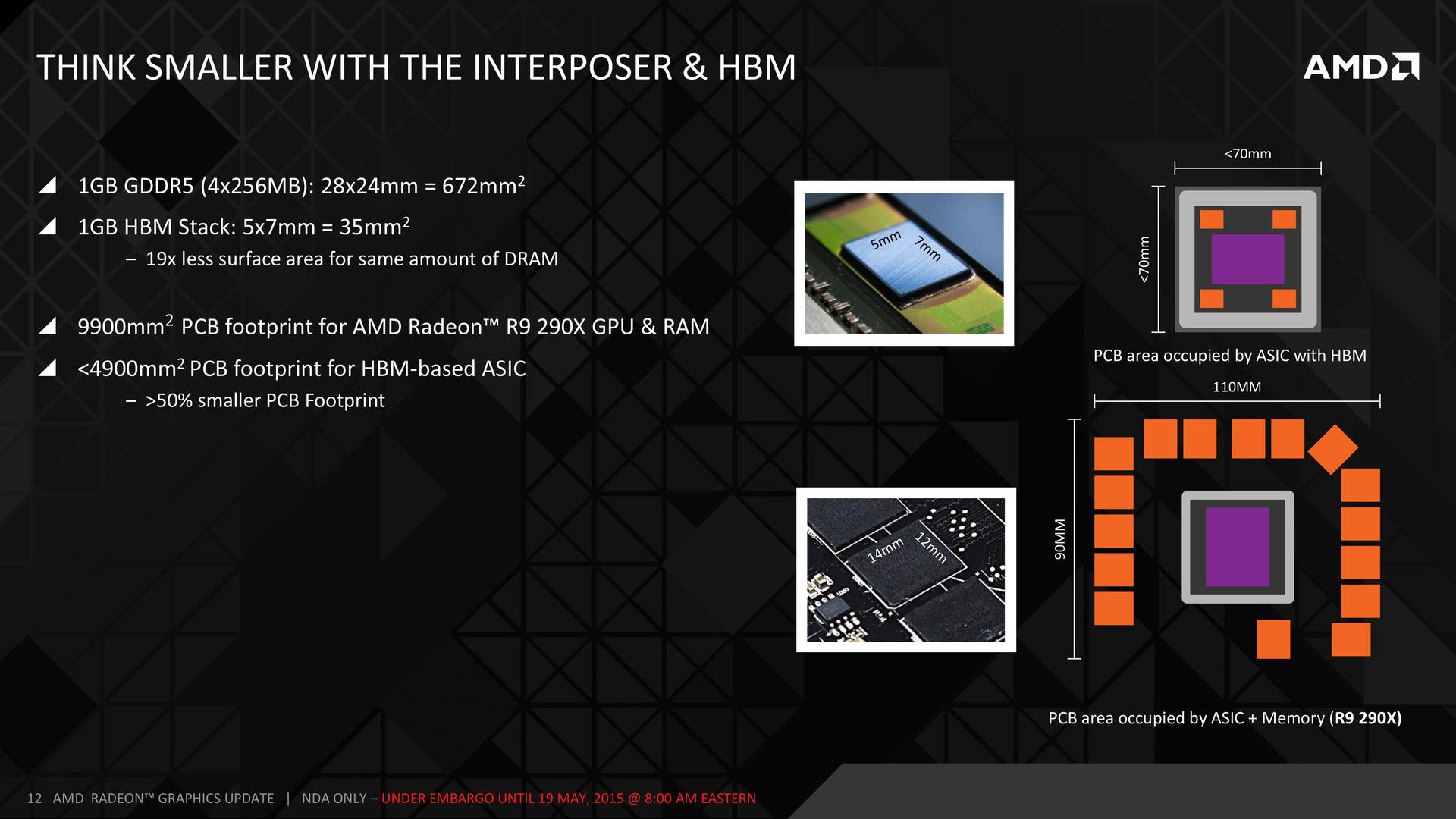
The memory is not only more energy efficient, it is compact. A gigabyte in HBM requires 35 mm², and four GDDR5 chips of the same volume occupy 672 mm² of board area. Therefore, HBM will allow the creation of more compact devices. The interposer is organized very efficiently, which reduces the overall crystal size. It is even possible to improve the data flow inside the video card. In total, approximately two times less board area is required, this will simplify the construction of cards with two video processors. The memory of the post-GDDR era will change not only video accelerators, but also APUs. More channels promise less random access time. A simplified clocking system and other minor changes mean a potential reduction in response time. Macri expects HBM to penetrate many areas of the computer market.
The first generation HBM implementation has an important minus: the total memory size can reach only 4 GB. This is a bit if you recall that the Titan X has three times as much, 12 GB of memory, and the current generation R9 290X has the same 4 GB. Even flagship limits are easy to achieve in 4K resolution. But Macri claims that AMD will somehow cope with this limitation. In his opinion, video cards of the current generation do not handle memory very efficiently. The memory volumes grew rapidly, so AMD had not thought much about using them until now.
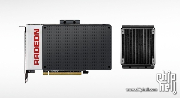
HBM also has other "childhood" problems. For example, the size of video processor microcircuits is growing, and the interposer should be even larger, and the cost of its production can reach prohibitively high values. The small size of HBM will mean the cooling problems that were already in some early instances of the R9 290X. According to Macri, although the illustrations suggest otherwise, the stacks of memory are about the same height as the video processor, so they increase the total area of heat dissipation. Finally, the new technology must pay off, and for this new solutions must be produced and sold in large volumes. According to leaks, the three hundredth series will be presented on June 18, and the R9 390X will be shown on June 24. Leaks in photographs hint at possible liquid cooling.
Macri said a second version of High Bandwidth Memory is already being developed. Its throughput is two times higher than that of the first generation, and the number of memory layers will jump to eight. Through the use of the new process technology, the volume will increase four times. Macri is confident that someday the number of memory layers can grow to 16.
For the first time, HBM will appear in the next generation of AMD graphics cards. Various assumptions about their future characteristics give some possible estimates.
| AMD Radeon R9 290X | Nvidia GeForce GTX Titan X | Future flagship - media speculation | |
|---|---|---|---|
| Memory size | 4 GB | 12 GB | 4 GB |
| Memory chip bandwidth | 5 Gbps | 7 Gbps | 1 Gbps |
| Number of chips | 16 | 24 | 4 |
| Chip throughput | 20 GB / s | 14 GB / s | 128 GB / s |
| Memory bus | 512 bit | 384 bit | 4096 bit |
| Total throughput | 320 GB / s | 336 GB / s | 512 GB / s |
| Estimated Memory Consumption | 30 watts | 31.5 watts | 14.6 watts |
Based on Tech Report , ExtremeTech and AnandTech .
