ECO Flow in Vivado or working in netlist editing mode
- From the sandbox
- Tutorial
annotation
The article describes the Vivado operating mode, which allows you to make changes to the project at the editing level of the list of connections (hereinafter - netlist). The ECO mode itself is described, as well as some nuances that appear while working in it. A demonstration example is given and a complete sequence of actions is described to obtain a result, which anyone can verify the operability of. This article will be useful for the “general development” of FPGA developers, and especially those who often debug projects in Logic Analyzer. I hope that working in this mode will be of interest to developers working with large crystals, the compilation time of which can reach hours (or even tens of hours), since in this mode the time spent on implementation can be reduced to literally when making changes to the netlist a couple of minutes.

Table of contents
- annotation
- Введение
- 1. ECO: краткий обзор
- 2. Design Сheckpoint
- 3. Разработка тестового проекта
- 3.1. Создание проекта
- 3.2. Создание и добавление HDL файлов в проект
- 3.3.Создание проекта MicroBlaze и работа в IP Integrator
- 3.4.Синтез и имплементация
- 3.5.Написание программы для MicroBlaze
- 3.6.Запуск программы и отладка
- 4. Переход в режим ECO
- 5. ECO: описание интерфейса
- 6. Внесение изменений в проект
- 6.1. Создание новых элементов в нетлисте
- 6.2. Изменение свойств/параметров компонентов
- 6.3. Подключение других цепей к пробникам и ILA
- 6.4. Замена портов ввода/вывода
- 7. Сравнительный анализ
- 8. Заключение
- 9. Домашнее задание
- Библиографический список
The article has a lot of pictures not in spoilers (140 pieces). Please be careful if you come in from the phone.
Introduction
Often, when I have to give a lecture or conduct a seminar, I always try to tell a little more than the program suggests. So it was at the last three seminars on working with single-core Zynq-7000S. This time it was interesting to see how much the audience knows about some of the “hidden” modes of working with Vivado. The question was quite simple: “Does anyone present know about the ECO Flow mode?” Immediately after the question was followed by what is called “forest of hands, which I was not particularly surprised at.
The desire to somewhat enlighten the developers at least about the presence of this mode in Vivado, not to mention the demonstration of working in it, appeared to me a very long time ago. But for some mysterious reason, I “harnessed” to write guides for building projects using MicroBlaze and working with it. However, after recent seminars, it became obvious that writing about ECO Flow is still necessary.
The purpose of the article is to give a general idea of the ECO mode in the Vivado environment [1] provided by Xilinx for its crystals and to show how it works in a real example, trying to indicate “subtle” points and analyze its advantages and disadvantages.
The tasks that are set in this article:
- to develop a test example, if possible containing and demonstrating all (or at least most) of the possibilities of working in ECO mode;
- to implement the project;
- Explain the concept of Design Checkpoint;
- Describe the transition to ECO mode of operation;
- make changes to the netlist and get the FPGA firmware file;
- make sure that the changes made are correct;
- compile a summary table of the time spent on standard changes to the project and compare it with the time spent in ECO mode, as well as incremental implementation.
Unfortunately, I do not have the opportunity to physically verify the methodology on a fairly “heavy” chip (for example, Virtex UltraScale). But, I think, even the example that will be given - with a test on the modest Artix-7 installed on the Arty board [2], will be quite indicative. In the process of writing, I will rely on several basic documents that describe the ECO mode [3], [4], [5]. The used version of Vivado (and, accordingly, the documentation) is 2017.4.
A small digression: yes, there are a lot of pictures and “trivialities” in the manual on how to create a project, build a processor system on MicroBlaze, work in IP Integrator, debugging, etc. If you are experienced and just want to read about ECO, please go directly to chapter 4: “Switching to ECO mode”. If you don’t know how to build a project on MicroBlaze, you have never worked in IP Integrator, or like the guides in the style of step-by-step illustrations, I will be only glad if you take an additional 75-90 minutes to the material presented. And yet, I hope that someone will complete the manual completely, with verification in hardware.
1. ECO: an overview
ECO - Engineering change orders [6] - this is a mode in which it is possible to make changes to a netlist, a synthesized or implemented project with minimal impact on the original netlist. Vivado has an ECO mode in which it is possible to change the so-called Design Checkpoint of a project (see below), implement the changes made, generate the necessary reports for the changed netlist and generate an FPGA firmware file from it.
The most typical application of this mode:
- Modification of probes and connected lines of logic analyzers (ILA - IntegratedLogicAnalyzer) during project debugging. The user can change the set of lines connected to ILA, while avoiding the complete re-implementation of the project.
- Reassignment of circuits connected to the FPGA legs. If the project developer, circuit designer, or PCB developer made a mistake in assigning the legs (for example, rx is confused with tx), and the FPGA project has already been implemented, this way you can reassign the ports in netlist, avoiding re-full implementation (t i.e. synthesis, mapping, optimization, placement, tracing - with all associated costs of machine time and resources) of the project.
- Performing a “What_if?” Analysis (editing the contents of memory, changing the functionality of LUT, improving timings, etc.)
The main task of working in ECO mode is to save time and avoid re-implementing the project when making changes at the setup or debugging stage of the project. Many are familiar with the incremental implementation mode, which is also used in ECO, but in ECO, compared to incremental implementation, it is faster to get the firmware file and faster to execute the current debug iteration.
Note: ECO operation is only possible with Design Checkpoint.
2. Design Checkpoint
The design route is divided into several components: including synthesis and implementation. Implementation, in turn, is divided into sub-stages: various optimizations, placement and tracing. The intermediate stages of the design route are stored in a “container” called Design Checkpoint (DCP) [7]. This is a file with the extension “.dcp”. Design Checkpoint contains:
- The current netlist (depending on the stage of the design route), including all optimizations performed before writing the dcp file.
- The constraints imposed on the project (design constraints).
By default, Vivado creates four dcp files: one - at the stage of synthesis of the top-level module of the project (if synthesis is performed in out-of-context mode, then for all modules that are synthesized in out-of-context, its own dcp file is created) and three - at the implementation stage. These files can be found in the folders:
“Project_name.runs / synthesis_name / top_module_name.dcp”
“Project_name.runs / implementation_name /”.
In fig. Figure 1 shows an example of the location and .dcp files that are created by default for some abstract project.
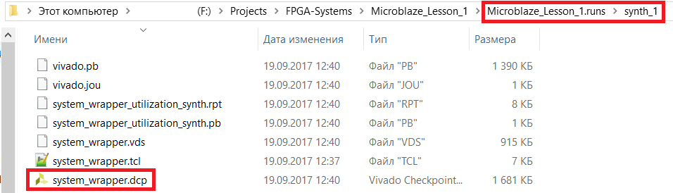
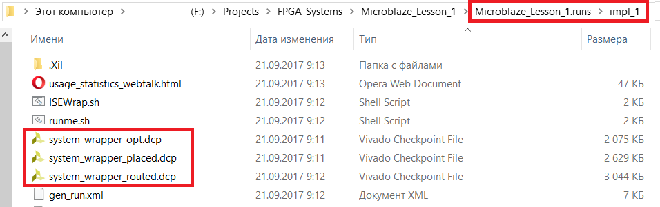
Figure 1 - dcp files created by default (1 - “postsynthesis-” and 3 - “post-implementation-”: after optimization (_opt), after placement (_placed) and after tracing (_routed))
In the project mode of work with Vivado (Project Mode [8]) .dcp files are created automatically. But when working in non-project mode (Non-ProjectMode [8]), the user himself must ensure that "snapshots" of the current state of the project are recorded. To do this, use the appropriate Tcl commands [9, 10] .:
write_checkpoint <file_name>.dcp
read_checkpoint <file_name>.dcp
About why, how and what dcp files should be opened, will be described later.
3. Development of a test project
To demonstrate ECO capabilities on a test project, it should contain the following:
- Elements that are not in the original netlist or elements for which functionality can be changed. For example, turn on the LED on the button - and in the original project it will light up by pressing, and in the changed project - by pressing it will turn off. That is, it will be necessary to add an inverter to the netlist, which is not in the original project.
- Elements for which content can be changed. For example, the truth table in the LUT or the contents of block memory. Moreover, changing the contents of block memory here will be preferable, since we will already perform the LUT change in step 1, when we will create an additional inverter.
- ILA - for the possibility of replacing connected circuits with other circuits. That is, without touching the ILA itself, we will try through a netlist to replace the circuits selected in the original project connected to it with others.
- Confused conclusions. Suppose that when designing a printed circuit board, its developer performed pin-swap of two pins for the convenience of wiring, without coordinating it with the FPGA developer, i.e. made an error confusing rx with tx UART. In ECO mode, we will need to restore the connection.
3.1. Project creation
We find the Vivado icon and click on it twice, the welcome window will open (Fig. 2)
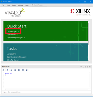
Figure 2 - Vivado Welcome Window
To create a new project, click the Create Project button. Pressing the button brings up the wizard for creating a new project. After its appearance, click the Next button (Fig. 3).
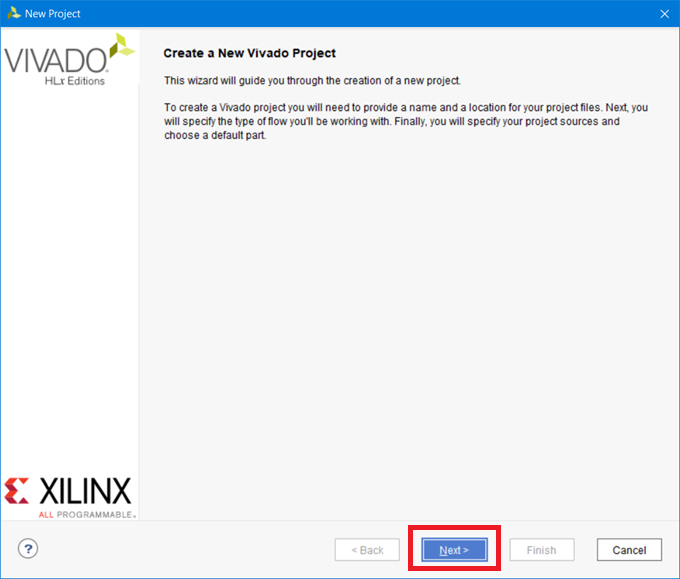
Figure 3 - Window for creating a new project wizard
Enter the name of the project, in the Project Name field write “eco_flow”. We indicate where the project will be located: in the Project location field, specify the directory with the project. I will have it “F: / Projects / FPGA-Systems / eco_flow / projects / vivado”. If you check the “create project subdirectory” checkbox, an additional folder with the project name will be created. Click Next (Fig. 4).

Figure 4 - Entering the name of the project and its location
We create an ordinary project, so just select the RTL project type. At the current stage, we will not add any files to the project, therefore, check “Do not specify sources at this time” and click Next (Fig. 5).
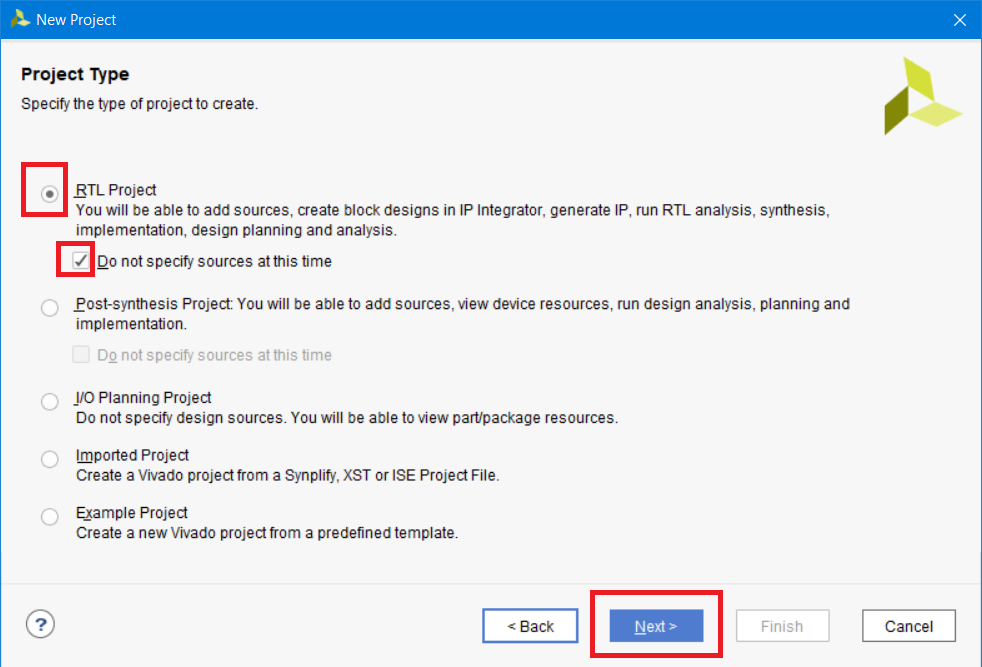
Figure 5 - Selecting the type of project to be created
We will work with the Arty board [2], so we select the crystal that is installed on it: xc7a35tcsg324-1. Click Next (Fig. 6).
Note: I do not specifically select a ready-made board from the template of available boards. This is done so that you can manually make mistakes, which we will then correct.

Figure 6 - Choice of crystal xc7a35tcsg324-1
The final in the new project setup wizard will be the Summary window of the created project. Click Finish (Fig. 7).
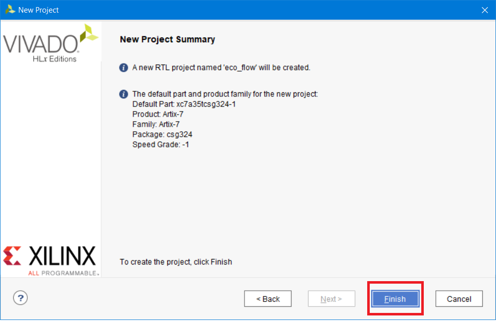
Figure 7 - The window of brief information of the created project
3.2. Creating and adding HDL files to a project
Here we will create two modules: just a flashing LED and a block memory that is constantly read (in fact, this is an imitation of the filter coefficient memory, the values of which we will try to change later).
To create and add a new file to the project, we will use the wizard, which is called by clicking on the blue plus (Fig. 8).
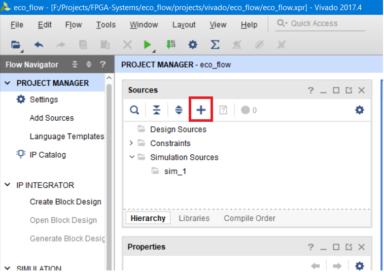
Figure 8 - Calling the wizard to create add files to the project
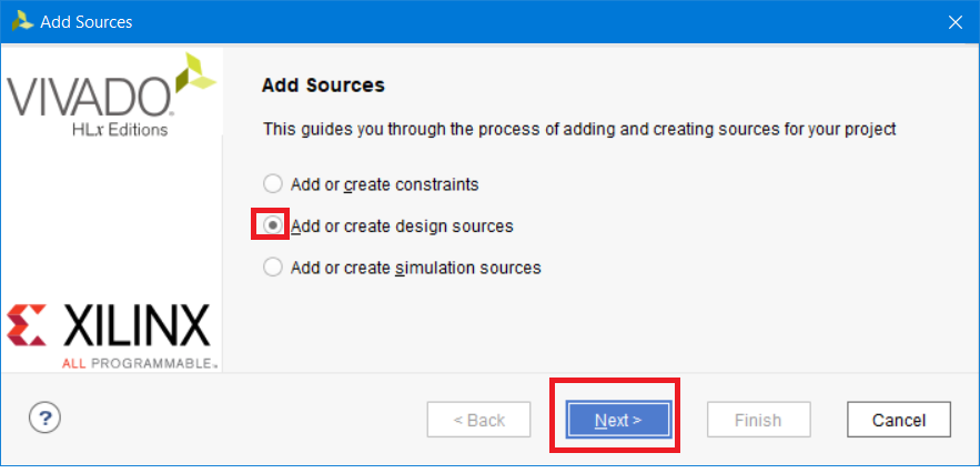
In the window that appears, select "Add or create design sources" and click Next (Fig. 9). Figure 9 - Selecting the type of file to be created or added
Select Create file, and then in the window that appears, in the File name field, enter the name of the flash_led file to be created, click OK (Fig. 10).
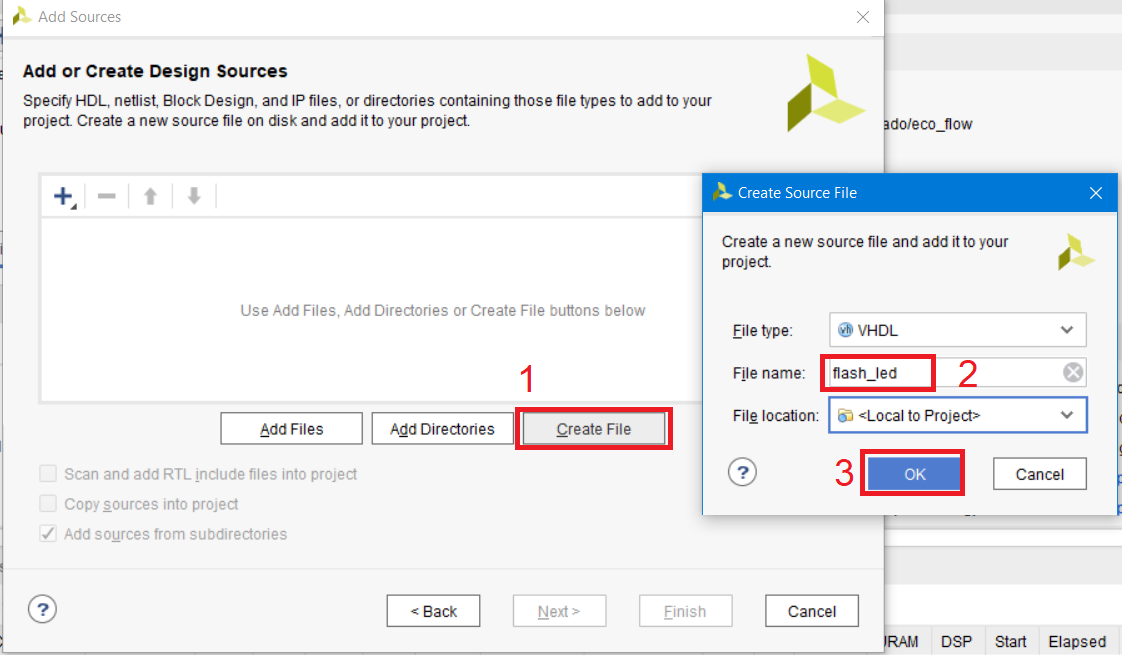
Figure 10 - Creating a new file and entering its name
After that, the file will appear in the list of added ones. Click Finish (Fig. 11)
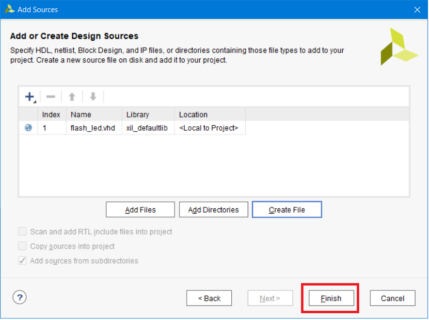
Figure 11 - List of added or created files
Now a wizard for creating a template for the file has appeared. Since I use VHDL, I can change the architecture name to rtl. We create two pins of our module: iclk with the “in” direction (clock signal of our module) and oled with the “out” direction (output connected to the LED). Click OK (Fig. 12).
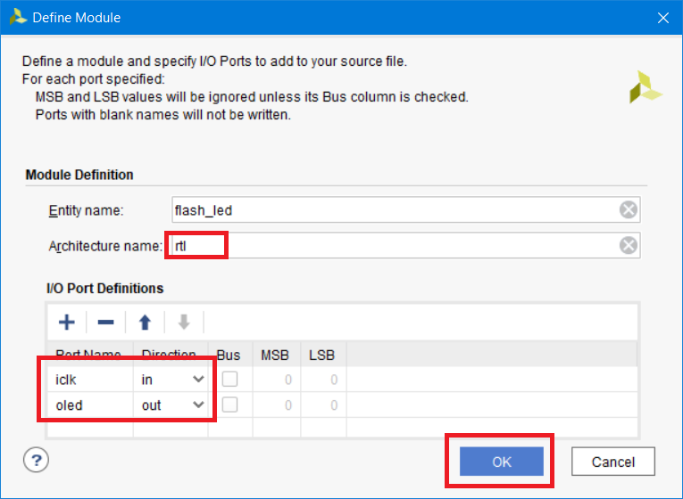
Figure 12 - Wizard for creating a module template (for VHDL)
Now our module is in the project tree (Fig. 13).
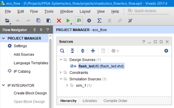
Figure 13 - The created flash_led module
The module should perform a simple function: just blink an LED with a period of 1 second. Looking ahead, I’ll say that the clock frequency of our project will be 100 MHz, and the module itself will still be useful to you when doing your homework.
Replace the contents of the file with the following (Listing 1 (for a text version of listing 1, see Appendix A)). The code is quite simple, and does not require additional comments to explain its work.
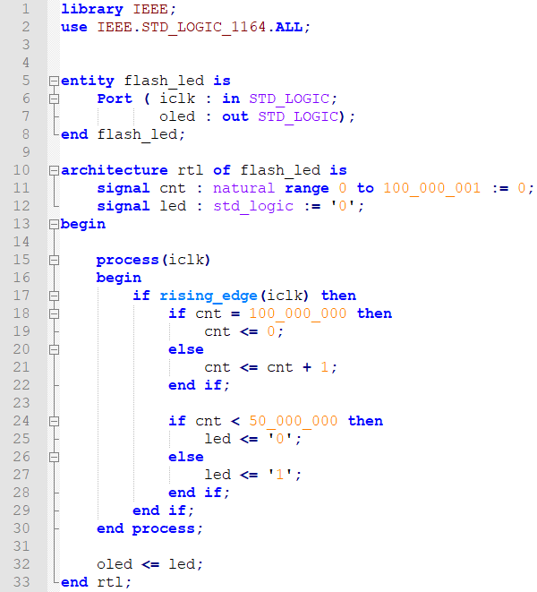
Listing 1 - Flash_led module code
Now create a new module, which should be called brom_reader, its iclk ports with the “in” direction, and odout [7: 0] with the “out” direction (repeat steps from Fig. 8 to Fig. 12).
If everything is done correctly, then the brom_reader module should appear in the project tree (Fig. 14).
Figure 14 - The brom_reader module in the project tree
Replace the contents of the module with the following text (Listing 2 (for the text version of Listing 2, see Appendix B)). A few comments will be required here:
- Line 13: an alias is created for the std_logic_vector type. Those who work with VHDL often use the "std_logic_vector ()" data type. In order not to write these long names every time, you can declare an alias and then use it throughout the module code.
- Lines 14-20: standard declaration of a two-dimensional array of natural numbers and initialization of the array (a memory with numbers is created).
- Line 22: using the alias slv to declare a signal
- Lines 23-24: use of the synthesis attribute [11]. Why is it registered here? We created a fairly small two-dimensional array (lines 15-20) - and most likely during synthesis it will be optimized and implemented as distributed memory on the LUT. And since we want to place the array in the block memory (BRAM-Block RAM), we need to explicitly tell the synthesizer about this, which is done using the synthesis attributes. Read more about them in the Vivado synthesis guide in [11].
Otherwise, everything should be clear: we created a ROM-memory from which its contents are continuously, sequentially and cyclically read.
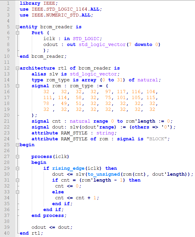
Listing 2 - brom_reader module code
3.3. Creating a MicroBlaze Project and Working in IP Integrator
Now we will create a project with MicroBlaze. Once again I draw your attention to the fact that there is a step-by-step guide in Russian on creating projects on the MicroBlaze software processor for beginners [16].
To create a block project, you need to create Block Design. Select Create Block Design, enter the name system and click OK (Fig. 15).
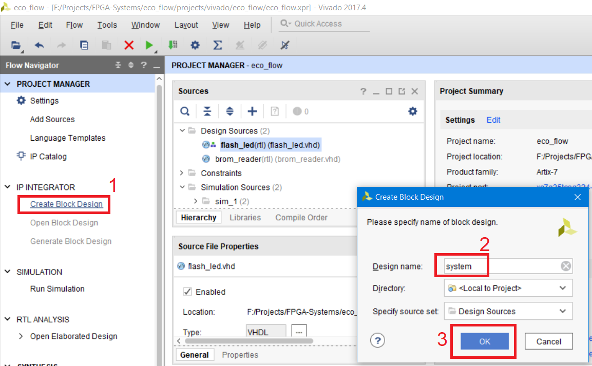
Figure 15 - Creating a new Block Design and setting its name
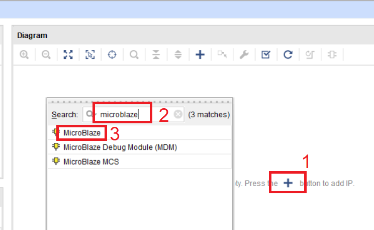
On the Diagram field, kernels from the Vivado IP directory, or RTL modules written in VHDL / Verilog / SystemVerilog are added. We will find the MicroBlaze module in the IP directory. To do this, click the blue X and enter “MicroBlaze” in the search field and select it (Fig. 16). Figure 16 - Adding the MicroBlaze IP core to the Diagram workspace
After adding MicroBlaze to the working field, we will use the express settings of the soft processor. Select Run Block Automation and set the settings according to fig. 17. Click OK.
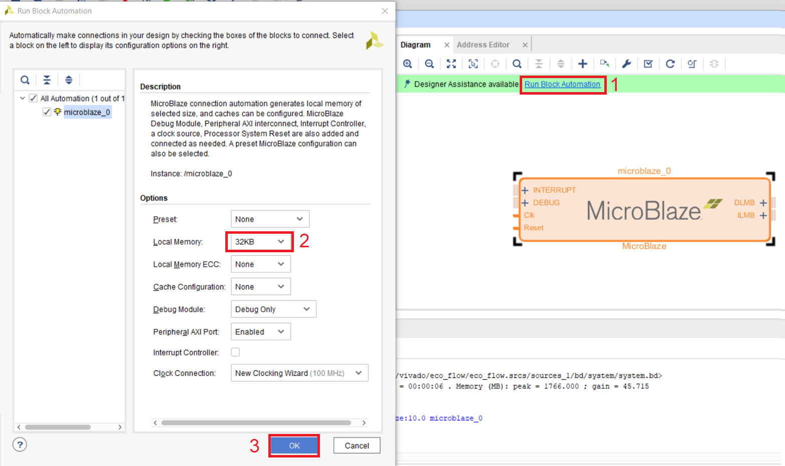
Figure 17 - Express settings MicroBlaze
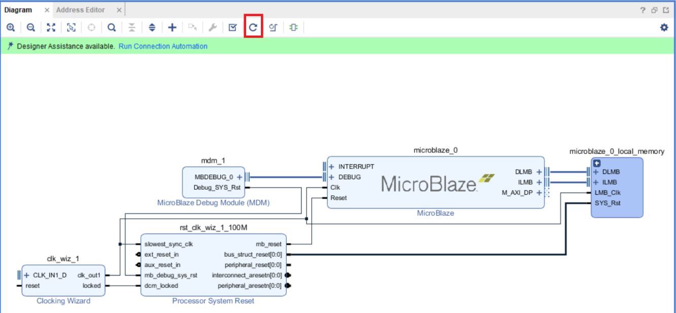
After that, several new IP cores will appear on the Diagram working field, including a clock generator and local processor memory [11, 12]. Press the Regenerate button to optimize the working field (Fig. 18). Figure 18 - Basic inclusion of MicroBlaze
Let's configure some modules in accordance with our Arty board. Set up the clk_wiz_1 clock grid generation module. To call the module settings, double-click on it with the left mouse button. In the settings window, set the value of the input clock frequency of 100 MHz, since the generator at 100 MHz is installed on the board [12]. We also set the source type as unipolar (Fig. 19). Let's go to the Output Clocks tab, where we will set the module output frequencies.

Figure 19 - Setting the parameters of the input frequency
In the Output Clocks tab, we will set only one frequency, the main frequency of our processor system and other modules. Set it to 100 MHz (Fig. 20).
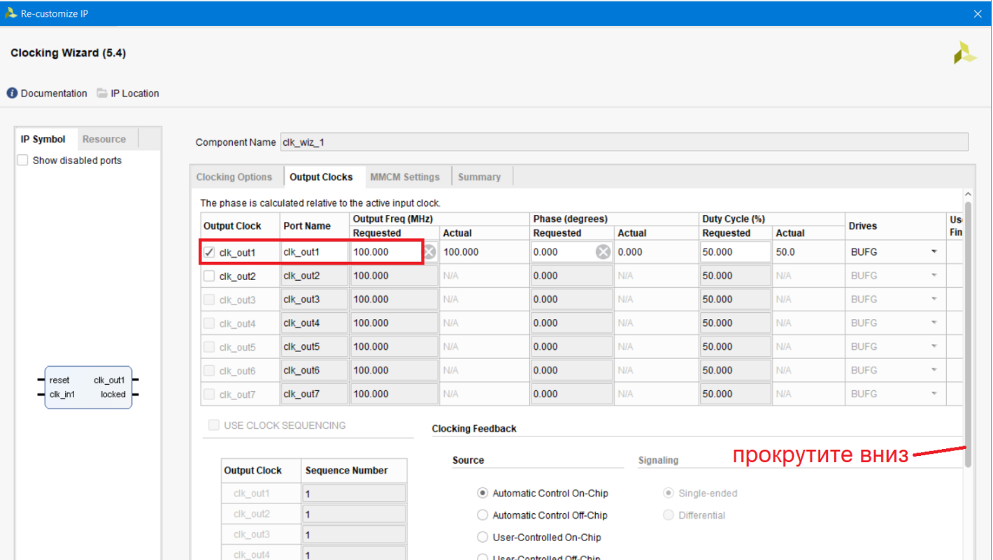
Figure 20 - setting the output frequency parameters
Scroll down to configure additional service tones. We will remove the reset signal, which we will not use. Uncheck it (fig. 21). We do not need the rest of the settings, click OK.
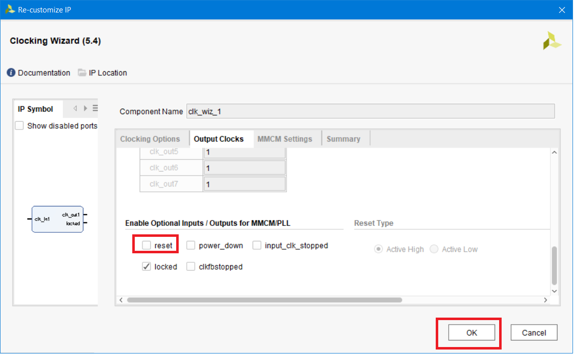
Figure 21 - Setting service signals
Now we declare the input clk_in1 of the module clk_wiz_1 external, in fact we make the input of our Block Design from it. To do this, click on clk_in1 with the right mouse button and select Make External (Fig. 22).
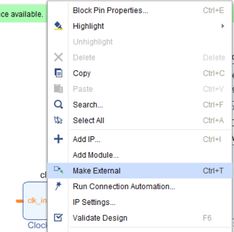
Figure 22 - Making the clk_in1 port external
As you can see, the clk_in1_0 port appeared (Fig. 23).
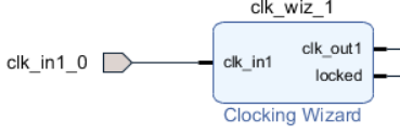
Figure 23 - Input port clk_in1_0
In the reset control module of our processor system, we connect two unused inputs (external reset and additional reset) to the inactive logic level “1”. We do this using an IP block called constant. To do this, click on the blue cross at the top, then in the search bar, enter “const” and select the constant module.

Figure 24 - Search for the IP block constant in the list of available IPs
Let's configure the module xlconstant_0 by double-clicking on it with the left mouse button. In the line value (Const val) we enter 1, in the line width (Const Width) we enter 1, click OK (Fig. 25)
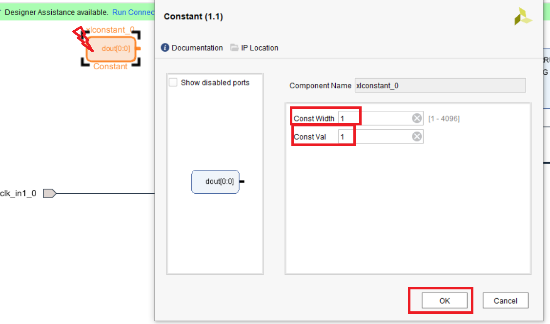
Figure 25 - Configuring the xlconstant_0 module
Connect the output dout of the module xlconstant_0 to the inputs ext_reset_in and aux_reset_in of the module rst_clk_wiz_1_100M. Just connect these ports with your mouse (fig. 26).

Figure 26 - Connecting unused ports to a constant
Add a UART module, finding it in the directory of available IP cores (Fig. 27). Figure 27 - Search for the UART module in the list of available IP blocks
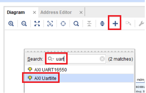
Let's configure the axi_uartlite_0 module by setting the transmission settings in accordance with Fig. 28. Then click OK.
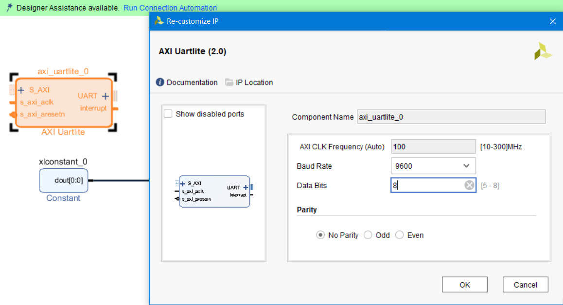
Figure 28 - Settings of the axi_uartlite_0 module
Now connect the axi_uartlite_0 module to the processor. We will use the automated method for this. Click on the top of Run Connection Automation and select what to connect to (AXI UART input to AXI MicroBlaze) fig. 29.

Figure 29 - Connecting axi_uartlite_0 to the processor
The UART interface is standard and separated into a separate type of interface in Vivado IP Integrator. In paragraph 2 of Fig. 29 we said that we want to make the rx and tx of the axi_uartlite_0 module external. If you open the interface, you will see it. Do not be embarrassed that there is only one blue wire in the interface, later, when we create the HDL wrapper for the project, you will see that there are two ports (rx and tx).
Click the Regenerate Layout button. After that, the Block Design workspace will be optimized and the circuit will accept the id, as in Fig. 30. Make sure that you are connected correctly. If everything is normal at this stage, continue, if there are errors, rebuild the processor system.
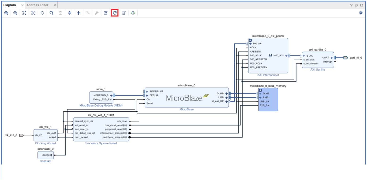
Figure 30 - The intermediate stage of assembly of the processor system.
Let's add another module to the AXI bus. This will be the GPIO module, the output of which we will connect to the LED. Find the AXI GPIO module in the list of available IP blocks and add it to the working field (Fig. 31). Figure 31 - AXI GPIO module in the list of available IPs

Configure the module in accordance with fig. 32 (we will use only one channel and one output).
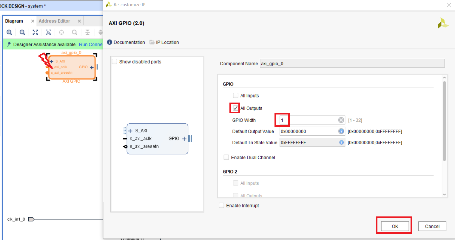
Figure 32 - Settings of the axi_gpio_0 module
Connect the axi_gpio_0 module to the processor and make the output external. Click Run Connection Automation and check all the boxes (fig. 33).

Figure 33 - Connecting axi_gpio_0 to the processor
Click the Regenerate Layout button and make sure all connections are as shown. 34.
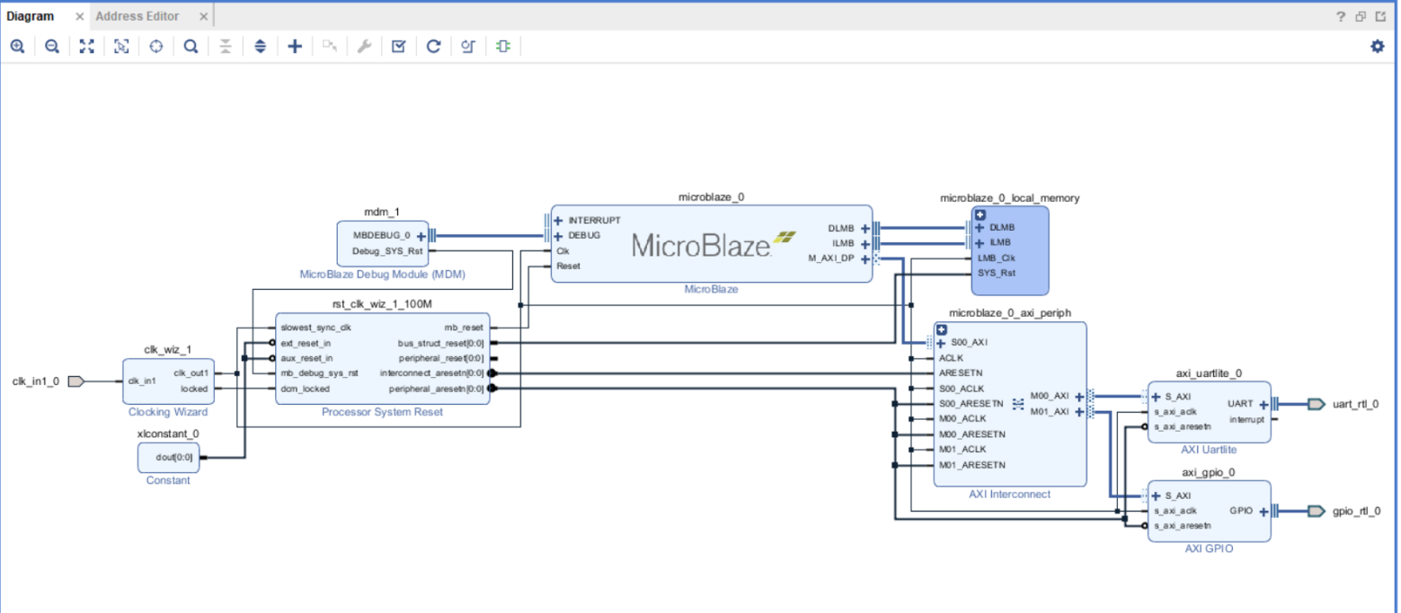
Figure 34 - Assembly of the processor system.
Now add the debug module ILA. Suppose we want to view transactions on the AXI Lite bus for the UART module. We find in the list of available IP modules ILA (Integrated Logic Analyzer) Fig. 35. Figure 35 - IP block ILA in the list of available
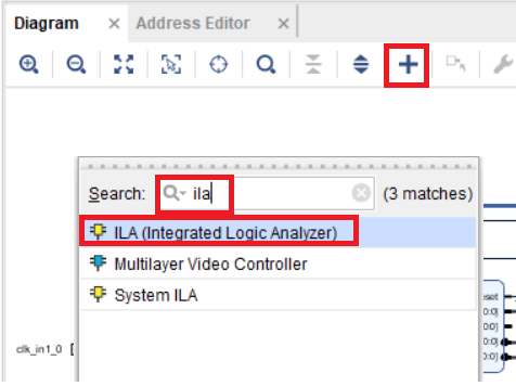
Here we use some similarity to the so-called HDL Insertion Flow, when we add debug modules directly to the HDL code. Let me remind you that you can also search for circuits for debugging in netlist after synthesis. This approach is called Netlist Insertion Flow.
Since we want to debug AXI transactions, we must configure the ILA probe type as AXI (Monitor Type parameter in the ILA block). This mode is set by default, so just connect the input SLOT_0_AXI of the ila_0 block to the AXI bus, the transactions on which we want to view. In our case, this is a bus going from the interconnect to the axi_uart_0 module (Fig. 36). We also connect the clock signal for the module to the clk of our system and click the Regenerate Layout button.

Figure 36 - Connecting ila_0 to the AXI bus axi_uart_0
By default, the length of the recorded data is set to 1024, which is enough to view the transaction.
Now add our RTL modules to Block Design, for this select the flash_led module, right-click and then select Add Module to Block Design (this only works in Vivado no lower than version 2017.1).
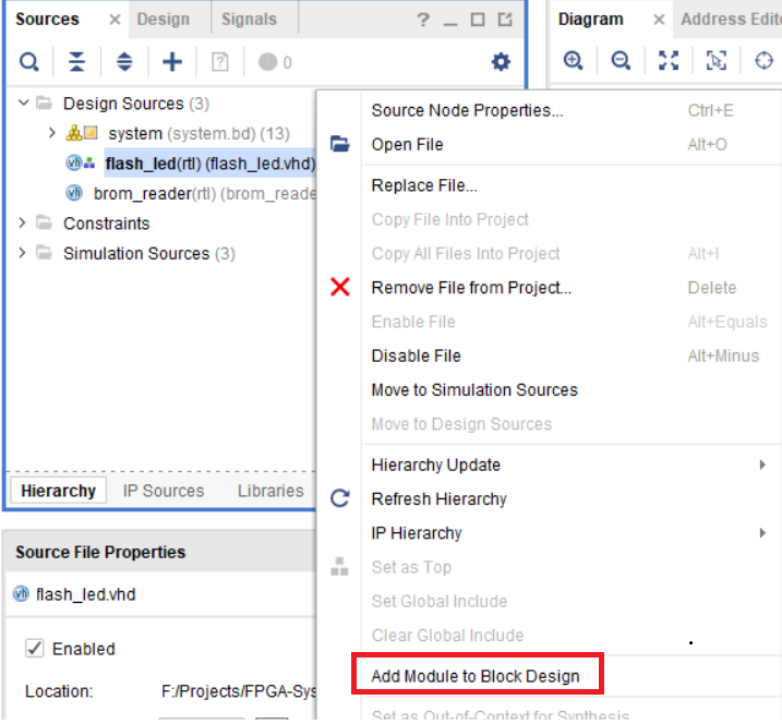
Figure 37 - adding flash_led module to the Diagram field
Connect the iclk input of the flash_led_0 module to the clock of our system, and make the oled port external (right-click on the port, then select Make Exernal). Click the Regenerate Layout button.
If everything is done correctly, then it should turn out as in fig. 38.
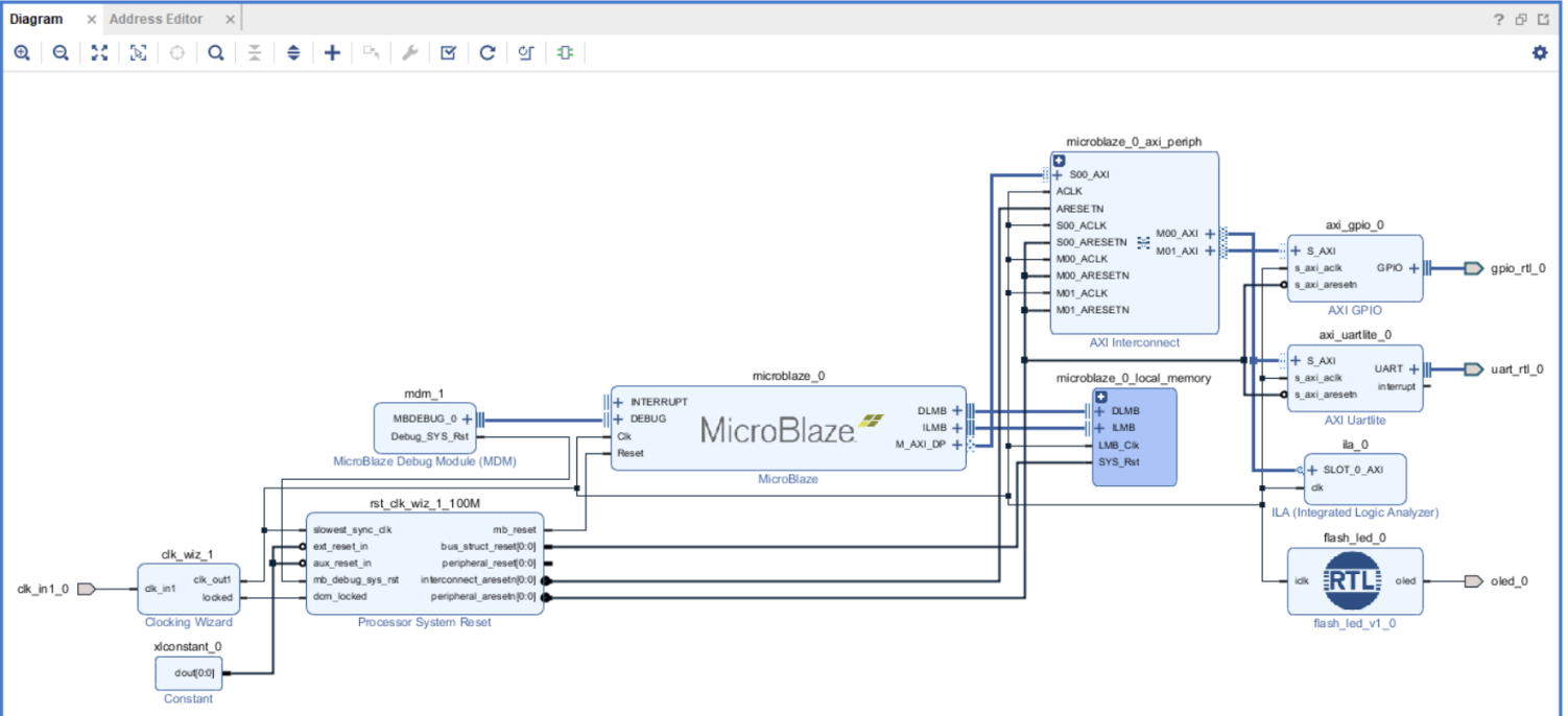
Figure 38 - The intermediate stage of building a project in IP Integrator
Repeat the same steps to add the brom_reader module. Connect its iclk clock input to the clock circuit, BUT do not declare the odout [7: 0] output external. Click Regenerate Layout. If everything is done correctly, then it should turn out as in fig. 39.
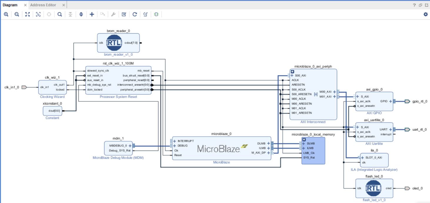
Figure 39 - The intermediate stage of building a project in IP Integrator
Now, add another ILA and connect it to the output odout [7: 0] of the brom_reader_0 module.
We find the ILA IP block in the list of available ones (Fig. 35) and add it to the Diagram field. Let's configure it by double-clicking on it with the mouse. Set Monitor Type to Native (we are not debugging the AXI bus, but simple circuits). Leave the rest by default. Go to the tab Probe_Ports (0..7) fig. 40.
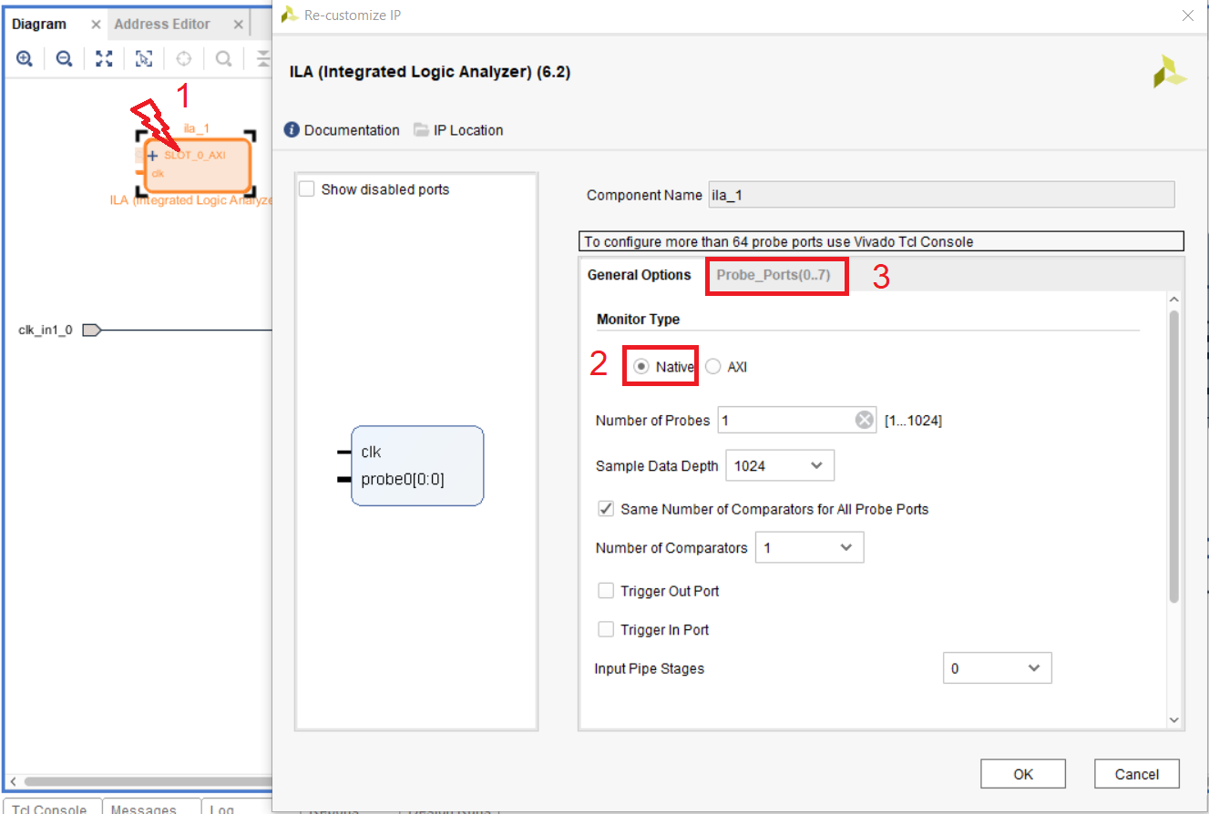
Figure 40 - Configuring ILA
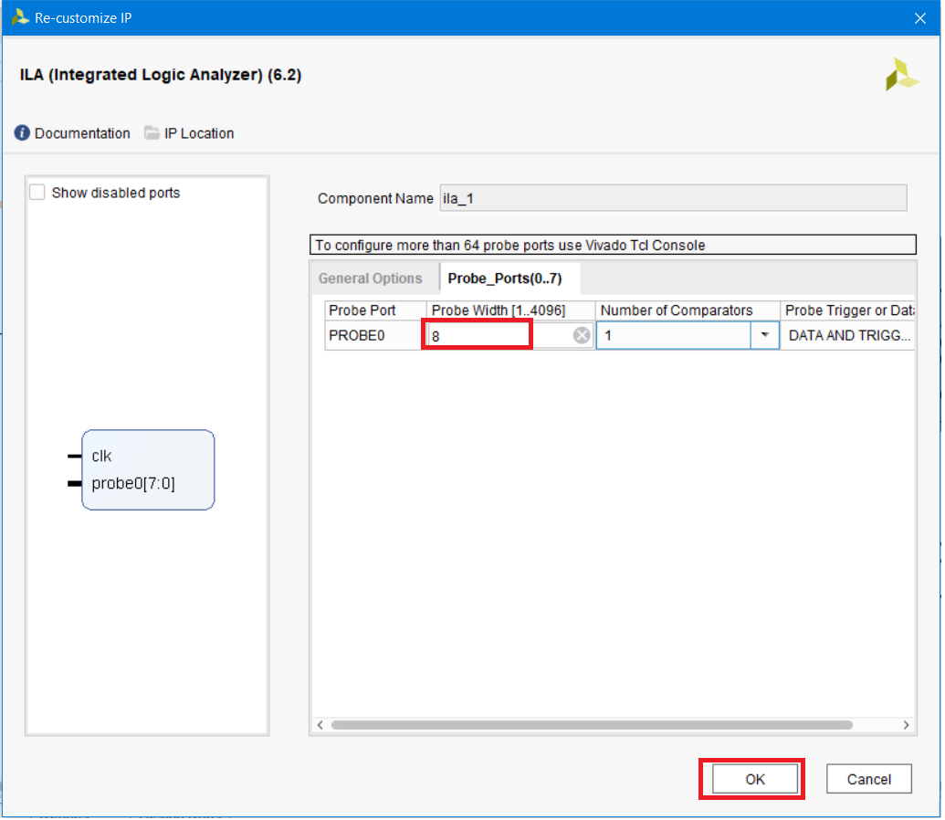
Let's adjust the probe width. We set the width value to 8 (Fig. 41), since it is 8 bits - the width of the output bus odout [7: 0] of the brom_reader_0 module. Click OK. Figure 41 - ILA probe width setting
Connect the output odout [7: 0] of the brom_reader_0 module to the probe_0 [7: 0] input of the ila_1 module, and connect the clk input of the ila_1 module to the clock circuit of our project. Click the Regenerate Layout button, and if everything is correct, it should turn out as in fig. 42.

Figure 42 - An intermediate stage of building a project in IP Integarator
It remains only to add a button and the LED turned on directly with it.
Create an input port by right-clicking on an empty spot in our block diagram and selecting Create Port (Fig. 43).

Figure 43 - Creating a port in IP Integrator
After the port settings wizard appears, enter its name ibtn, specify the direction input and, if necessary, bit depth. Click OK (Fig. 44).
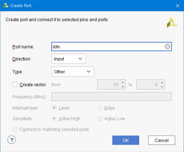
Figure 44 - New port setup wizard (ibtn button)
After that, the port will appear on the Diagram field (Fig. 45).

Figure 45 - created ibtn port
Create another port called obtn_led, with the output direction (repeat the steps in Figure 43-44).
Now just connect the ibtn port to obtn_led, click Regenerate Layout. It should turn out as in fig. 47.
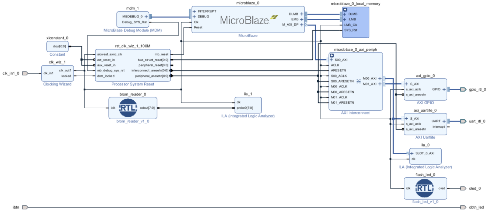
Figure 46 - Assembled project in IP Integrator
Check that there are no errors in the current Block Design by clicking on the Validate Design button. If everything is correct, but Vivado will display a message. Click OK and save the current Block Design (Fig. 48).
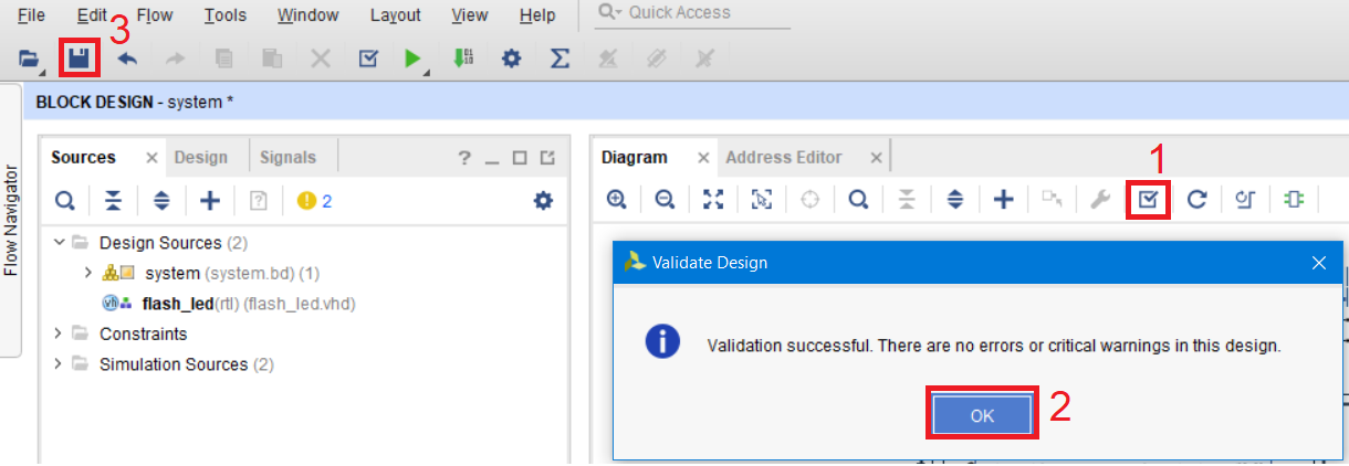
Figure 47 - Validation of the assembled project in IP Integrator
3.4. Synthesis and implementation
Go to the Sources tab, right-click on system and select Create HDL Wrapper (create HDL wrapper of our Block Design) fig. 48.
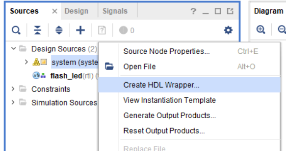
Figure 48 - Creating a project wrapper
After that, Vivado will offer to either manually update the HDL wrapper when making changes to Block Design, or do it automatically. We leave the automatic update and click OK (Fig. 49).
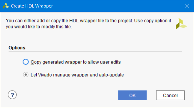
Figure 49 - HDL wrapper update options
Now we indicate that the system_wrapper module is the Top module. Right-click on system_wrapper and select Set as Top (Fig. 50).
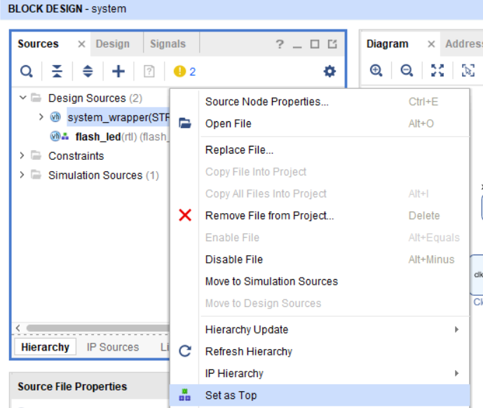
Figure 50 - Making the system_wrapper module the top module
Now we will perform the synthesis of the system_wrapper module by clicking on the Run Synthesis button (Fig. 51).
Note: to connect debugging blocks, we actually used HDL Insertion Flow [4], that is, we actually inserted our ILA blocks into the code and connected the chains to them. It makes no difference how you create and connect debugging chains: via HDL or Netlist. Ultimately, ECO works with synthesized or implemented netlist, which is stored in Design Checkpoint.
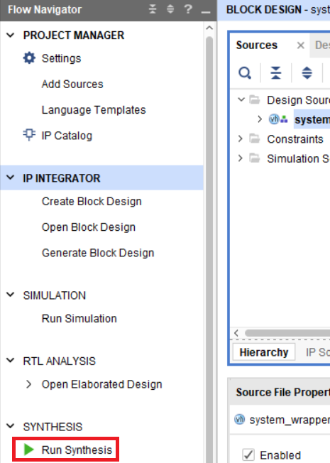
Figure 51 - Starting the synthesis of the project
After clicking on the Run Synthesis button, click OK and wait for the synthesis to complete.
After the synthesis is completed, a window will be displayed in which you will be prompted to start the implementation, open the synthesis results or view the reports. Open the synthesis results (Fig. 52).

Figure 52 - Opening the synthesis results
Now connect the legs in our project. This is done using Pin Planer. To open it, click Window → I / O Ports (Fig. 54).
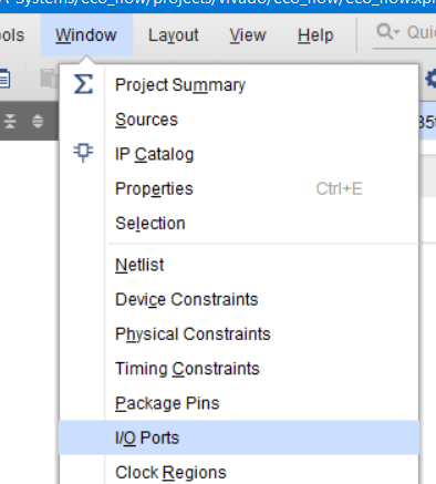
Figure 53 - Opening the window for assigning pins
Using the Reference Manual [12] for Arty, assign the legs (Fig. 54).
BE CAREFUL!!! I specifically mixed up the legs for the rx and tx of the UART module!
Assign legs according to fig. 54.
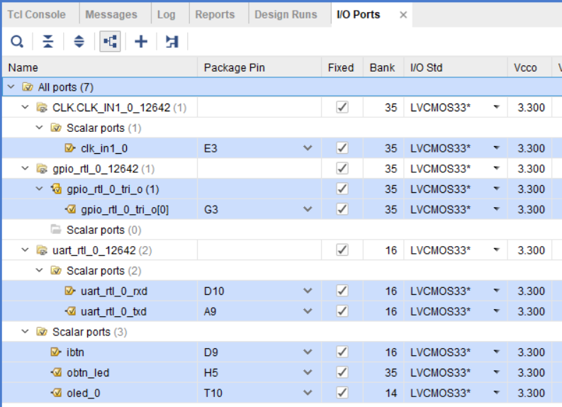
Figure 54 - Assignment of project legs (rx and tx UART are mixed up specially)
Click the save button, after which Vivado will indicate that you did not create the project constraint file and prompt you to create it. Enter the name of the constr file and click OK (Fig. 55).
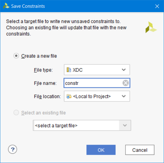
Figure 55 - Creating a design constraint file
Now we can implement our project and generate the firmware file. Press the Generate Bistream button, then OK and wait for the procedure to complete (Fig. 56).

Figure 56 - Location of the Generate Bitstream Button
After the Bitstream generation is completed, a window for further actions will appear. Click Cancel (Fig. 57)
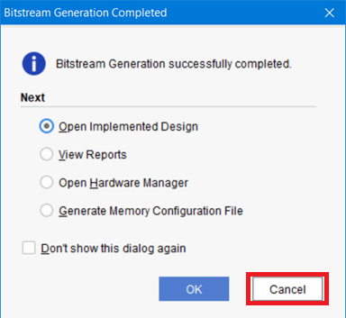
Figure 57 - The window for further actions after the creation of the bitstream
3.5. Writing a program for MicroBlaze
Now let's do the software development for MicroBlaze. This is done in the Xilinx Software Development Kit (SDK) environment. In order to inform the SDK of information about the assembled processor system (IP cores, their addressing on the AXI bus), it is necessary to export to the SDK. This is done using File → Export → Export Hardware (Fig. 58).
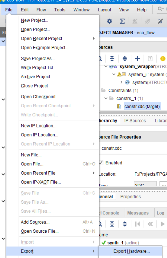
Figure 58 - Export processor system information to the SDK
In the window that appears, do not check the Include Bitstream checkbox. Leave the default settings and click OK (Fig. 59).
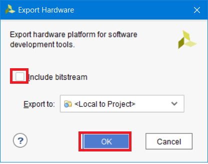
Figure 59 - Export options window
Now run the SDK. To do this, select File → Launch SDK
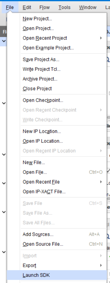
Figure 60 - Launch SDK
Wait for the SDK overhead to complete. After their completion, we can begin to create a new project. Choose File → New → Application Project.
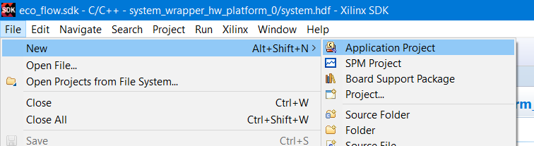
Figure 61 - Creating a new project in the SDK
Enter the name of the new MB_run project, click Next (Fig. 62)
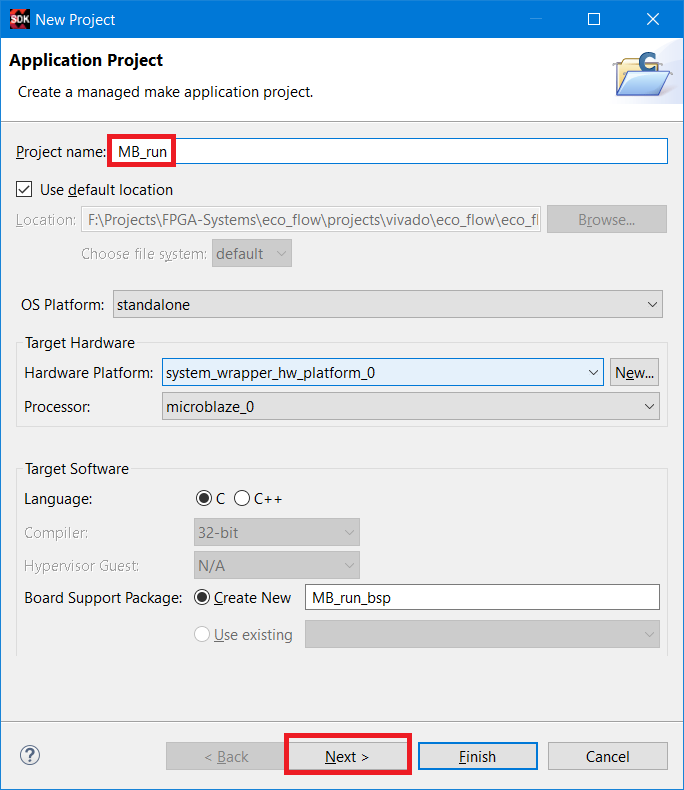
Figure 62 - Setting up a new project
In the ready-made templates window, select the Hello World application creation and click Finish (Fig. 63)
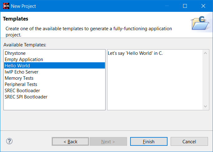
Figure 63 - Selecting a template for a created project
Open the helloworld.c file (the location of which is shown in Figure 64) and replace its contents with the program code shown in Listing 3 and save the result.
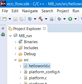
Figure 64 - Location of the helloworld.c file
Listing 3 - Replaced contents of the helloworld.c file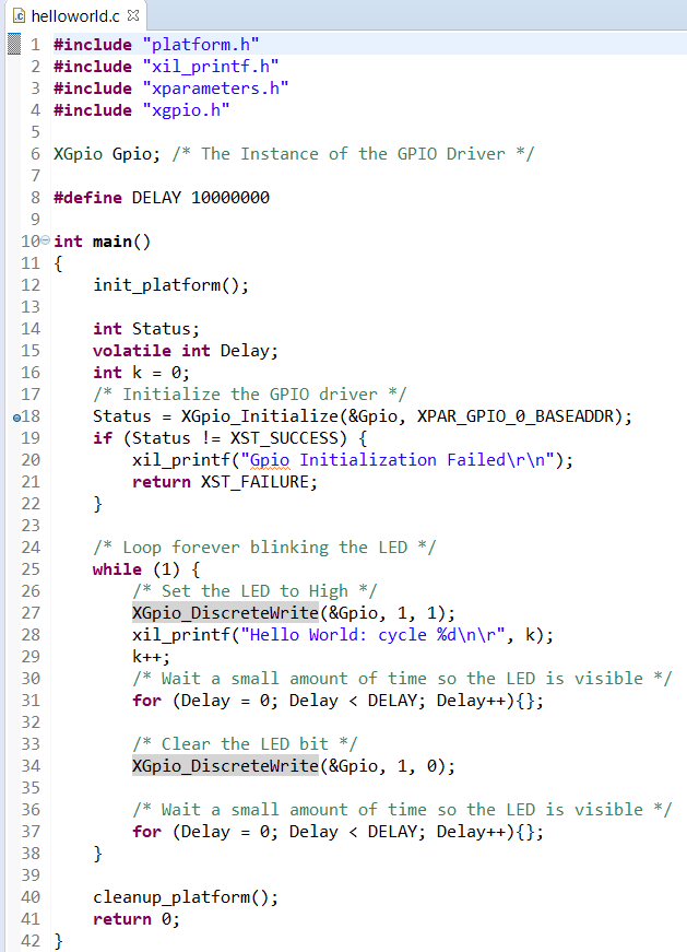
The program sends “Hello World: cycle” about 1 time in 2 seconds and blinks the LD1 LED (red component) also about 1 time in 2 seconds.
3.6. Run the program and debug
After completing the code writing and assembly of the processor system, you must make sure that:
- LD4 LED lights up when BTN0 is pressed
- The processor works and sends “Hello World: cycle” to the console, however we do not see words in the console, because we made the wrong connection rx and tx. An additional indicator of processor operation is the flashing LD1 LED.
- AXI-Lite transactions are performed from the processor to UART
- Block memory is read and returns the correct values.
First, connect Arty to the computer. Let's configure the terminal in which UART messages should be displayed. This can be done using standard SDK tools. The SDK has a terminal located below (Fig. 65).
If there is no terminal, then it can be found in Window → Show View → Others → Xilinx → SDK Terminal (Fig. 65).
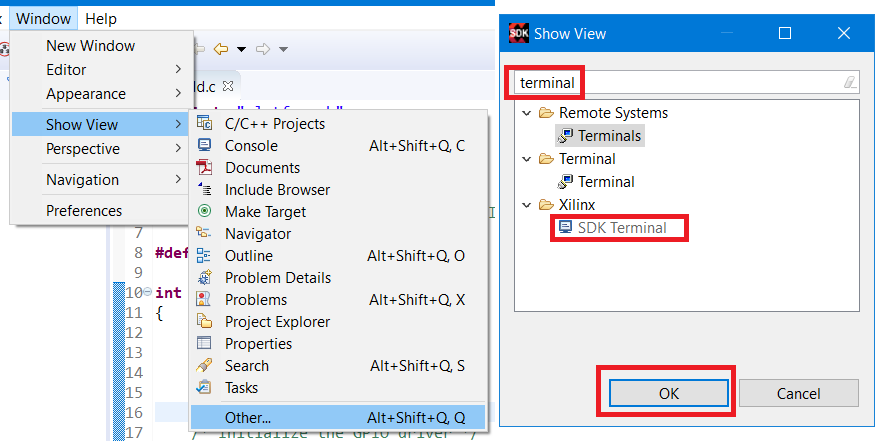
Figure 65 - Opening the embedded terminal in the SDK
Set the terminal settings in accordance with fig. 66. The COM port number may vary.

Figure 66 - Configuring the terminal SDK
Now let's move to Vivado and do the FPGA programming.
Click Open Hardware Manager and go into programming and debugging mode. Select Open Target and click on Auto Connect (Fig. 67)

Figure 67 - Opening Hardware Manager and connecting to the FPGA
Select our crystal from the list and fill it with firmware (Fig. 68)
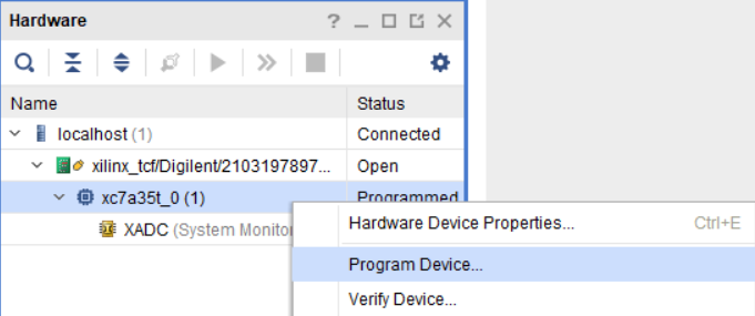
Figure 68 - FPGA Programming
In the dialog that appears, check that the desired .bit firmware files and the list of .ltx plug-in circuits are selected (Fig. 69) and then click the Program button.

Figure 69 - Selecting the firmware file and the list of circuits
If everything is done correctly, the LD4 LED should blink, and by pressing the BTN0 button, the LD4 LED should light up.
Now we make the processor execute our program for sending data to UART and blink the red component of the LD1 LED.
Switch back to the SDK, right-click on our MB_run project, and then select Run As → Launch on Hardware (System Debugger), as shown in Fig. 70. We immediately upload the program release, and we will not perform step-by-step debugging.
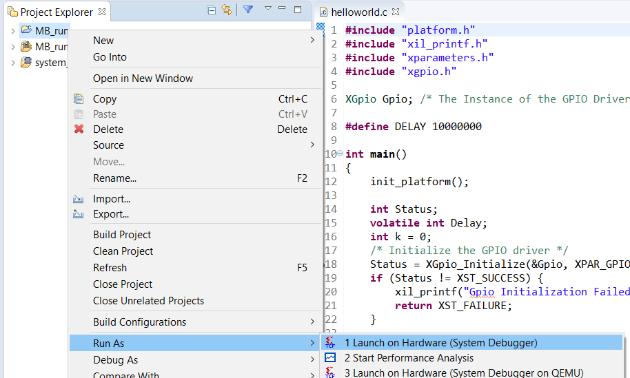
Figure 70 - Starting the processor executable program
After waiting a few seconds, we see that the LD1 LED is blinking, but messages in the SDK Terminal do not appear, because rx and tx are mixed up.
Now let's make sure that transactions reach the UART module.
Switching to Vivado. I hope that you remember that we connected two ILAs: one for a transaction on the AXI bus for UART, and the other for block memory output. But we had three ILAs in our list (Fig. 71).

Figure 71 - Connected ILA window
Unfortunately, as a result of optimization and synthesis, this can happen and this should be taken into account, as well as the fact that as a result of optimization and various synthesis settings, the names of the chains can change. Nevertheless, we can debug and make sure that transactions still reach the UART module. But we need to “catch” them, that is, configure the trigger, the condition by which the state of the lines to which the ILA is connected will begin recording.
Double-click hw_ila_1 to open the timeline window and the settings window.
In the Trigger Setup window, set the trigger. Click on the blue cross and in the list of available chains select the chain shown in fig. 72. And click OK.
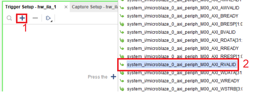
Figure 72 - Selecting a trigger to trigger ILA
Note: we work with the AXI-Lite interface, in which there are a lot of signals. I will not describe here the functions that are assigned to certain interface signals. If you are interested in learning more about this, please refer to the manual [14].
Now set the trigger parameters. Since the active level of the RVALID signal is “1”, we say that it is necessary to start recording when this signal is equal to “1”. Set the trip value as shown in fig. 73. And then press the trigger trigger button.

Figure 73 - Recording data from the ILA on the trigger
Now, from this giant list of circuits that are available in the interface, we find the bus that is responsible for the data. This tire is shown in fig. 74
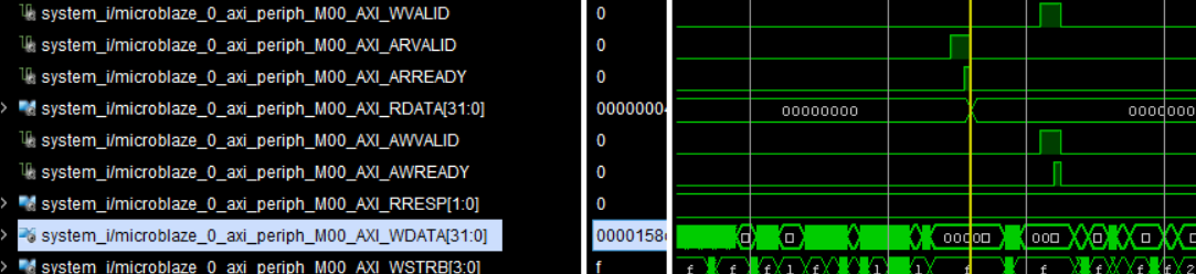
Figure 74 - Data circuit on the AXI-Lite bus
Change the displayed bus status to ASCII. To do this, right-click on the bus, then select Radix, then ASCII (Fig. 76).

Figure 75 - Selection of data representation on the * WDATA bus [31: 0]
After that, we will see on the bus part of our message that the processor sends. This partially confirms that the transaction is proceeding correctly (Fig. 76).

Figure 76 - ASCII representation of data on the * WDATA bus [31: 0]
Try to repeat the steps from fig. 71 to fig. 76 for hw_ila_2, which is connected to the output of a block memory reader. A trigger is not required. If everything is done correctly, then the picture should be similar to fig. 77.
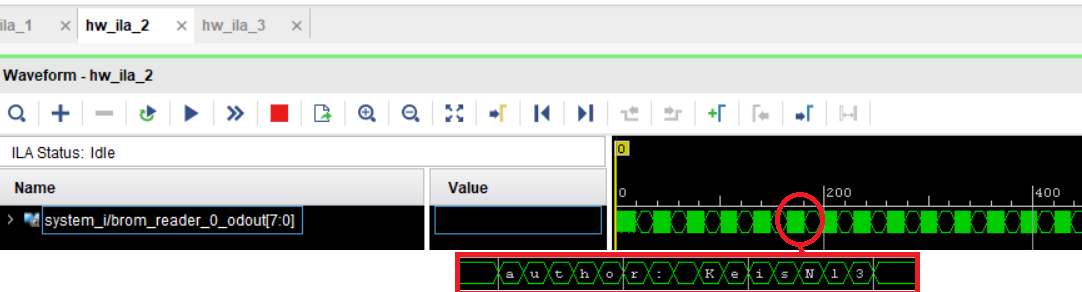
Figure 77 - Data Read from Block Memory
This completes the assembly of the test project, and we can begin to edit our netlist and work in ECO mode.
4. Switch to ECO mode
As we saw above:
- By pressing the BTN0 button, the LED lights up
- UART packages are sent, but we do not see them in the console (rx and tx are specially mixed up)
- The contents of the block memory are read cyclically and continuously (the contents of the block memory in ASCII: ”author: KeisN13”).
To fix errors, edit netlist and change the content and functionality of some components, we will use the ECO mode, which is available when working with Design Checkpoint (DCP). We will use DCP, which is obtained after the phase of the crystal trace (post route).
Each time you run a new synthesis or implementation, Vivado deletes DCP, so the common practice of working with DCP is to copy-paste the necessary DCP to a new directory.
Let's create the edited_dcp folder. I will create it next to the project folder (Fig. 78)
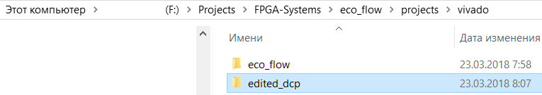
Figure 78 - Creating a folder for saving DCP
We copy the DCP file necessary for further work, which is located “project_folder / project_name.runs / implementation_name / top_module_routed.dcp name” (Fig. 79) into the edited_dcp folder.
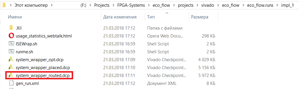
Figure 79 - DCP location
Go to Vivado and open the DCP. To do this, click File → Open Checkpoint (Fig. 80)
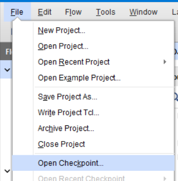
Figure 80 - Opening DCP
Select the location of the copied DCP file in the edited_dcp folder and click OK.
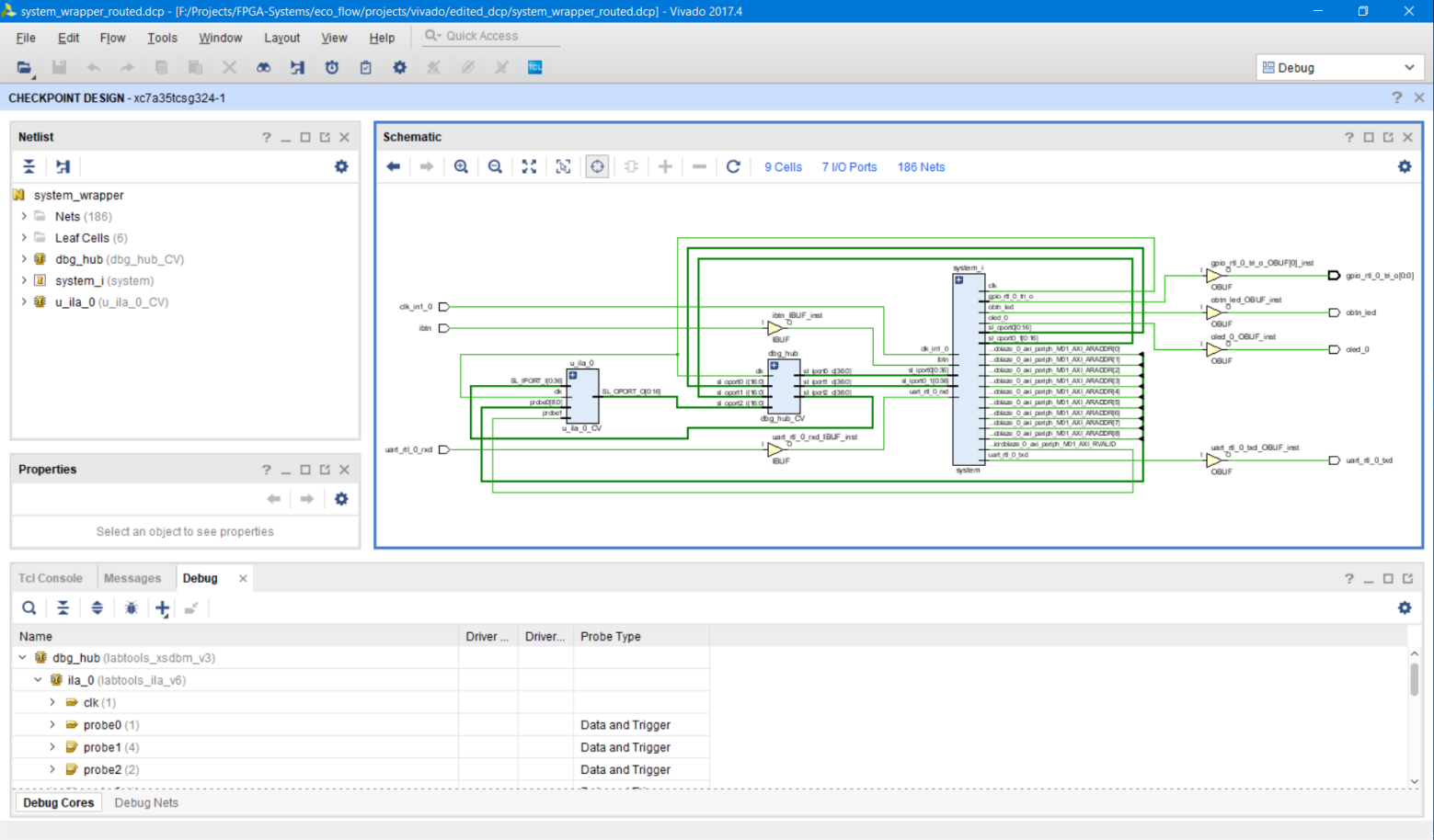
After opening DCP, by default, the Default (or perspective) view will open, the one you used the last time you opened DCP (Fig. 81). Figure 81 - Vista Debug open DCP
There are several modes of operation with DCP, however, today we are interested in ECO Flow. To switch to ECO mode, you need to change the view. To do this, select ECO in the upper right corner from the drop-down list (Fig. 82).
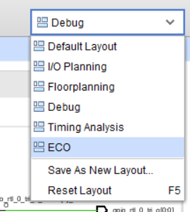
Figure 82 - Switching to ECO mode
As you can see, the graphical representation changed when switching to ECO mode (Fig. 83). New controls and a graphical interface have appeared, which we will consider further.

Figure 83 - Presentation in ECO mode
5. ECO: interface description
Work in ECO mode has its own route, which is shown in Fig. 84. All work is done in the appropriate DCP. After opening DCP, the necessary changes are made to the netlist using the GUI tools and / or Tcl commands. Changes are saved, and, depending on whether the project is already fully placed in the crystal or not, placement and tracing are performed, or only tracing. Then the crystal is wired, after which new firmware files (bitstream, .bit) and logic analyzer circuits (.ltx) are generated. The next step is to verify the changes made "in hardware", and if everything is fine, then the changes made are made to the original project. If not, then the changes to the DCP can be repeated.
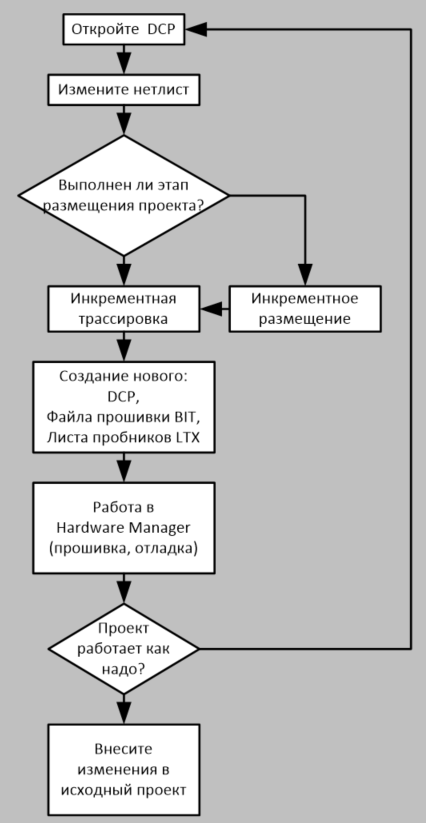
Figure 84 - Design route in ECO mode
Making changes is possible using the GUI tools. The original description of the interface can be found in [3] in the Vivado ECO Flow section.
The graphical representation in ECO mode is divided into several sections, the location and purpose of which are identical to the standard representation in which the main design is carried out.
On the left side of the screen is the ECO Navigator, which presents tools for the design route. ECO Navigator consists of several sections.
Section Edit (Fig. 85): provides access to the tools necessary for editing netlist

Figure 85 - Edit section commands
Create Net: Opens a dialog box that provides access to create new circuits. Chains can be created for any level of the hierarchy by specifying the hierarchy name in the chain name. Tires can be created. If pin or port is selected, then the circuit can be automatically connected to them if the Connect selected pins and ports checkbox is installed (Fig. 86).
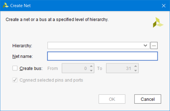
Figure 86 - Create Net Dialog Box
Create Cell: opens a dialog box that allows you to add additional components to the current netlist. It is also possible to create cells in the required hierarchy level. You can create as library components that are available from the list, or black box. If you create a LUT, you can immediately edit the function that it should implement (Fig. 87).
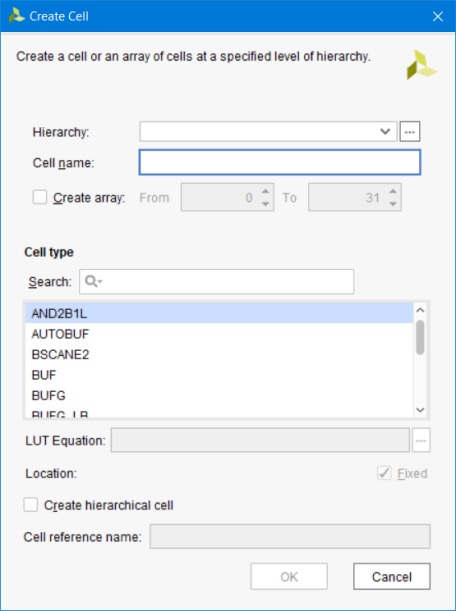
Figure 87 - Create Cell Dialog Box
Create Port: calls the wizard to add and configure additional ports to the current netlist. It is possible to configure several parameters: direction, bus width, voltage standard, etc. (Fig. 88).
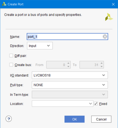
Figure 88 - Create Port Dialog Box
Create pin: Adds and configures pins in the current netlist. A pin can be created for the current cell (objects of type cell) at any level in the hierarchy. A pin for a top-level hierarchy can also be created using the create_port command. A pin cannot be created if the cell and the name of the created pin are not specified (Fig. 89).
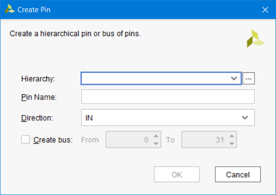
Figure 89 - Create Pin Dialog Box
Connect Net: Connects the circuit to the selected pin or port. The dialog box that opens allows you to view the list of circuits or search for them. The selected chain will be connected through all levels of the hierarchy, automatically creating the necessary pins.
Disconnect Net: Disconnects the selected circuit, pin or port from the circuit. If an object of type cell is selected, then all circuits connected to it will be disconnected.
Replace Debug Probes: allows you to call up a dialog box in which it is possible to edit the ILA and / or VIO (Virtual Input Output) ports that were created earlier, that is, disconnect the current circuits from and connect new ones.
Place Cell: allows you to place an object of type cell in the selected crystal resources.
Unplace Cell: removes the selected object of type cell from the current location.
Run Section
Commands of the Run section provide access to all the commands needed to complete the implementation.
Check ECO: Runs error checking (DRC - Design Rule Check)
Note: Vivado allows you to make many changes to the netlist using ECO mode commands. However, the logical changes introduced into the project can lead to unrealizable physical implementation. The launch of Check ECO should be done before you are planning to implement the project in order to eliminate errors in the early stages of the ECO Flow route.
Optimize Logical Design: in some cases, it is recommended to perform netlist optimization using the opt_design command and its corresponding options [9]. Optimize Logical Design allows you to call up a dialog box that allows you to enter the appropriate Tcl arguments to the opt_design command, which are set in the options line.
Place Design: Performs incremental (i.e. based on previous netlist) placement of components of the current netlist. The Incremental Placement Summary report, which is displayed in the console at the end of the place_design command, allows you to view statistics on the reuse of the results of the previous placement, which was in the original DCP before the changes were made. Clicking on Place Design brings up a window in which the corresponding options for the place_design [9] command can be set. For more information about incremental implementation, see [3] in the Incremental Compile section.
Optimize Physical Design:in some cases, it may be necessary to perform physical optimization (phys_opt_design [9] command). The dialog box called up by clicking on Optimize Physical Design allows you to enter the appropriate options for the phys_opt_design command.
Route Design: opens a dialog box that allows, depending on the choice, to perform incremental tracing of the changes made to the netlist, tracing of the selected pins or circuits. If the percentage of reused corroded chains is less than 75%, then a normal netlist trace will be generated.
For more information about incremental implementation, see [3] in the Incremental Compile section.
Report Section
In this section, it is possible to generate the necessary reports for the changed netlist, including a report of the resources used, time characteristics, intersection of clock domains, etc.
Program Section The
tools of this section allow you to save the changes made to the new DCPs, create the FPGA firmware file, create a new list of debugged circuits through ILA, in case the ILA has undergone changes, program the FPGA and perform debugging using standard Vivado Hardware Manager tools.
Scratch tab
Allows you to track changes made to the netlist, including viewing and connecting unused pins, ports, circuits. The connection column Con monitors the connection status of objects, PnR monitors the status of placement and tracing of objects.
By clicking on the changes with the mouse on the Scratch tab, a menu of additional actions will be called up (Fig. 90). The functionality that they perform, I guess, is intuitive based on their names. A complete list and actions that the commands execute are given in [3] in the section Vivado ECO Flow → Scratch Pad → Scratch Pad Pop-up Menu.

Figure 90 - The menu of additional actions of the Scratch tab
6. Modification of the project
Now we can begin to make changes to our project. The first thing we will do is install the new component in a netlist. We make the LD0 LED light up, and when you press the BTN0 button, it goes out. In other words, we must insert an inverter into the netlist, which is not there.
6.1. Creating new elements in netlist
First, find the ibtn port in the diagram, left-click on it once, and then press F4. Thus, we will try to filter out all unnecessary in the schematic, to increase the readability of netlist.

Figure 91 - Opening the schematic for the selected port
In the window that appears, we will see only one ibtn port. Now we will display the entire circuit from the ibtn port to the LD1 LED (obtn_led port). Right-click on the ibtn port, then Expand Cone and select To Flops or I / Os. And press the Regenerate Layout button (Fig. 92)

Figure 92 - Display of the endpoints to which the port is connected
Now we see the full “path” from the button to the LED (Fig. 93).

Figure 93 - “Path” from ibtn port to obtn_led
The next step that needs to be done is to decide where to break the chain. I suggest breaking it from the system_i module to the output buffer. To do this, select the chain from the obtn_led pin of the system_i module to the I pin of the obtn_led_OBUF_inst buffer, then in the Edit section, select Disconnect Net.

Figure 94 - Selection of an open circuit
After clicking on the Regenerate Layout button, we see that the circuit has been removed (Fig. 95)
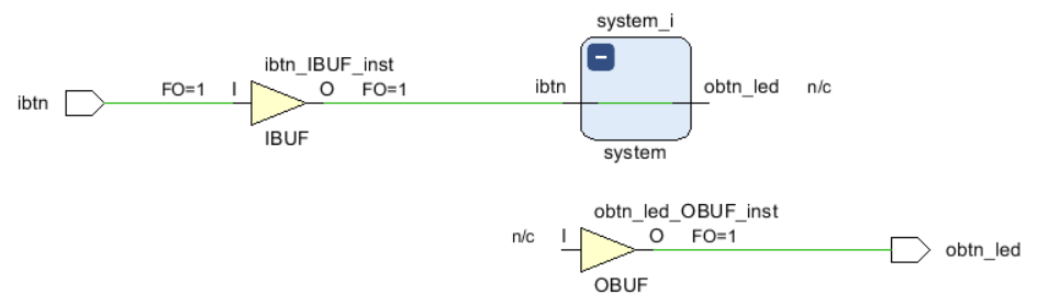
Figure 95 - Schematic after an open circuit
Also note the Scratch Pad tab, the contents of which have changed.
Now add an inverter to the circuit. Click the Create Cell line in the Edit section, enter the name of the invertor component, find the INV template and click OK (Fig. 96)
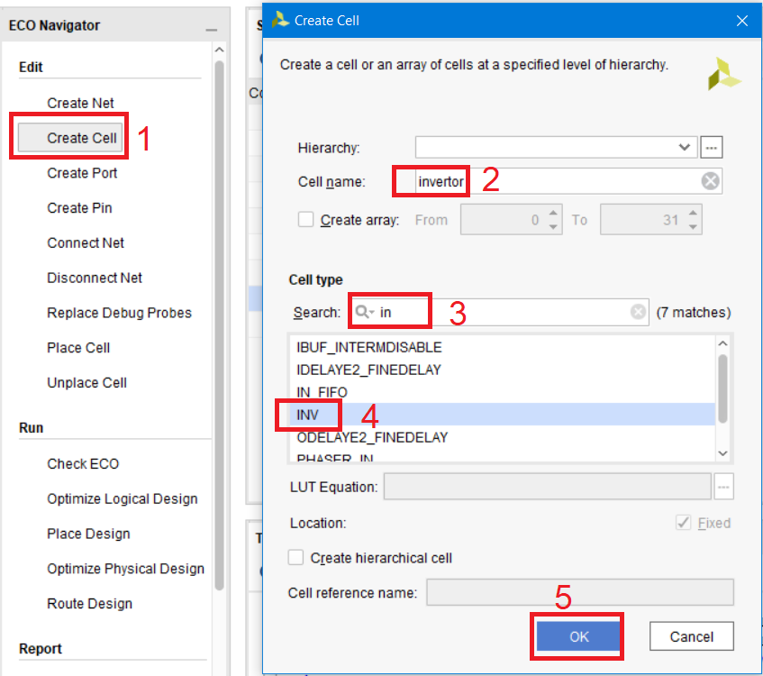
Figure 96 - Creating an inverter
The INV component will be added to the field (Fig. 97)
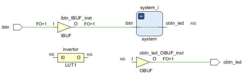
Figure 97 - Created inverter in the circuit field
As you can see, the inverter is implemented on the LUT. To see the logical function that the LUT implements and to change it if necessary, you can right-click on the component to select the Cell Properties properties, in the Truth Table tab, click Edit LUT Equation ... (Fig. 98).
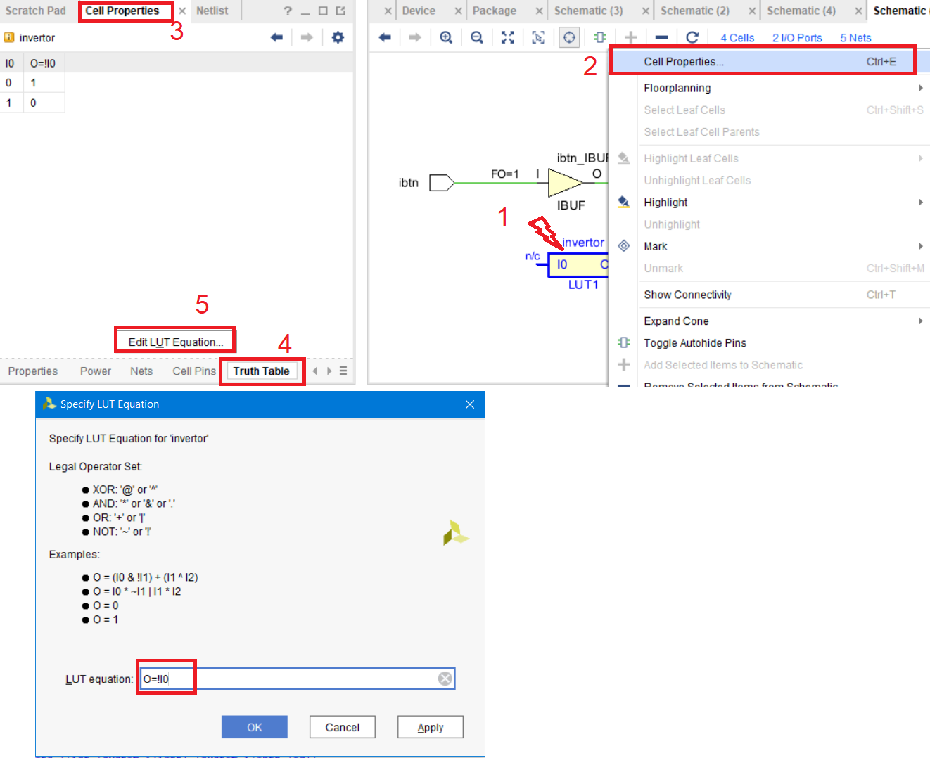
Figure 98 - Property and table of the logical function LUT
Connect the pins. Select either the schematic or the Scratch Pad tab of the I0 pins of the invertor component and the obtn_led system_i component.
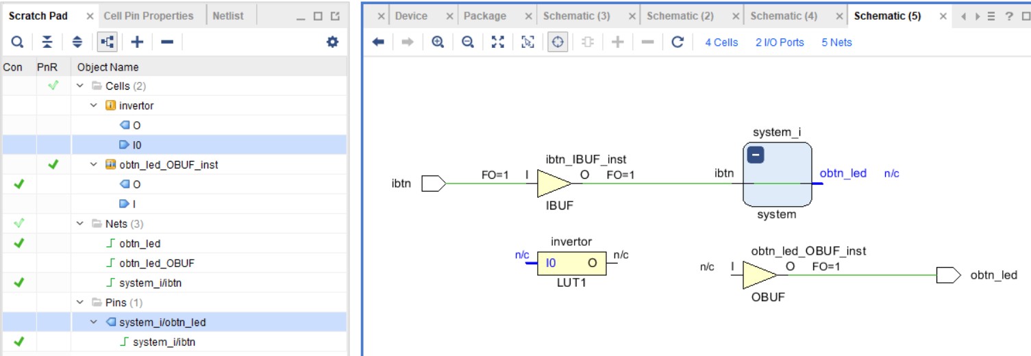
Figure 99 - Selecting connectable pins
Now create a chain between them. To do this, in the Edit section, click the Create Net button. In the dialog box, enter the name of the created circuit btn_led, check the box for automatically connecting two ports and click OK (Fig. 100)
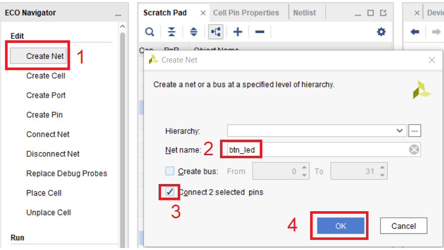
Figure 100 - Parameters of the created circuit
After that, two pins will be automatically connected. Click Regenerate Layout (Figure 101)

Figure 101 - Created chain
Repeat the steps for the two remaining pins and connect pin O of the invertor component to pin I of the component obtn_led_OBUF_inst. We will name the chain differently, since there cannot be two chains with the same names in the design at the same hierarchy level. Call the chain btn_led_o. The connection result is shown in fig. 102
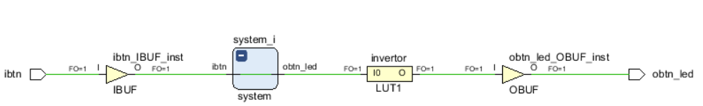
Figure 102 - Schematic with the created inverter
Now we save our DCP and check for errors before starting the placement and tracing of new components (Fig. 103).
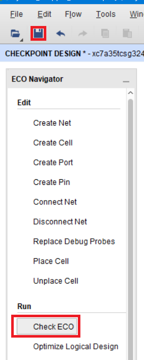
Figure 103 - Checking ECO for errors
Due to the fact that we did not perform placement and tracing, a number of errors will appear that speak of this.
Now let's try to generate a bit of the firmware file, and see if it turned out to make the changes correctly. To do this, you must sequentially follow the steps from the Run section, not everything is clear and without any options. Everything remains by default (Fig. 104).
Click Place Design and without entering any options, click OK. After waiting for the completion of operations, click Route Design and select Incremental Route in the window that appears, click OK.
After that, we generate a bit file by clicking on Generate Bitstream. Verify that the edited_dcp folder is specified in the file path field. After that, open the Hardware Manager for flashing our FPGA.
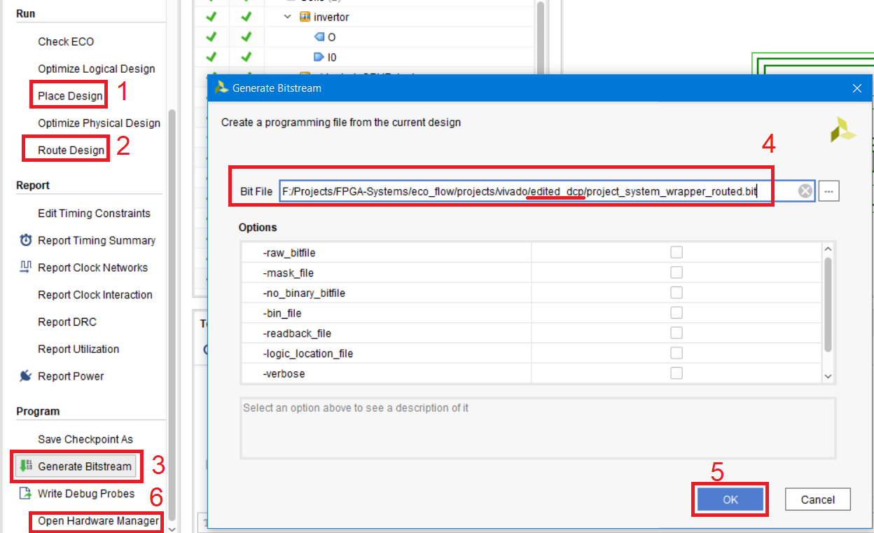
Figure 104 - The sequence of steps to obtain the .bit firmware file
When opening, please note that a new instance of Vivado will open. But it didn’t open for me, so I just open a new instance of Vivado and launch Hardware Manager (Fig. 105). In this case, be careful when choosing the .bit firmware file and the net file for ILA .ltx
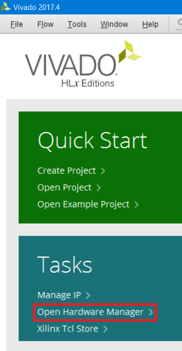
Figure 105 - Opening Hardware Manager from the initial Vivado window
Perform the sequence of actions according to Fig. 67-69 and program the FPGA. Please note that we will be flashing the file located in the edited_dcp folder (Fig. 106).
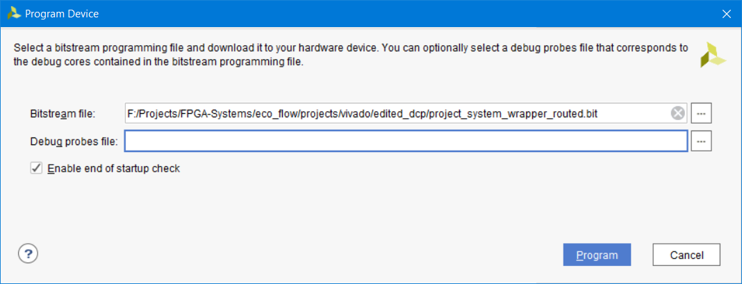
Figure 106 - FPGA firmware file with modified netlist
If everything was done correctly, then the LD0 LED should light up, and go off when the BTN0 button is pressed.
6.2. Change component properties / parameters
In ECO mode, it is also possible to change the contents of components and change their parameters. Now we will try to change the contents of the block memory of the brom_reader module, which imitates, for example, filter coefficients. Let's find our BROM and look at its INIT property, which is responsible for initial initialization.
Go to the Netlist tab and find the block memory in the brom_reader module (Fig. 107).
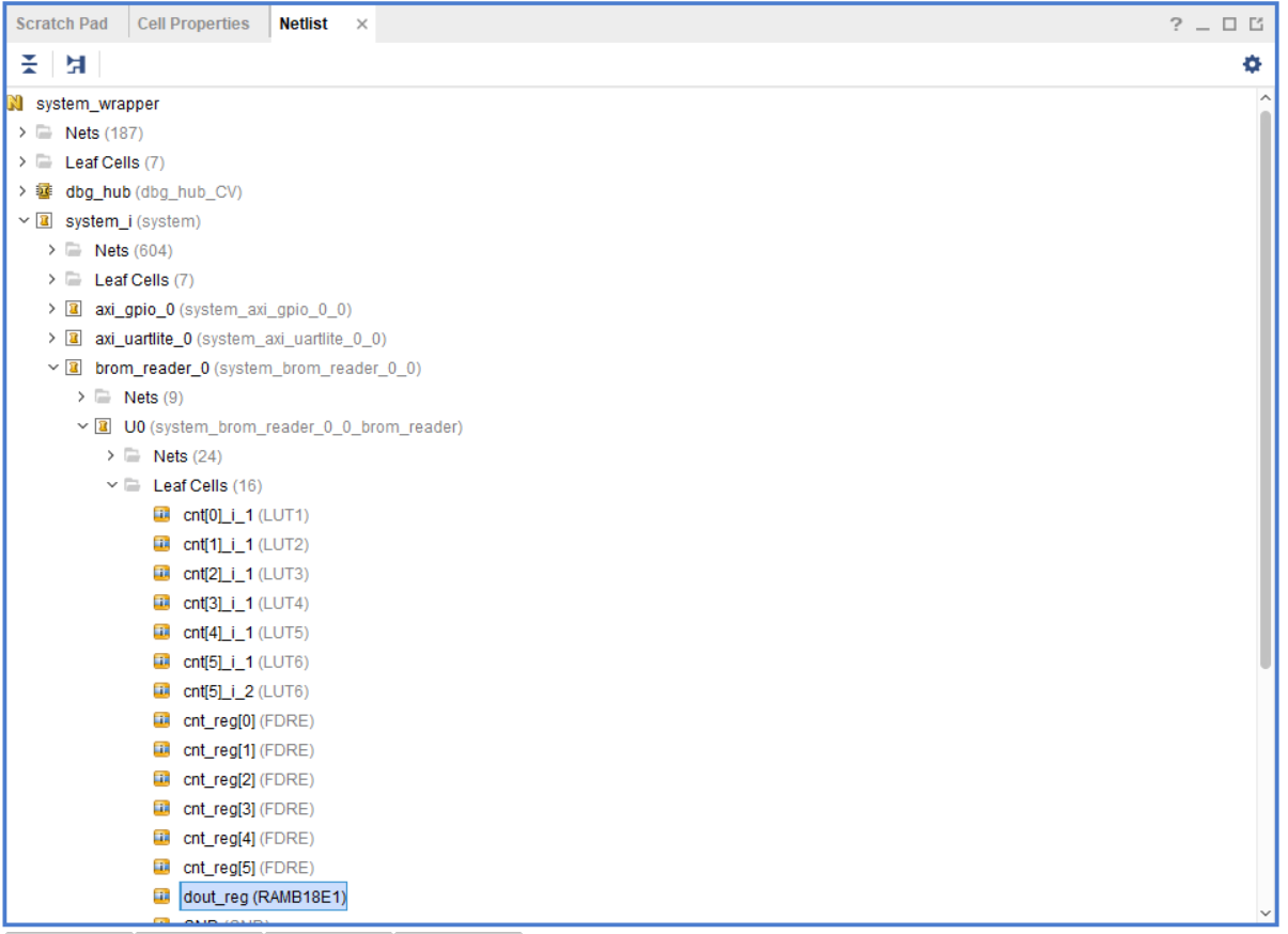
Figure 107 - Location of block memory of brom_reader module in netlist
By right-clicking on this component, we can view its properties by selecting Cell Properties (Fig. 108). Then go to the Properties tab and scroll to the INIT properties.
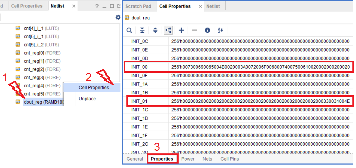
Figure 108 - INIT properties of the selected block memory
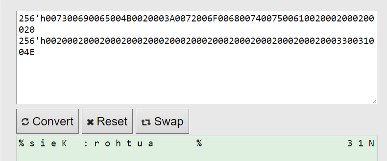
As you can see, the initialization values of the block memory are stored in the INIT properties. Among the many properties, we are only interested in INIT_00 and INIT_01. If we copy the contents of these two properties, the HEX to ASCII converter [15], we get the inscription, which we saw in Fig. 77, but written in the reverse order (Fig. 109) Figure 109 - The contents of the INIT properties in ASCII format
You can change the component property by clicking on the pencil icon and entering new values or using the Tcl console and set_ptoperty command.
Replace the property values according to Fig. 110 and save the result:
INIT_00: 256'h0061006700700066002E00770077007700200020002000200020002000200020
INIT_01: 256'h0020002000200020002000750072002E0073006D00650074007300790073002D
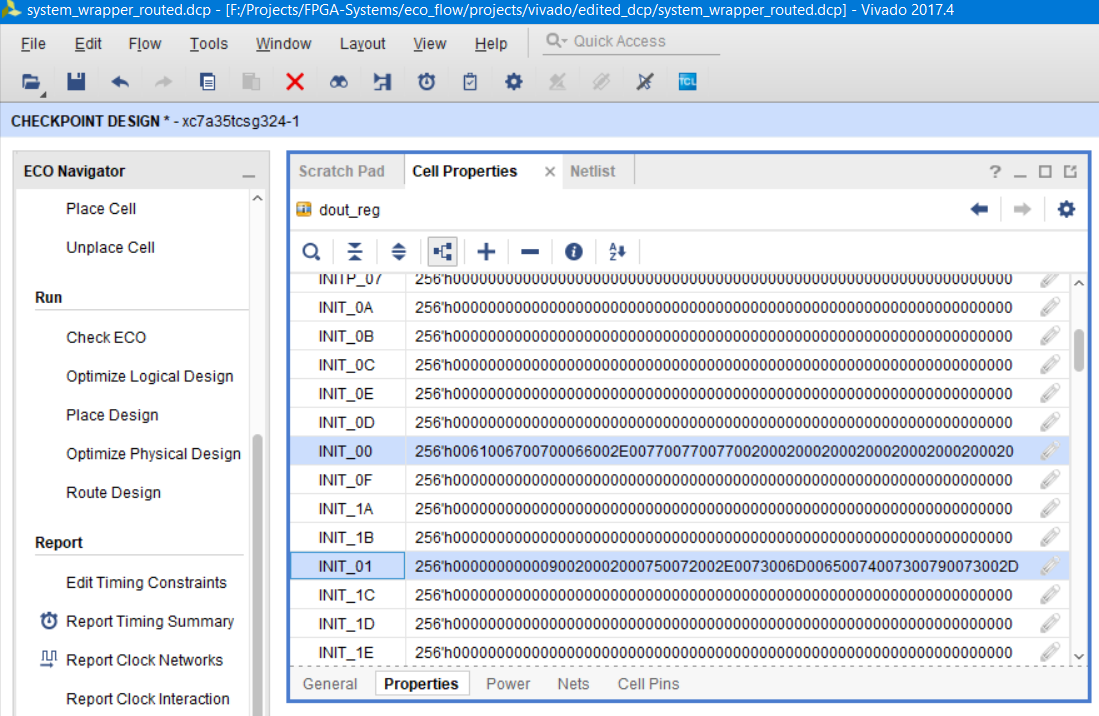
Figure 110 - Modified contents of INIT properties in ASCII format
Since we did not add new components to the netlist or reconnect the circuits, there is no need to perform placement and tracing . Just click Generate Bitstream and wait for the operation to complete. Just in case, generate a .ltx file, which we pick up during debugging (Fig. 111).
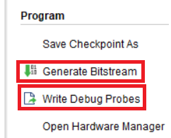
Figure 111 - Generating a bitstream and circuit file for debugging
Go to the Hardware manager and program the FPGA with the newly generated .bit file and the created .ltx probe list (Fig. 112). Please note that the files are taken from the edit_dcp folder.

Figure 112 - Modified netlist and netlist firmware files
Follow the sequence of actions described in fig. 73-75 (open hw_ila_2, convert the type of displayed values to ASCII and view the displayed label). If everything turned out correctly, then the inscription fig. 113.

Figure 113 - Modified contents of block memory
As you can see, if you need to change the contents or parameters of components not only of block memory, but in principle of any components that do not require interferences in placement and tracing, then this is done very quickly and quite simply. However, you should be careful when you change the parameters that are responsible for the operating frequency, for example, when you make changes to the MMCM or PLL settings of your project. In this case, before creating the firmware file, make sure that the project timings converge and the corresponding reports do not give errors (Report Timing Summary, etc.).
6.3. Connecting Other Circuits to Probes and ILA
Perhaps the most useful use case for ECO is to replace, in an already implemented project, circuits connected to probes. The only limitation here is that all virtual probes should be connected, none should be “hanging in the air”. This limitation is usually not significant, since unused probes can always be simply connected to gnd or vcc.
Let's try to switch the probe that observed the output of the block memory to the counter value generating an address for it.
As we know from the description of the ECO interface, it has a tool that allows you to reconnect probes; and use it.
Note: despite the availability of a special editing tool for probes and connected circuits, you can perform these actions “completely manually”, similar to what we did when adding a component: disconnect some circuits and connect others. However, there are some nuances: for reasons that are not completely clear, sometimes the circuit cannot be disconnected from the pin, clicking on Disconnect Net is not performed. In this case, you can either remove the “DONT_TOUCH” property from the chain with your hands or through scripts or cancel its trace (execute “unrote”) - then Disconnect Net will be executed. When working as a master, such problems are not observed.
Working with a wizard requires us to know the name of the circuits that we are going to connect. Let's try to find the chains responsible for setting the address for block memory in the brom_reader module. This can be done through a schematic representation or through the netlist itself. Since the module is small, we simply look through the name through a netlist (Fig. 114). The required circuit is called cnt, it is a bus with a width of 5.
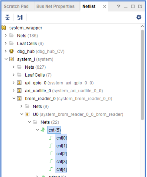
Figure 114 - The block memory address chain in netlist
Select Replace Debug Probes mode. Since our counter only counts to 31, only 5 lines are required, so select the first five lines in ila_1, then right-click and select Edit Probes (Fig. 115). You can choose any ila, but they are quite bulky. For guidance, selected simpler.
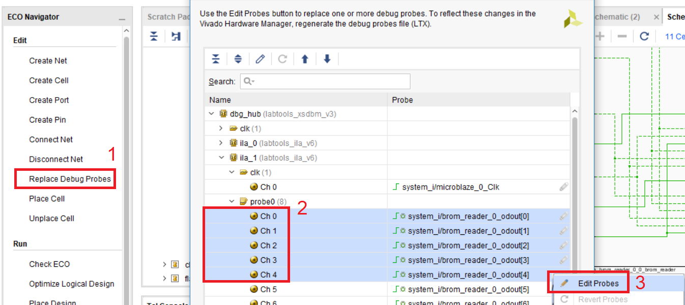
Figure 115 - Selection of replaceable probes
We search the net list by entering the name of the net we are looking for * cnt [*]. Scrolling down we find them, and press the add to probes button. Please note that we are replacing 5 probes at the same time, so 5 circuits must be selected. Replacing the search type from contains to match is determined by the search rules in tcl and for the current example allows you to display a more accurate result. When using circuit search, it is recommended that you at least understand and know the wildcard characters in Tcl and the rules by which the search is performed.
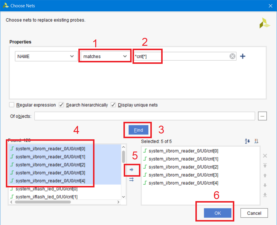
Figure 116 - Search for circuits connected to the probes
We will connect the remaining three chains to "0", in Vivado the chains connected to gnd are called const0. Select the three remaining chains, right-click Edit Probes (Fig. 117).

Figure 117 - understaffing ila_1
We enter the name in the search bar * const0 and add the first chain from the list, clicking the arrow three times, since we must connect three lines (Fig. 118). BE CAREFUL!!! Do not add lines from the Debug Hub hierarchy (dbg_hub), in this case Vivado will give an error only at the very end of the probe setup, and all work will go to the smarck. Select a chain from any IP, for example, uartlite.
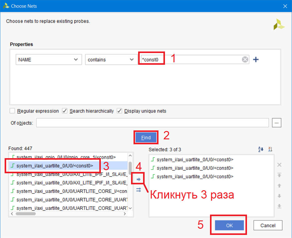
Figure 118 - Adding constant circuits to probes
The formed ila_1 should look like in Fig. 119. Once again, I note that there should be no empty probes. In this case, there will be errors at the DRC stage.

Figure 119 - New chains in ila_1
After clicking on the OK button, a window appears that informs that the DONT_TOUCH attribute will be removed from the circuits previously connected to the ila_1 probes. This is one of the nuances that I described in the note at the beginning of this section. Keep this in mind if you do not use the connection wizard, but do everything manually. We agree with the changes by clicking Unset Property and save the current state of the DCP.
Now we sequentially perform the placement, tracing, bitstream generation and creating a list of circuits (Fig. 120). All together takes about 1 minute on my computer. Fast, isn't it!
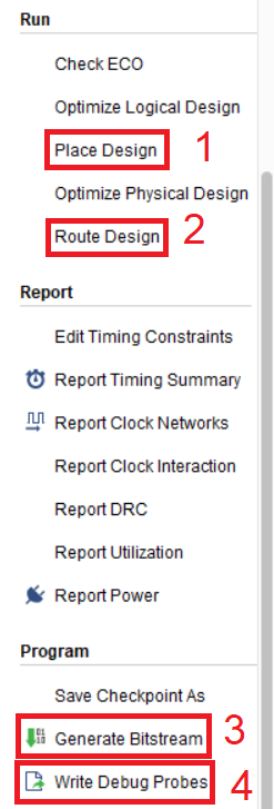
Figure 120 - a sequence of steps to create a circuit list firmware file for debugging
Now open the Hardware Manger and program our crystal, forgetting to connect the correct .bit and .ltx files.
Opening hw_ila_2 we will see 4 signals: the cnt bus and three const0. Change the output of the cnt bus values from hex to unsigned decimal (similar to Fig. 75) and start recording by clicking the blue triangle. If everything is correct, then you will see a change on the cnt bus from 0 to 31 with increment 1 (Fig. 121).
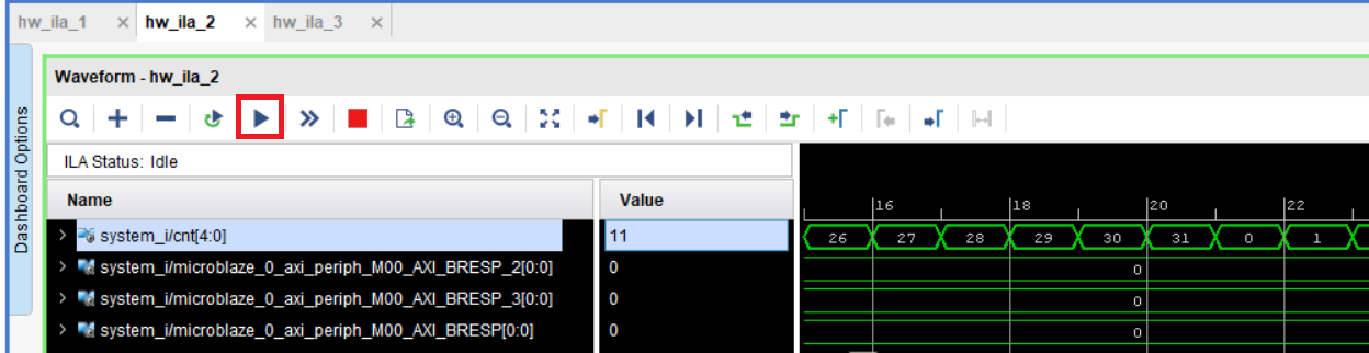
Figure 121 - The value of the cnt bus in the ila_1 probe
As you can see, we were able to disconnect the output circuits of the block memory from the probes and connect new ones.
6.4. Replacing I / O Ports
The last thing left to do is change rx and tx for the uart module and finally see Hello World in the console. It should be noted that when working with ECO there are several ways to achieve the result. I will show one of them.
Tear off the netlist. Before proceeding with the reassignment of the legs, it is worth writing that it will be necessary to remove the entire input circuit to the first object of type cell, after which it will simply be restored again. We will delete the port, circuit and buffer.
First, let's figure out the input circuit.
Select the uart_rtl_0_rxd port, the circuit connected to it and the input buffer. Click unplace cell and then delete (Figure 122). After clicking the delete button, the port will remain, just select it and click delete one more time.
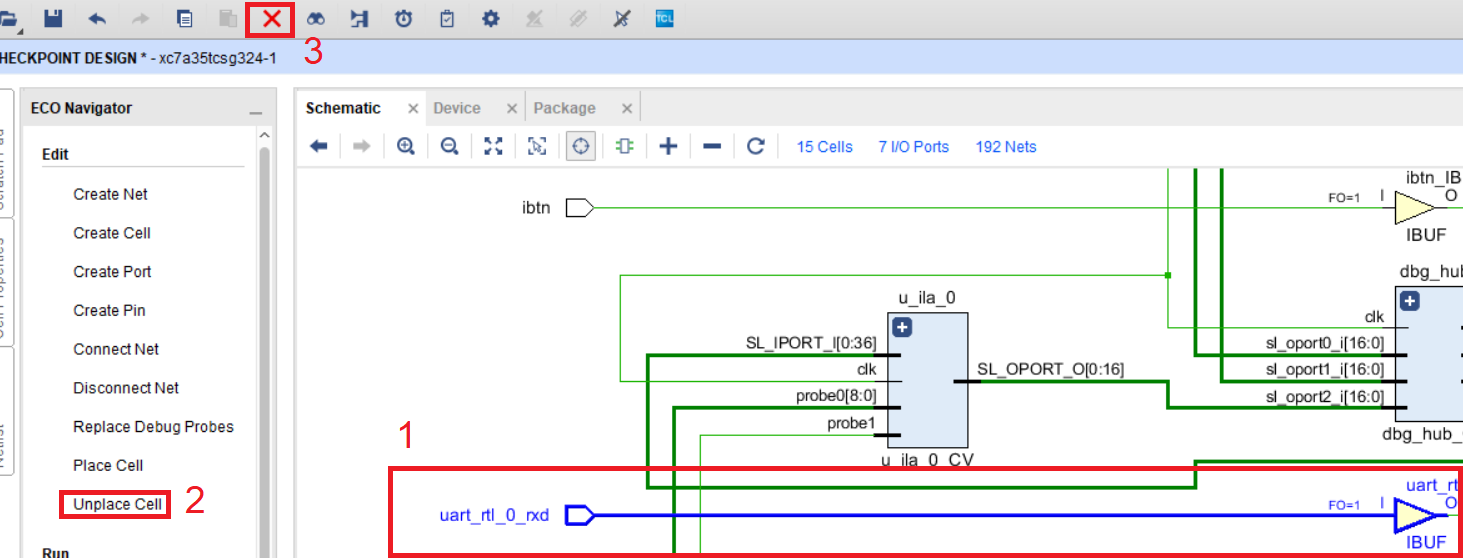
Figure 122 - Input circuit selection and component tracing
Now recover the deleted components. First, add the uart_rx port by clicking on the Create Port button and then setting the settings in accordance with Fig. 123

Figure 123 - Parameters of the created input port
Since the A9 leg is already occupied by our output port, Vivado will display a message asking you to unlink the other port to the A9 leg. We agree with this (Fig. 124)
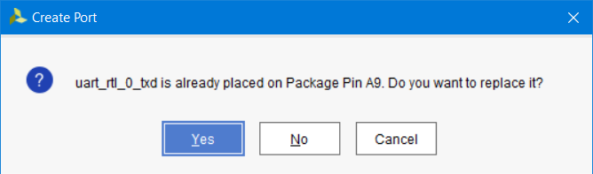
Figure 124 - Information window on an existing connection to the selected leg
Now create an input buffer. Press the Create Cell button, the name of the ibuf_rx cell to be created (Fig. 125)
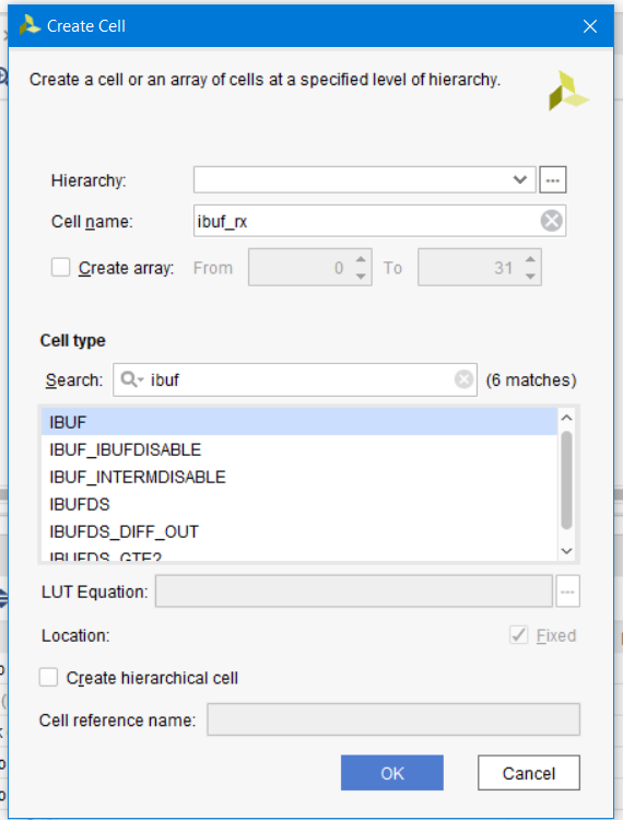
Figure 125 - Creating an input buffer
Now create a chain. This is done in several stages. First, the circuit connects to the port, and then connects to the buffer. Select the uart_rx port and click Create Net. The name of the chain is rx_net.
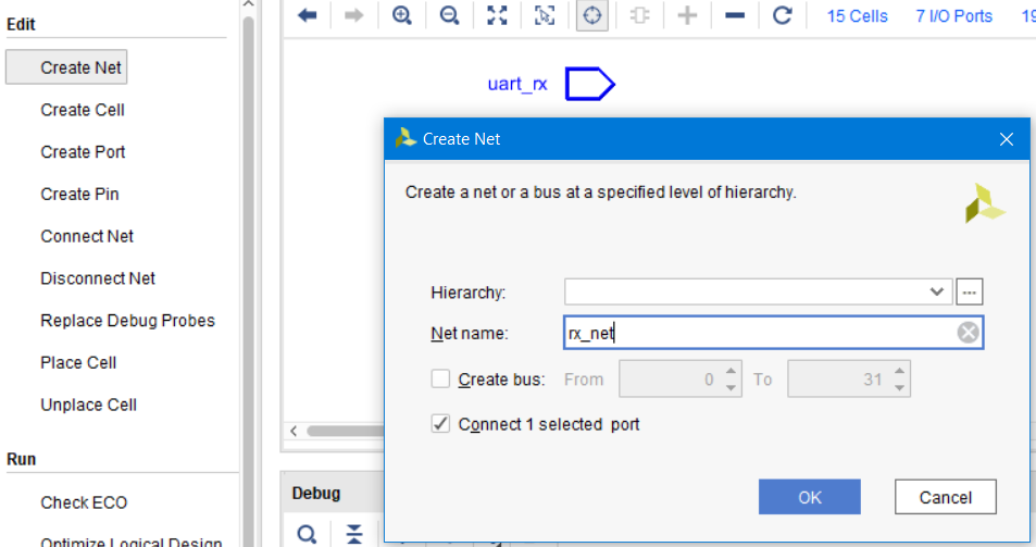
Figure 126 - Creating a chain
Now select the chain and port I of the input buffer and click Connect Net. After that a chain will appear (Fig. 127)
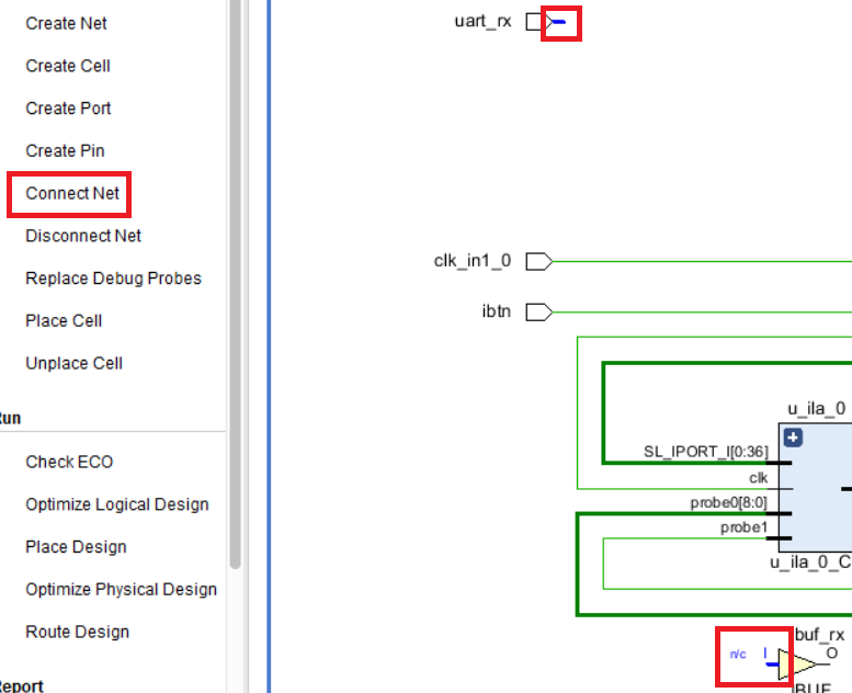
Figure 127 - Connecting the port and input buffer
Now create a chain between the buffer and the system_i module. Select the output pin O of the buffer and the circuit uart_rtl_0_rxd connected to system_i and click Create Net
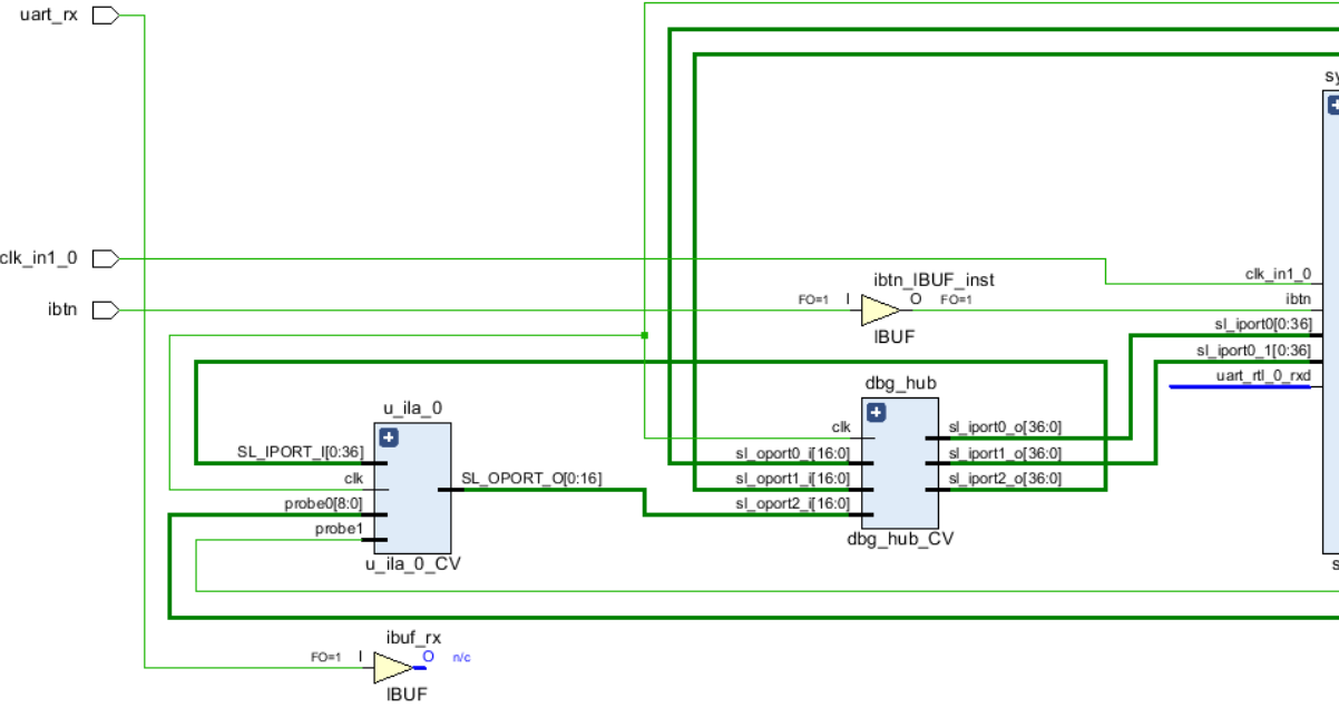
Figure 128 - Buffer and circuit connection
Now we repeat the same sequence of actions for the output port.
Select the output port uart_rtl_0_txd, the circuit connected to it and the output buffer. Click Unplace cell, and then the red cross to remove the components (Fig. 122). After clicking the delete button, the port will remain, just select it and click delete one more time.

Figure 129 - Output circuit selection
Create the uart_tx port by clicking the Create Port button, set the Output direction and set the standard LVCMOS33 (Fig. 130)
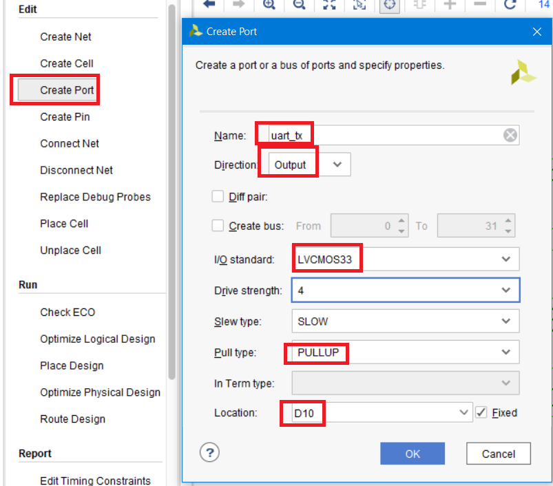
Figure 130 - Setting the output port parameters
Create a tx_net chain that will be connected to the uart_tx port. Select uart_tx and click Create Net

Figure 131 - Creating a tx_net chain
Create the tx_obuf output buffer by clicking Create Cell and choosing the OBUF type (Fig. 132)
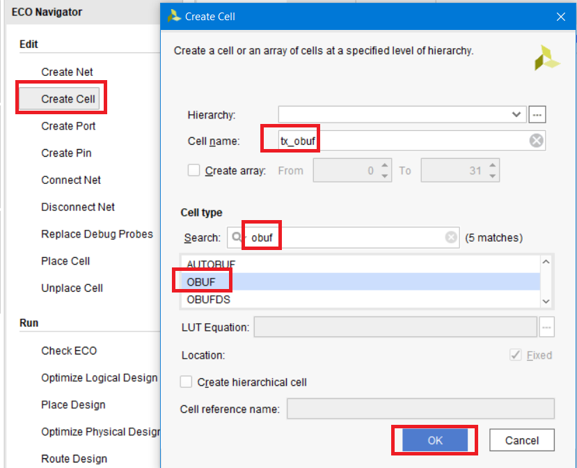
Figure 132 - Creating an output buffer
Select pin O of the output buffer and the circuit connected to the uart_tx port and click Connect Net.

Figure 133 - Buffer and port connection
Now connect the buffer to system_i. Select pin I of the buffer and chain uart_rtl_0_txd (Fig. 134).

Figure 134 - Buffer and circuit connection
We save the project and execute sequential placement and tracing. After this starts the bistrim generation (Fig. 135).

Figure 135 - Sequential steps to obtain a firmware file
Open the Hardware Manager and program the FPGA. Go to the SDK and run the application (see Figure 70). If everything is fine, but in the console you will see the message Hello World: cycle (Fig. 136).

Figure 136 - Hello World messages in the Terminal SDK
7. Comparative analysis
We will conduct a small comparative analysis of different approaches to making changes to the project in terms of the time spent on various operations. This comparison will, of course, be rather arbitrary, because the required time greatly depends on the crystal, on its congestion, on the number of free trace resources, etc. Operations will be performed on changing HDL files, after which the synthesis will be performed anew, and also in the “postsynthesis” netlist, probes will be changed. The results are shown in table 1. It should be noted right away that incremental implementation gives a gain only when working with large crystals, for which obtaining the final result can take ten hours. The time taken to make changes by the developer was not included in the accounting here. However, the fact that
Table 1. Comparative analysis of the time taken to obtain the final firmware file in various modes.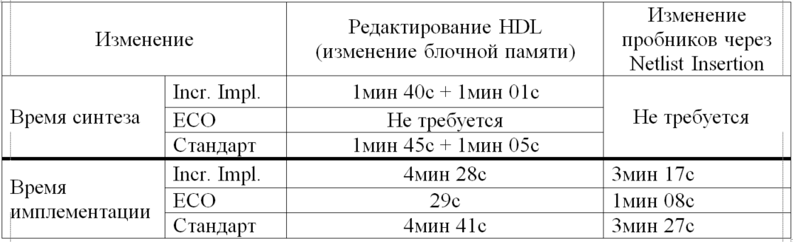
Summarizing the comparative analysis, once again I say that it is very superficial. You perfectly understand that FPGA is a complex system and the time of this or that stage of the design route can change very much. Nevertheless, ECO does not require synthesis, and making small changes to the project is much faster, especially when you want to save the crystal trace and make changes only to the contents of the components.
8. Conclusion
Have I ever applied ECO mode in practice? Yes. The task was, without changing the crystal trace, to change the contents of block memory, in which some values were sewn up, which allowed to protect products from copying. ECO came in handy there; however, for the most part, the work was done using Tcl scripts, not a graphical interface. Nevertheless, ECO mode is really useful when working with large projects - especially if you are an ardent fan of in-circuit debugging with LogicAnalyser (ChipScope) and like to do ILA for a couple of hundred (or even thousands) of probes. Perhaps you will find the work in this mode useful for you if you just try to do something more than described in this guide.
If you found an interesting application for ECO Flow, or just decided to try using it in your project, leave a short comment: it will be interesting to find out why ECO Flow was useful for you at Vivado.
Do not forget to do your homework. Good luck
9. Homework
- Using the corrected netlist, modify the LUT logic function that implements the inverter so that it does not invert the input signal.
- Try running various optimizations with various options in ECO mode. Use the guide with Tcl commands Vivado [9] for help.
- View the transactions on the AXI-lIte bus that go to the GPIO module. In ECO mode, replace the circuits that are connected to ila_1 from the uartlite module with the circuits from the gpio module.
- * Try changing the frequency that the MMCM produces, the current value is 100MHz. Make it 50 MHz. If everything is done correctly, then the LED should flash twice as slow. Do not forget to view the timings report, since you have changed the module that controls the frequency of the entire project.
- * Try to create a Tcl command or script that would automatically perform the necessary sequence of actions when changing netlist in ECO mode. The script should save the changes, run the placement, trace, generate the firmware file, etc.
- ** Write a script that would allow changing the contents of block memory in the brom_reader block, writing down any 32 ASCII characters entered as arguments of the developed procedure / script
Bibliographic list
1. Vivado on the Xilinx website
2. Description of the Arty Board on the Digilent website
3. UG904 Vivado Design Suite User Guide: Implementation
4. UG908 Vivado Design Suite User Guide Programming and Debugging
5. UG986 Vivado Design Suite Tutorial: Implementation
6. Wiki : ECO
7 . UG949 UltraFast Design Methodology Guide Review
8. UG892 Vivado Design Suite the User Guide Review Design Flows Overview Profile
9. UG835 Vivado Design Suite the Tcl the Command the Reference Guide Review
10. UG894 Solution: Using the Tcl the Scripting
11.UG901 Vivado Design Suite User Guide Synthesis
12. Arty Reference Manual
13. UG908 Programming and Debugging
14. UG1037 Vivado Design Suite AXI Reference Guide
15. Hex-to-ASCII
16. Manual: Developing a processor system based on the MicroBlaze software processor in Xilinx Vivado IDE / HLx
Appendix A. Listing flash_led module
library IEEE;
use IEEE.STD_LOGIC_1164.ALL;
entity flash_led isPort ( iclk : inSTD_LOGIC;
           oled : outSTD_LOGIC);
end flash_led;
architecture rtl of flash_led issignal cnt : naturalrange0to100_000_001 := 0;
    signal led : std_logic := '0';
beginprocess(iclk)
    beginif rising_edge(iclk) thenif cnt = 100_000_000then
                cnt <= 0;
            else
                cnt <= cnt + 1;
            endif;
            if cnt < 50_000_000then
                led <= '0';
            else
                led <= '1';
            endif;
        endif;
    endprocess;
    oled <= led;
end rtl;
Appendix B. Listing of brom_reader module
library IEEE;
use IEEE.STD_LOGIC_1164.ALL;
use IEEE.NUMERIC_STD.ALL;
entity brom_reader isPort (
        iclk : inSTD_LOGIC;
        odout : outstd_logic_vector(7downto0)
        );
end brom_reader;
architecture rtl of brom_reader isalias slv isstd_logic_vector;
    type rom_type isarray (0to31) ofnatural;
    signal rom : rom_type := (
		32 ,  32,  32,  32,  97, 117, 116, 104,
		111, 114,  58,  32,  75, 101, 105, 115,
		78 ,  49,  51,  32,  32,  32,  32,  32,
		32 ,  32,  32,  32,  32,  32,  32,  32
	);
    signal cnt : naturalrange0to rom'length-1 := 0;
    signal dout: slv(odout'range) := (others => '0');
    attribute RAM_STYLE : string;
    attribute RAM_STYLE of rom : signalis"BLOCK";
beginprocess(iclk)
    beginif rising_edge(iclk) then
           dout <= slv(to_unsigned(rom(cnt), dout'length));
           if cnt = (rom'length - 1) then
            cnt <= 0;
           else
            cnt <= cnt + 1;
           endif;
        endif;
    endprocess;
    odout <= dout;
end rtl;
Appendix B. Listing the helloworld program
#include"platform.h"#include"xil_printf.h"#include"xparameters.h"#include"xgpio.h"
XGpio Gpio; /* The Instance of the GPIO Driver */#define DELAY 10000000intmain(){
    init_platform();
    int Status;
    volatileint Delay;
    int k = 0;
    /* Initialize the GPIO driver */
    Status = XGpio_Initialize(&Gpio, XPAR_GPIO_0_BASEADDR);
    if (Status != XST_SUCCESS) {
    	xil_printf("Gpio Initialization Failed\r\n");
    	return XST_FAILURE;
    }
    /* Loop forever blinking the LED */while (1) {
		/* Set the LED to High */
		XGpio_DiscreteWrite(&Gpio, 1, 1);
		xil_printf("Hello World: cycle %d\n\r", k);
		k++;
		/* Wait a small amount of time so the LED is visible */for (Delay = 0; Delay < DELAY; Delay++){};
		/* Clear the LED bit */
		XGpio_DiscreteWrite(&Gpio, 1, 0);
		/* Wait a small amount of time so the LED is visible */for (Delay = 0; Delay < DELAY; Delay++){};
    }
    cleanup_platform();
    return0;
}
PS: Many thanks to users of intekus Des333 , ishevchuk , roman-yanalov who not only read this 91 page manual (this is how much it takes in Word), but also completed it and made the necessary editorial changes.