Using custom 25 Series DataFlash instead of expensive Altera FPGAs without additional hardware
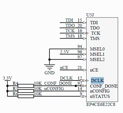
From any description of popular FPGAs it is known that special microcircuits are used to store their configurations - configurators. In the comments, they corrected me that FPGA is slowly gaining popularity, where it is not required, but so far many people are doing development work on the classics, where a configurator is needed, and this should be taken into account. For example, Altera Cyclone uses EPCS chips. Below is a diagram from a typical prototype motherboard with a crystal from the Cyclone IV family. On it we see the EPCS16 configurator. Everything would be fine, but traditionally these configurators are quite expensive, so I would like to use something cheaper.
Details in the long text below. If it’s very interesting, but too lazy to read so many letters, you can simplify the task by watching a detailed 20-minute video.
So, back to our problem.

If you turn in your hands the very breadboard with a crystal of the Cyclone IV family, then we will see a very amazing thing.
Here it is, PLISina, and here is the configuration ROM:
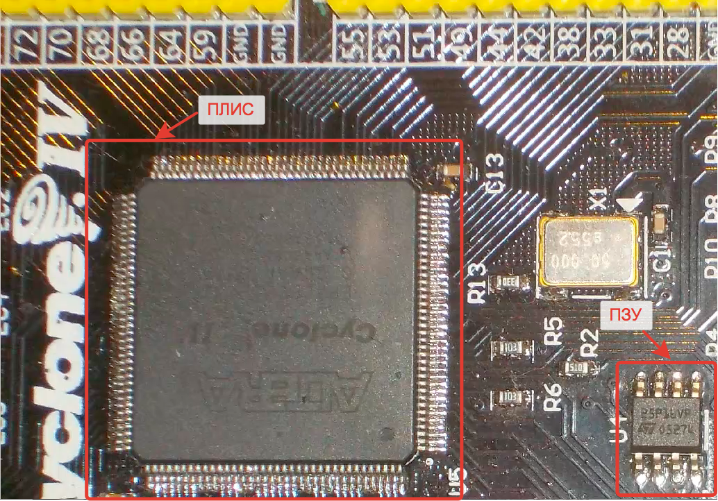
Oddly enough, this is not EPCS, but the usual 25th flash drive. Such flash drives are cheap and sold quite a lot from anyone.
But as they say, not all yogurts are equally useful. In particular, our customers joyfully bought such flash drives, soldered on a board and got a global problem. We go into the programmer, load the file prepared for the firmware, start flashing it and get an error:
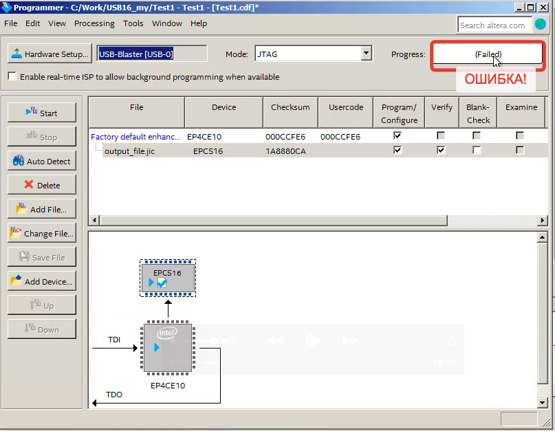
Here is the error message:
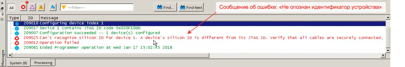
Error (209025): Can't recognize silicon ID for device 1. A device's silicon ID is different from its JTAG ID. Verify that all cables are securely connected, select a different device, or check the power on the target system. Make sure the device pins are connected and configured correctly.
The device identifier is not recognized. That is, the flash drive has an unknown identifier in terms of a quartus. Specifically, 25P32 crystals were purchased from our customers, which are generally not supported in principle, but there may be a more mundane situation in life. In particular, the ST flash drive is soldered in the photo above, and it is defined as MICRON. Chinese sellers and not so can mark, and when the batch is purchased and does not work - what can be done?
I climbed into the forums. All the Russian-speaking ones that were able to be inspected were full of discussions, which suppliers and what should be taken so as not to run into a similar problem. But in our case, no one wanted to buy a new batch. In English sources, only one article was found with a solution, but in the modern Quartus Prime environment, this solution will not work “head-on”. Therefore, we undertook to document this problem for the modern environment, in Russian and in video format.
So, how is ROM generally programmed?
A special configuration is poured into the FPGA, which makes it possible to tap through the JTAG to the flash drive. And then, using this configuration, we fill in the data. It turns out that you can make a similar configuration, which will give us access to the USB flash drive and allow us to flash it regardless of the ID, without having to write a single line of our own code, and the utilities will all be used from Quartus Prime (or Qiartus II, who uses old versions of the development environment).
That is, we have to take 3 steps:
Let’s do it. Let's start by developing our own “firmware” (it’s the same configuration) without writing a single line of our code.
We go to Quartus:
We create a new project:
Let's
name it, say, flasher: This name should be remembered - we still need it.
We create an empty project, my family is Cyclone IV E, the crystal used in the project is like this:
So. Finish creating the project, click Finish. The project is created. As already mentioned, we do not write a single line of our code. But you still need to get the environment to do something. To do this, go to Tools - Platform Designer.
Here it booted. Specifically, I have 60 Hz quartz in this board, so I will correct the frequency settings:
What I do now, we do once for the platform. That is, if some kind of board is made, then this bootloader will work for it for any project.
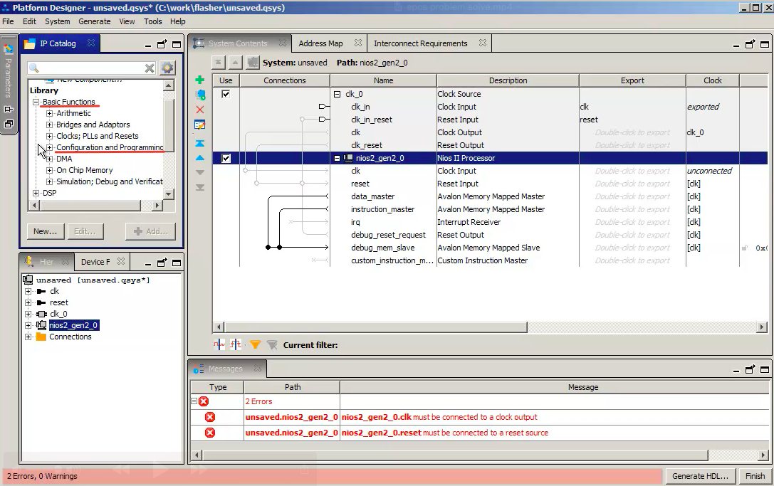
I prepared the quartz - now we put the processor. In the library on the left we find "Processors and Peripherals", "Embedded Processors" and then - Nios II Processor:
Select it and click "Add".
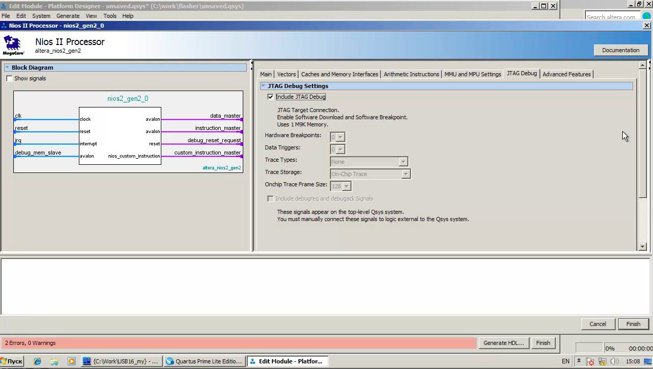
In the window that opens, in the properties, select Nios II / e, because it is absolutely free and it does not need any license.
Errors tell us that the vectors are not configured. We are not going to program anything for this processor. Therefore, we simply direct the vectors to the first place from the list:
It is very important for us that the JTAG module works for the processor:
After our manipulations, the errors are gone.
With the processor over. Click Finish and move on.
Now we go to the main functions. There are configurators here: We
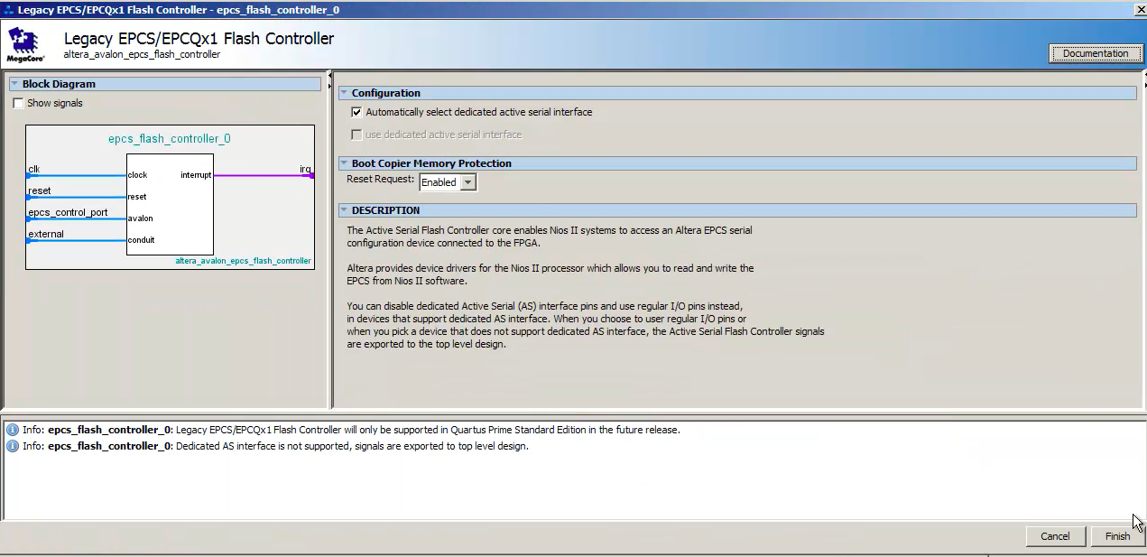
open the list of configurators - near the end we find EPCS - our configurators: We
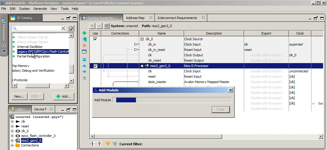
leave everything by default:
Now we begin to connect them. We pass the clock signals to both modules, we pass the reset signal to both modules. The reset signal coming out of the JTAG hardware - debug_reset_request - we also pass to both modules. Next, we skip data_master to both modules. Instruction_master is passed only to the debugger. And we also skip the interrupt request:
Next we go to the external legs - external. We export them, for which we double-click in the Double-click to export field:

For simplicity, I will call epcs so that the length is less:

Now, with the usual hand movement, we assign the base addresses:
And we assign interrupts: The
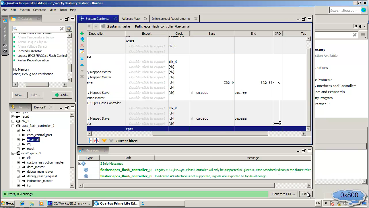
automatically assigned address for our flash controller is 0 × 800 - we should remember:
It will come in handy for us. And everything else, in principle, has done and will work.
Now it is very important, since we are not going to write a single line of our code so that the name of the processor system matches the name of the project. The project we had was flasher.
We save the system, call flasher:
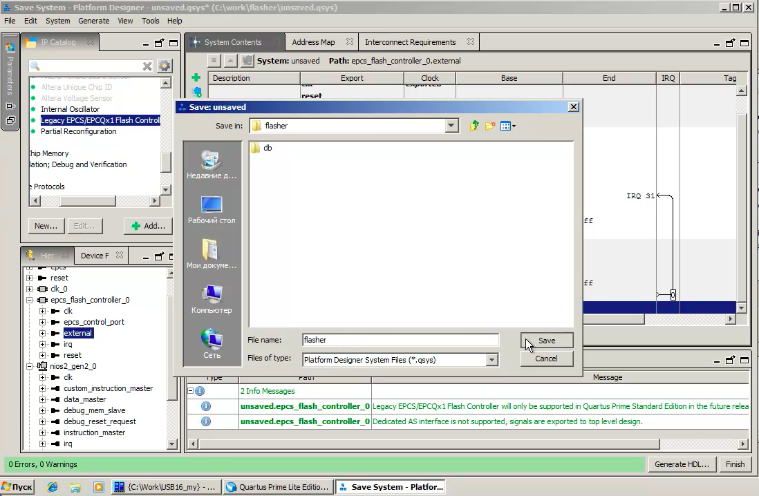
It is then that the top module will have this particular processor, and therefore we will not have to do anything.
Our next step: We
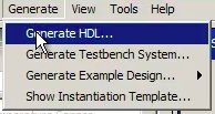
leave everything by default, because we just use what is ready:
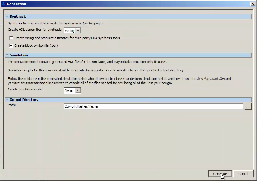
Finish:
There was a message that we need to remember to add the file to the project:
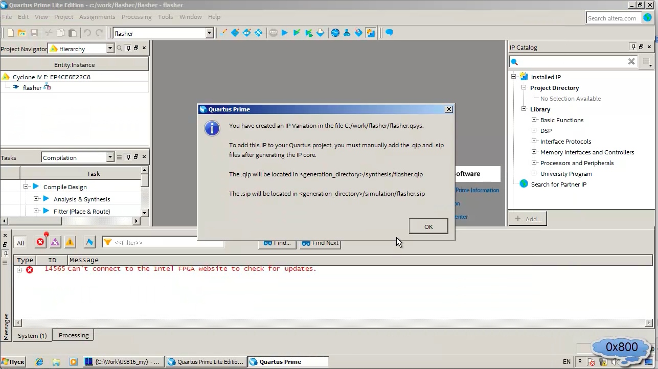
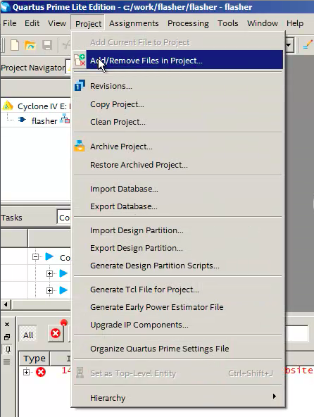
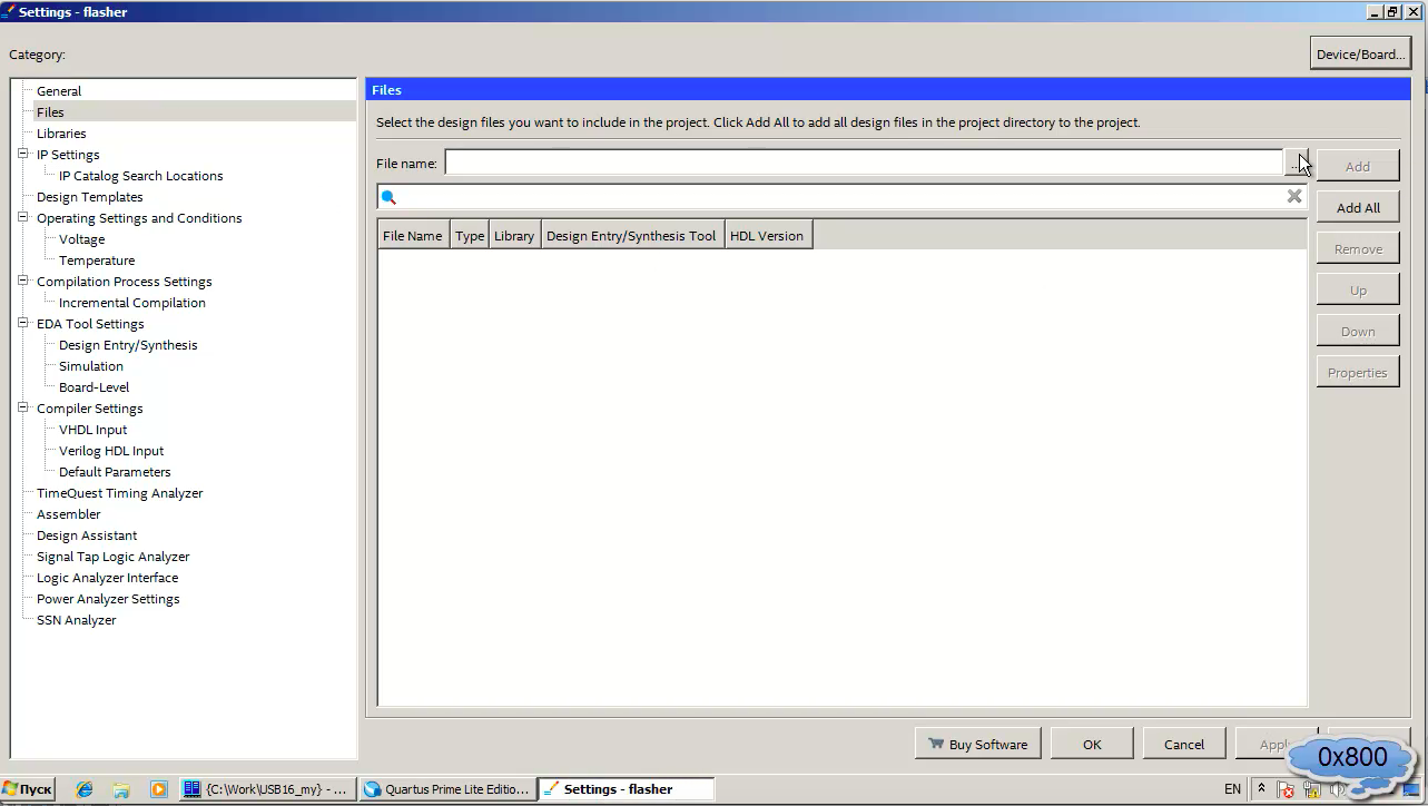
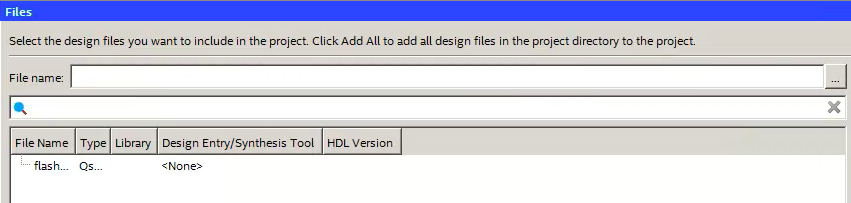
Let's add. Go to Project - Add / Remove Files in Project:
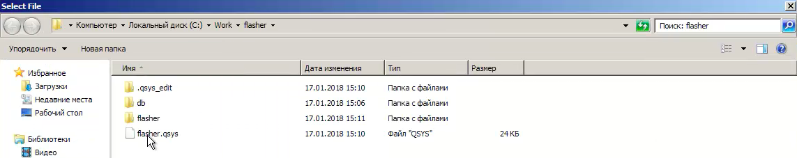
Find our file on the computer.
Here it is, our flasher file with the qsys extension.
Added it:
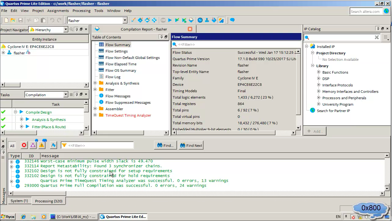
Now we are doing a rough compilation:

It completed successfully.
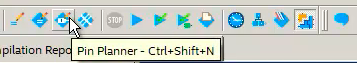
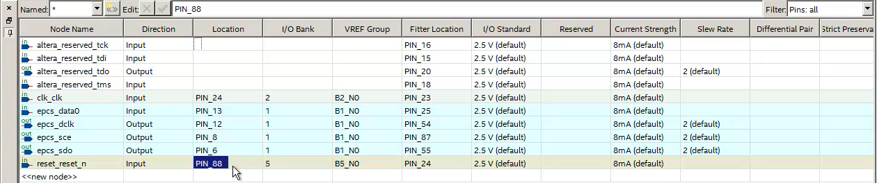
Now that she has passed, we can set conclusions. We go to the Pin Planner:
we don’t need to assign JTAG legs - we assign the legs of a flash drive.
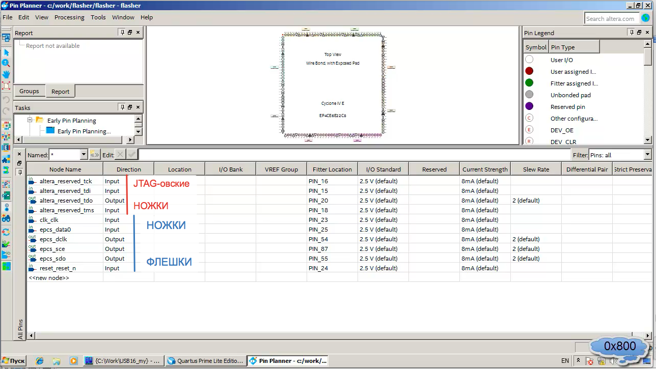
For each chip, for each case they are different. In principle, you can look at the documentation on the chip or on your board. For example, here we have the twelfth leg of DCLK:
I have already prepared the list - just drive it.
So, epcs_data0, LOCATION: PIN13, epcs_dclk - PIN12, epcs_sce - PIN8, epcs_sdo - PIN6. And specifically on the board of our customers, the clock frequency is PIN24, reset_n - PIN88.
The legs are appointed. We start compilation. Errors are issued:
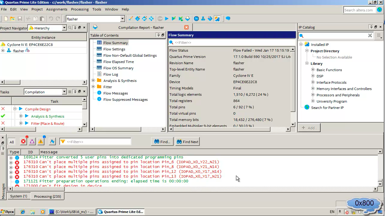
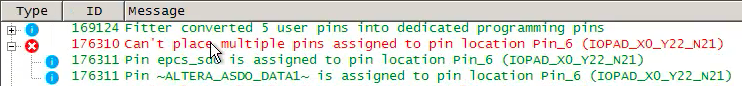
All because I pretended to forget to make a very important setting. We have now connected the USB flash drive to the service lines. And, at the end of the configuration, some of these lines are not available at all, and some are used for official purposes. Therefore, we were given messages that we have a conflict:
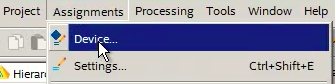
To resolve this, go to Assignments - Device:
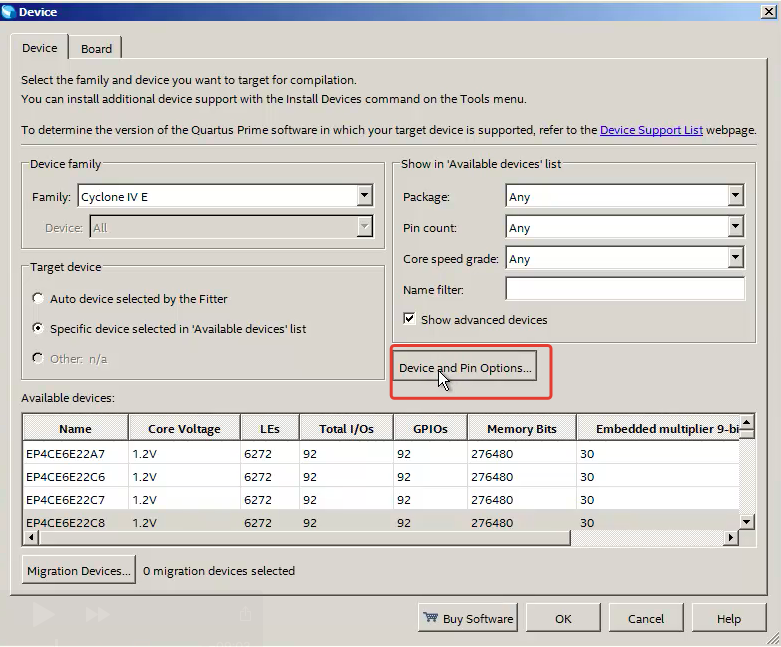
Device and Pin Options:
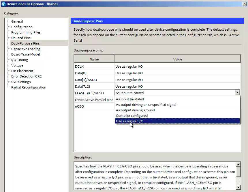
Here we select Dual-Purpose Pins. And at the end of programming, we ask you to make all these lines the usual I / O lines:
Click OK, start the compiler. And it all worked out.
So, the first step is completed. We got a configuration through which we can tap to the flash drive.
Now our task is to create a file with which the system will recognize our USB flash drive.
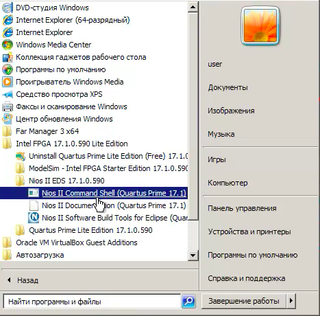
We go to all programs, Intel FPGA (for older versions it will be Altera), Nios II Command Shell.
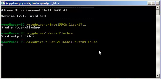
Here we go to the directory where we just collected everything. At the same time, do not forget that the slashes here should not be reverse, but straight, and that the resulting flasher.sof file lies in the output_files directory:
Now we begin to cast magic spells. So, we need to inject the newly formed configuration. To do this, we write:
nios2-configure-sof flasher.sof
and press Enter:
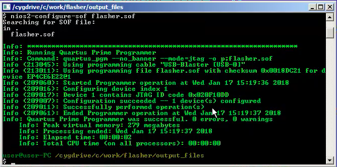
The file is uploaded - now we have access to the flash drive. In order to determine everything regarding access to the flash drive, we need to run the following program:
nios2-flash-programmer --epcs --base = 0x800 - debug.
where 0x800 is the same address that was automatically assigned to the epcs block and which should not be forgotten.

Press Enter:
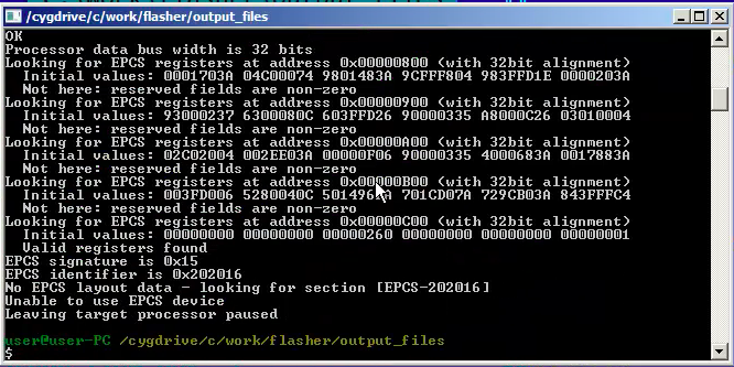
What did he tell us? He tried to inspect the area that we named. And at offset 0 at 800 I did not find anything. At address c00 he found what we needed:
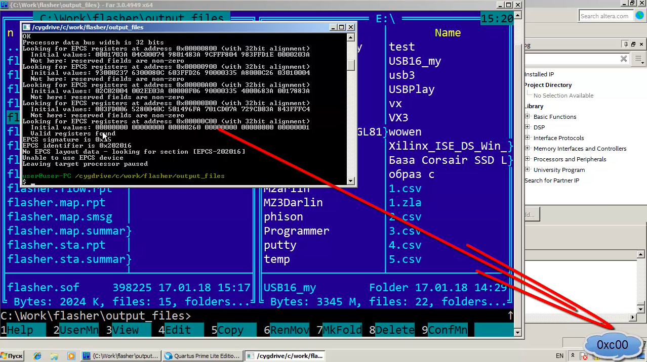
Now we remember not just the base address 800, but the specific address c00 - in the future we will work with it.
He found a flash drive, its identifier is 202016, but said that it has no idea what to do with it, because it does not know it.
Here is the documentation for our flash drive:
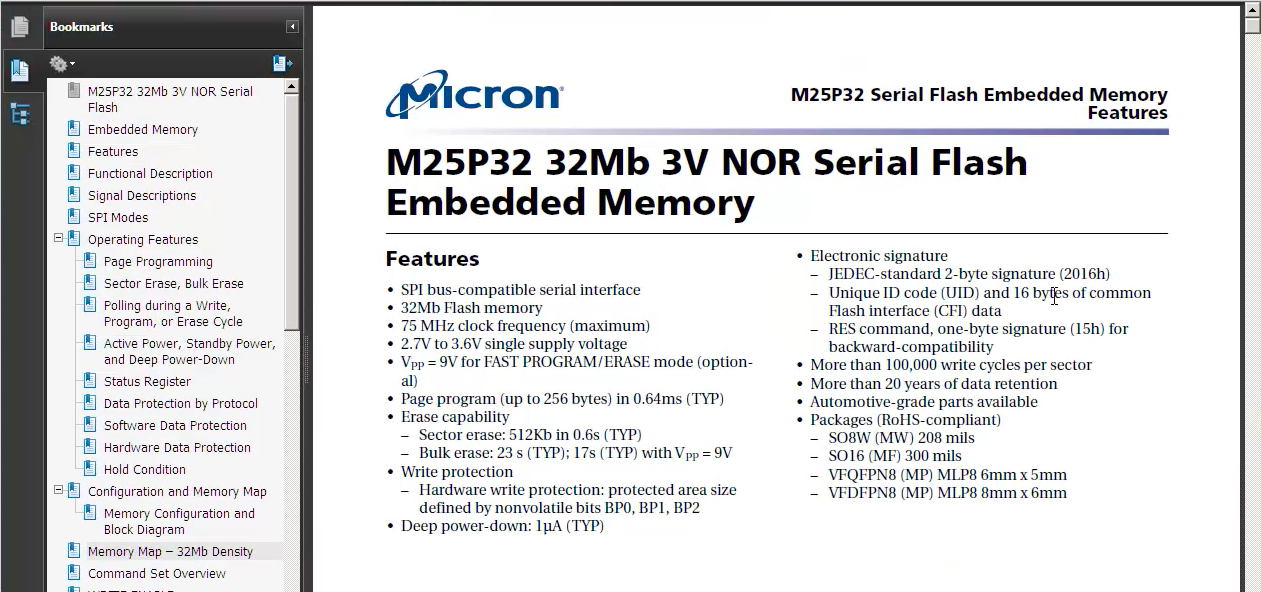
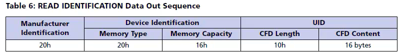
Its full identifier is 202016 - it is it that it returns in response to a command to request its code.
So everything is correct - the flash drive was found correct.
He tells us that there should be a file with the EPCS-202016 section.
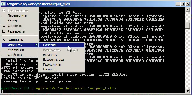
Wonderful. Edit - Mark. Select her name and take it to the clipboard.
We create the ovr.txt file and the section with the name that we just copied:

In the documentation for our flash drive, in the Memory Map section, we can see that it consists of 64 sectors. Each sector has a size of 64 KB, because from 0000 to FFFF.
Therefore, the configuration file that we just created should look like this:
64 sectors of 64 Kbytes in size, or 65536 bytes each.
The second step is ready. We have flasher.sof and ovr.txt files, which contains the flash drive configuration.
We pass to the third step.
Let me remind you that the working draft was USB16_my. And the file for the firmware was called Test1.sof. We copy flasher.sof and ovr.txt to it.
Now we have completed all the preparatory steps - we proceed to direct combat operations. To emphasize the lack of connection between preparation and work, I will enter the terminal again, as if it was happening the next day, one week, one month or any time after completion of preparation.
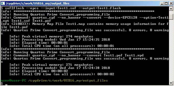
The first thing we need to do is generate an output file. Because the sof file is not sewn in the ROM - a slightly different file is sewn. In order to form it, we write:
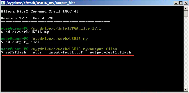
The file Test1.flash turned out:
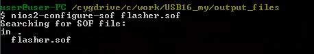
Now, purely formally, the turn has come to the actions that board builders should do. First of all, they should load our flasher in the same way, that is:
After which they should flash ROM:
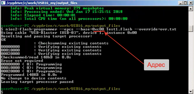
Actually, that’s all. The problem is solved, the flash drive is flashed - you can use it, even though the main path was talking about the mismatch of ID-schnicks. And you don’t have to buy expensive configurators or look for a vendor whose 25th flash drives have compatible IDs. We prepared the “flasher” for our specific board (and any others where the same chip is located and Reset with the generator are connected to the same output), we prepared a text file for the configurator, and then added the “firmware” using the utilities that come with the kit deliveries of the standard Quartus Prime environment (they also came with the Quartus II environment).
Details in the long text below. If it’s very interesting, but too lazy to read so many letters, you can simplify the task by watching a detailed 20-minute video.
So, back to our problem.
If you turn in your hands the very breadboard with a crystal of the Cyclone IV family, then we will see a very amazing thing.
Here it is, PLISina, and here is the configuration ROM:
Oddly enough, this is not EPCS, but the usual 25th flash drive. Such flash drives are cheap and sold quite a lot from anyone.
But as they say, not all yogurts are equally useful. In particular, our customers joyfully bought such flash drives, soldered on a board and got a global problem. We go into the programmer, load the file prepared for the firmware, start flashing it and get an error:
Here is the error message:
Error (209025): Can't recognize silicon ID for device 1. A device's silicon ID is different from its JTAG ID. Verify that all cables are securely connected, select a different device, or check the power on the target system. Make sure the device pins are connected and configured correctly.
The device identifier is not recognized. That is, the flash drive has an unknown identifier in terms of a quartus. Specifically, 25P32 crystals were purchased from our customers, which are generally not supported in principle, but there may be a more mundane situation in life. In particular, the ST flash drive is soldered in the photo above, and it is defined as MICRON. Chinese sellers and not so can mark, and when the batch is purchased and does not work - what can be done?
I climbed into the forums. All the Russian-speaking ones that were able to be inspected were full of discussions, which suppliers and what should be taken so as not to run into a similar problem. But in our case, no one wanted to buy a new batch. In English sources, only one article was found with a solution, but in the modern Quartus Prime environment, this solution will not work “head-on”. Therefore, we undertook to document this problem for the modern environment, in Russian and in video format.
So, how is ROM generally programmed?
A special configuration is poured into the FPGA, which makes it possible to tap through the JTAG to the flash drive. And then, using this configuration, we fill in the data. It turns out that you can make a similar configuration, which will give us access to the USB flash drive and allow us to flash it regardless of the ID, without having to write a single line of our own code, and the utilities will all be used from Quartus Prime (or Qiartus II, who uses old versions of the development environment).
That is, we have to take 3 steps:
- Make a configuration that knocks on a flash drive.
- Write the file in which the flash drive is described.
- To flash.
Let’s do it. Let's start by developing our own “firmware” (it’s the same configuration) without writing a single line of our code.
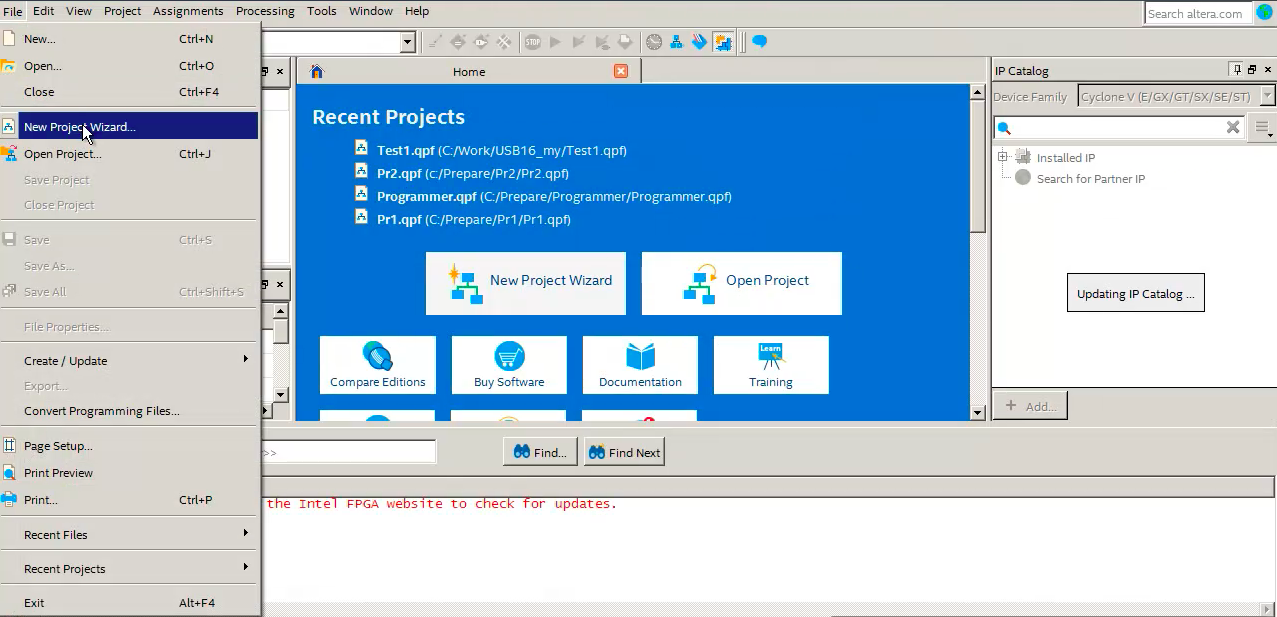
We go to Quartus:
We create a new project:
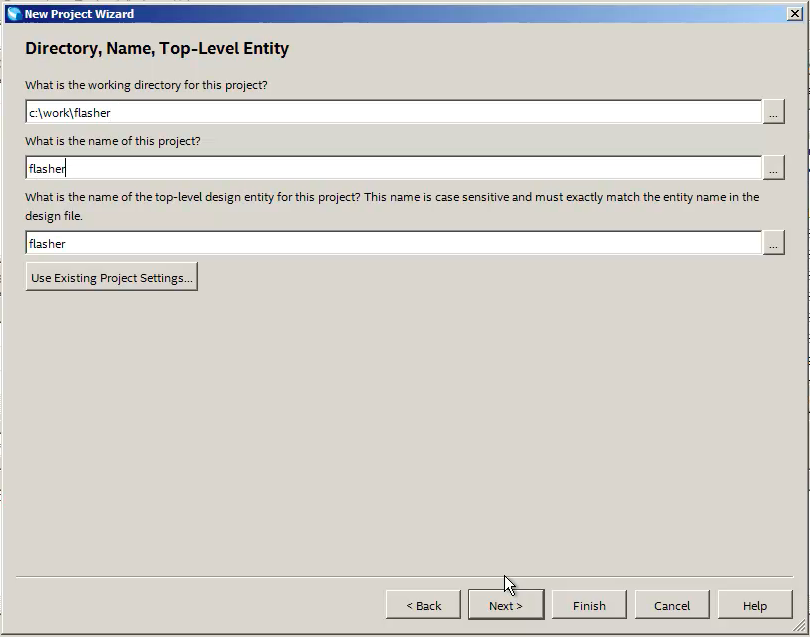
Let's
name it, say, flasher: This name should be remembered - we still need it.
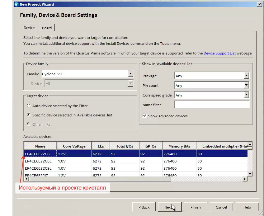
We create an empty project, my family is Cyclone IV E, the crystal used in the project is like this:
So. Finish creating the project, click Finish. The project is created. As already mentioned, we do not write a single line of our code. But you still need to get the environment to do something. To do this, go to Tools - Platform Designer.
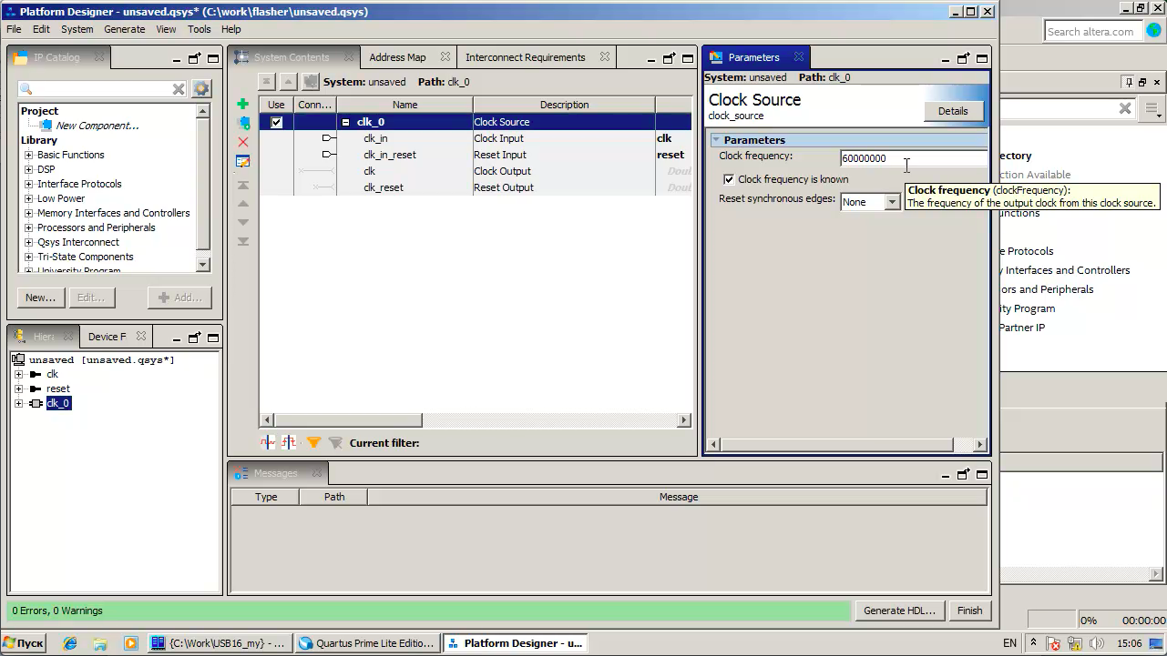
Here it booted. Specifically, I have 60 Hz quartz in this board, so I will correct the frequency settings:
What I do now, we do once for the platform. That is, if some kind of board is made, then this bootloader will work for it for any project.
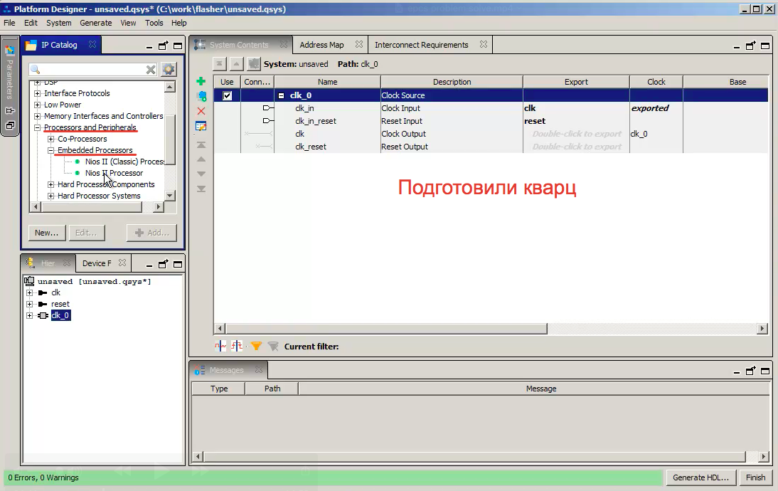
I prepared the quartz - now we put the processor. In the library on the left we find "Processors and Peripherals", "Embedded Processors" and then - Nios II Processor:
Select it and click "Add".
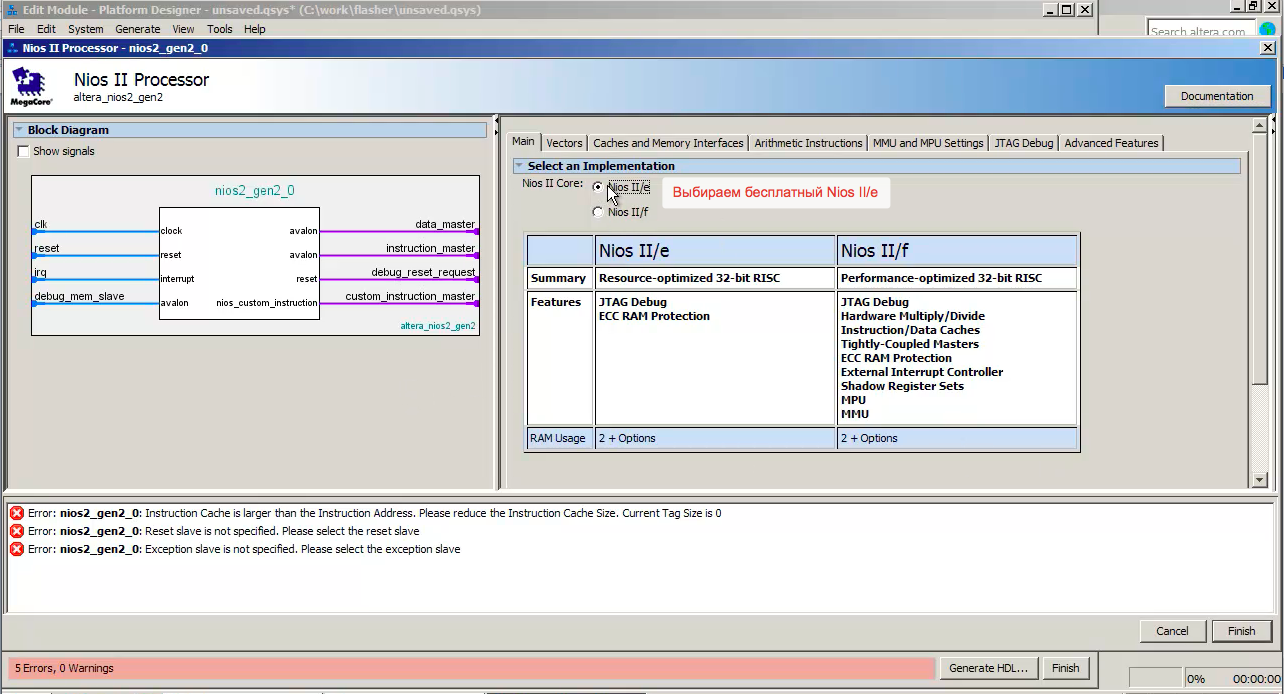
In the window that opens, in the properties, select Nios II / e, because it is absolutely free and it does not need any license.
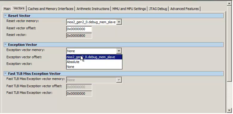
Errors tell us that the vectors are not configured. We are not going to program anything for this processor. Therefore, we simply direct the vectors to the first place from the list:
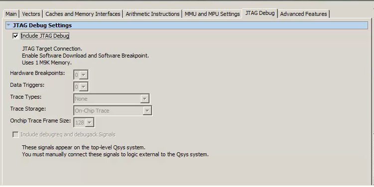
It is very important for us that the JTAG module works for the processor:
After our manipulations, the errors are gone.
With the processor over. Click Finish and move on.
Now we go to the main functions. There are configurators here: We
open the list of configurators - near the end we find EPCS - our configurators: We
leave everything by default:
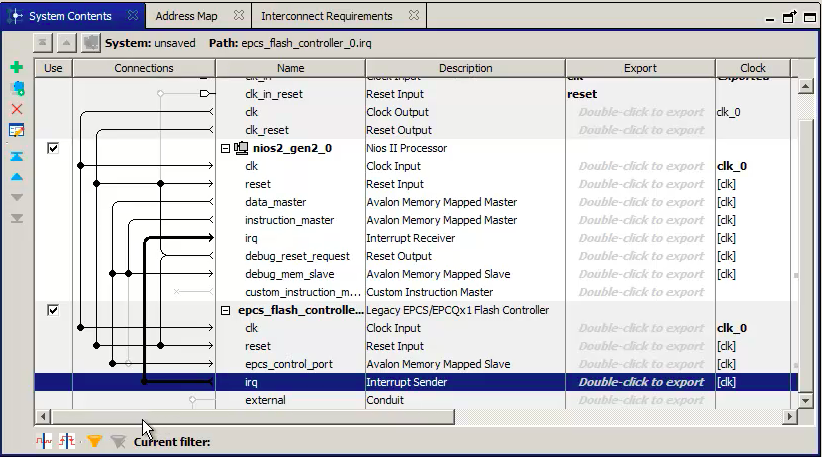
Now we begin to connect them. We pass the clock signals to both modules, we pass the reset signal to both modules. The reset signal coming out of the JTAG hardware - debug_reset_request - we also pass to both modules. Next, we skip data_master to both modules. Instruction_master is passed only to the debugger. And we also skip the interrupt request:
Next we go to the external legs - external. We export them, for which we double-click in the Double-click to export field:
For simplicity, I will call epcs so that the length is less:
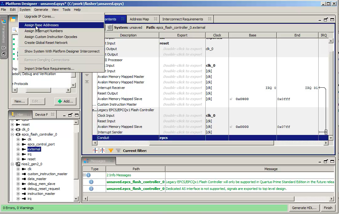
Now, with the usual hand movement, we assign the base addresses:
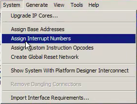
And we assign interrupts: The
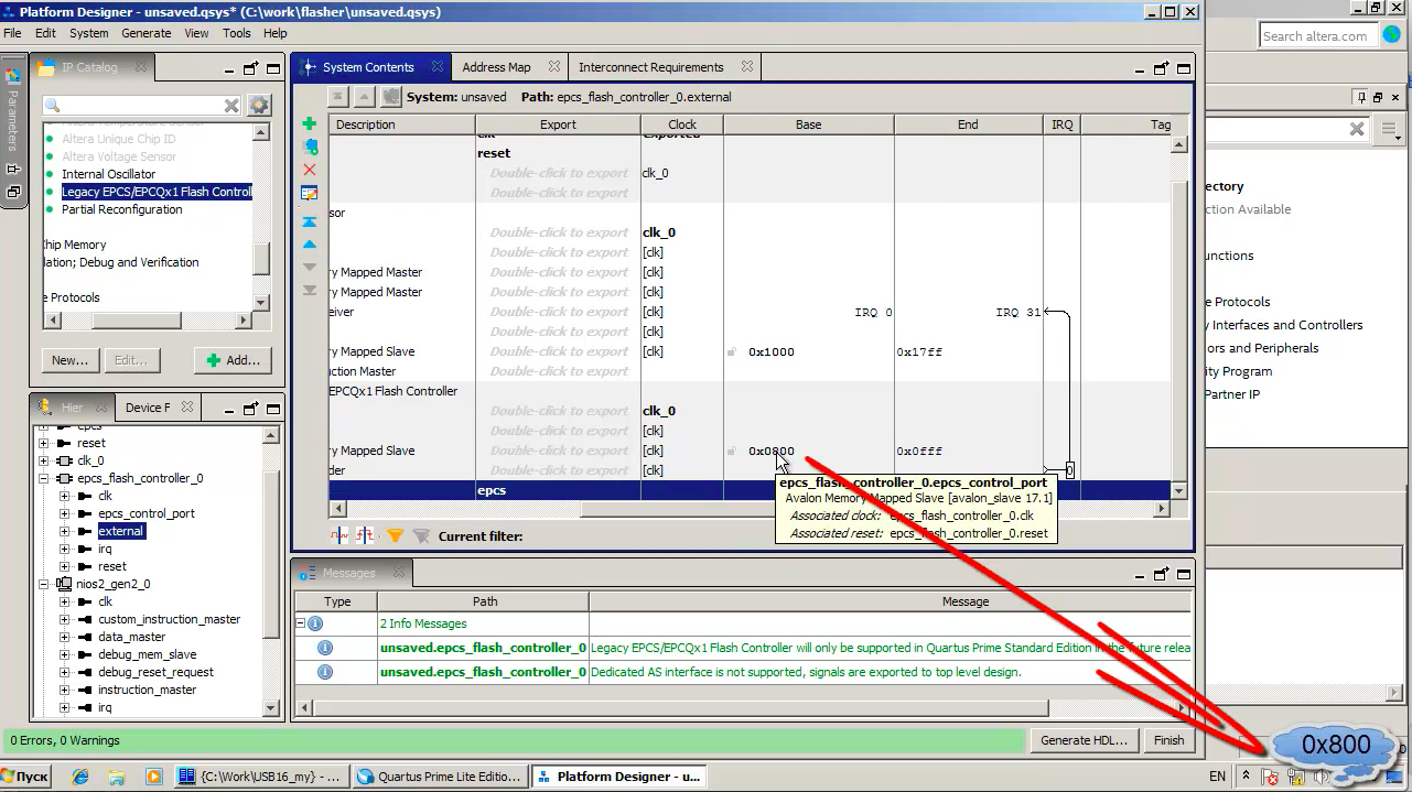
automatically assigned address for our flash controller is 0 × 800 - we should remember:
It will come in handy for us. And everything else, in principle, has done and will work.
Now it is very important, since we are not going to write a single line of our code so that the name of the processor system matches the name of the project. The project we had was flasher.
We save the system, call flasher:
It is then that the top module will have this particular processor, and therefore we will not have to do anything.
Our next step: We
leave everything by default, because we just use what is ready:
Finish:
There was a message that we need to remember to add the file to the project:
Let's add. Go to Project - Add / Remove Files in Project:
Find our file on the computer.
Here it is, our flasher file with the qsys extension.
Added it:
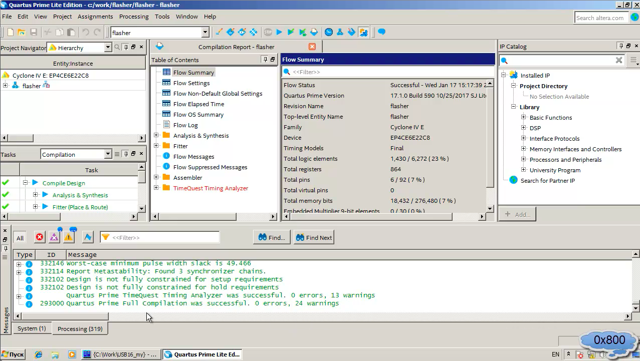
Now we are doing a rough compilation:
It completed successfully.
Now that she has passed, we can set conclusions. We go to the Pin Planner:
we don’t need to assign JTAG legs - we assign the legs of a flash drive.
For each chip, for each case they are different. In principle, you can look at the documentation on the chip or on your board. For example, here we have the twelfth leg of DCLK:
I have already prepared the list - just drive it.
So, epcs_data0, LOCATION: PIN13, epcs_dclk - PIN12, epcs_sce - PIN8, epcs_sdo - PIN6. And specifically on the board of our customers, the clock frequency is PIN24, reset_n - PIN88.
The legs are appointed. We start compilation. Errors are issued:
All because I pretended to forget to make a very important setting. We have now connected the USB flash drive to the service lines. And, at the end of the configuration, some of these lines are not available at all, and some are used for official purposes. Therefore, we were given messages that we have a conflict:
To resolve this, go to Assignments - Device:
Device and Pin Options:
Here we select Dual-Purpose Pins. And at the end of programming, we ask you to make all these lines the usual I / O lines:
Click OK, start the compiler. And it all worked out.
So, the first step is completed. We got a configuration through which we can tap to the flash drive.
Now our task is to create a file with which the system will recognize our USB flash drive.
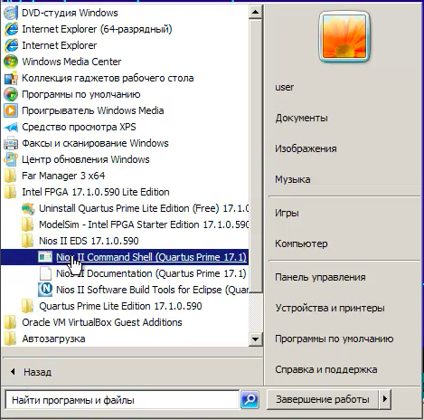
We go to all programs, Intel FPGA (for older versions it will be Altera), Nios II Command Shell.
Here we go to the directory where we just collected everything. At the same time, do not forget that the slashes here should not be reverse, but straight, and that the resulting flasher.sof file lies in the output_files directory:
Now we begin to cast magic spells. So, we need to inject the newly formed configuration. To do this, we write:
nios2-configure-sof flasher.sof
and press Enter:
The file is uploaded - now we have access to the flash drive. In order to determine everything regarding access to the flash drive, we need to run the following program:
nios2-flash-programmer --epcs --base = 0x800 - debug.
where 0x800 is the same address that was automatically assigned to the epcs block and which should not be forgotten.
Press Enter:
What did he tell us? He tried to inspect the area that we named. And at offset 0 at 800 I did not find anything. At address c00 he found what we needed:
Now we remember not just the base address 800, but the specific address c00 - in the future we will work with it.
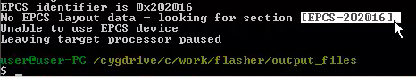
He found a flash drive, its identifier is 202016, but said that it has no idea what to do with it, because it does not know it.
Here is the documentation for our flash drive:
Its full identifier is 202016 - it is it that it returns in response to a command to request its code.
So everything is correct - the flash drive was found correct.
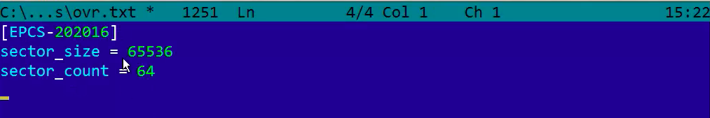
He tells us that there should be a file with the EPCS-202016 section.
Wonderful. Edit - Mark. Select her name and take it to the clipboard.
We create the ovr.txt file and the section with the name that we just copied:
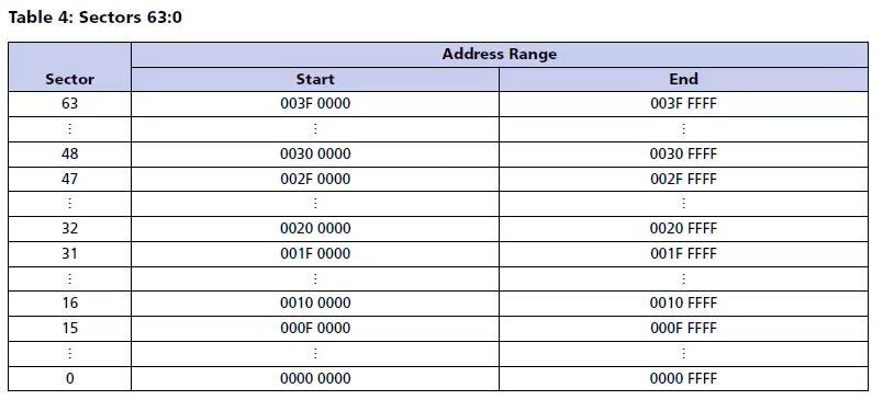
In the documentation for our flash drive, in the Memory Map section, we can see that it consists of 64 sectors. Each sector has a size of 64 KB, because from 0000 to FFFF.
Therefore, the configuration file that we just created should look like this:
64 sectors of 64 Kbytes in size, or 65536 bytes each.
The second step is ready. We have flasher.sof and ovr.txt files, which contains the flash drive configuration.
We pass to the third step.
Let me remind you that the working draft was USB16_my. And the file for the firmware was called Test1.sof. We copy flasher.sof and ovr.txt to it.
Now we have completed all the preparatory steps - we proceed to direct combat operations. To emphasize the lack of connection between preparation and work, I will enter the terminal again, as if it was happening the next day, one week, one month or any time after completion of preparation.
The first thing we need to do is generate an output file. Because the sof file is not sewn in the ROM - a slightly different file is sewn. In order to form it, we write:
The file Test1.flash turned out:
Now, purely formally, the turn has come to the actions that board builders should do. First of all, they should load our flasher in the same way, that is:
After which they should flash ROM:
Actually, that’s all. The problem is solved, the flash drive is flashed - you can use it, even though the main path was talking about the mismatch of ID-schnicks. And you don’t have to buy expensive configurators or look for a vendor whose 25th flash drives have compatible IDs. We prepared the “flasher” for our specific board (and any others where the same chip is located and Reset with the generator are connected to the same output), we prepared a text file for the configurator, and then added the “firmware” using the utilities that come with the kit deliveries of the standard Quartus Prime environment (they also came with the Quartus II environment).