Our methodology for calculating the stack of printed circuit boards
While we are finishing the final preparations for the serial production of the VESNIN server, I want to conduct an educational experiment - I will describe our internal methods and recommendations for calculating the stack of printed circuit boards. On the one hand, it is nice if our experience is useful to someone. On the other hand, we ourselves are pleased to receive sensible comments to improve our practice. If you are interested in reading and discussing, welcome to cat.
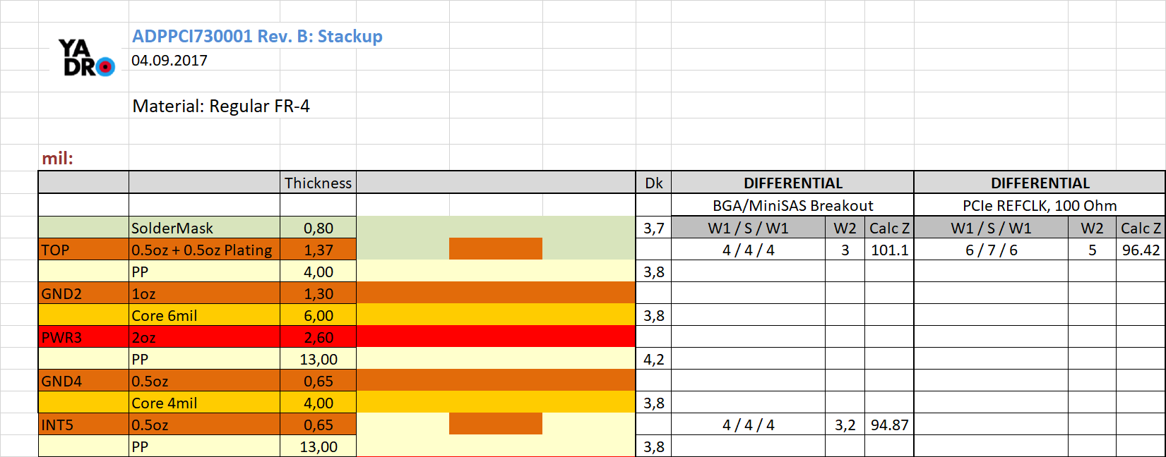
Immediately to the point - this is what is written in this article:
Everything described below is not Know How, but in fact, gathered together and systematized data from different sources. We do not claim absolute knowledge either.
So let's go.
Preamble (as usual).
Typically, an engineer roughly estimates the board stack, passes it to the PCB manufacturer. In response, he receives many Chinese letterheads with proposals - to which he usually agrees. They are reduced to changing the thickness of the cores / prepregs, as well as conductors and gaps in the CAM editor.
It is usually normal. But there are three minuses:
Therefore, we prefer to form the stack so that its dependence on the characteristics of a particular PCB manufacturer is minimized. If you are working with the same vendor, it is quite realistic to form a stack so that its modification by the manufacturer is not required at all. This saves 1-2 weeks in preparation for production.
By the way offtopic.
Surely someone will want to ask - which is better, tightly coupled or loosely coupled differential pairs. Our opinion: better loosely coupled - they are easier to align in length. You can afford more serious bumps. From the point of view of SI, in our opinion, there are no special advantages of strongly coupled pairs over weakly coupled (if we do not consider strange topologies of type 5-14-5). For lovers of formal rules: one or two widths between conductors in pairs is normal. More - not so much. Less is hard to align. Despite the fact that EMC indicators of strongly coupled pairs are much better, in absolute terms this “strongly” is not significant.
In order to more or less accurately form a stack of a printed circuit board, you need to know the parameters of specific cores and prepregs of the material used. The datasheets give the average parameters for the entire group and for accurate calculation these data are not suitable. This information can be requested from both the material manufacturer and the PCB manufacturer. This is a table that looks something like this (each material manufacturer has its own): The


thicknesses of different types of prepregs are usually the same for different manufacturers. Therefore, the information in the above picture is relevant and usable regardless of the manufacturer of the material (Dk / Df, of course, everyone has a different one).
When designing the PCB stack, it is necessary to take into account that PCB manufacturers, as a rule, make adjustments for lamination, reducing the dielectric constant (Dk) of both prepregs and cores by about 0.2 relative to the values given in the materials manufacturer's documentation.
If the Dk / Df values are given for different frequencies, it is recommended to use the values of these parameters for the frequency closest to the Nyquist frequency of the fastest interface on the PCB. For example, if PCI Express Gen3 is present on the PCB, then Dk / Df should be used for the frequency closest to 4 GHz.
Someone will object: how, after all, the band of the same Gen3 extends right up to 18 GHz. That's true - but the PCIe specification governs RL and IL until Nyquist, and all these hellish gigahertz won't go through the connectors, vias, and the circuit board - they fade out along the way. And if they pass, it is a big question whether you will like the result.
In a situation where there are several different high-speed interfaces on the PCB, you should not use the Dk / Df values for different frequencies within the stack of one board. Despite the fact that this approach is more correct from the point of view of impedance calculation, it will cause great difficulties in coordinating the stack with the PCB manufacturer (their test equipment is tuned to one specific frequency).
If the values of Dk / Df vary significantly with the frequency, and the impedance control is critical, it makes sense to get the impedance for the real frequency of the interface, recalculate it by taking Dk for a single frequency (the most critical interface). The impedance value “normalized” in this way should be indicated as the target for the PCB manufacturer's control.
For example, you calculate 100 Ohm path for a frequency of 4 GHz, use the Dk value for 4 GHz, and trace in accordance with the data received. Further, if for example you have interfaces that require calculation for 10 GHz, substitute the Dk value for a higher frequency in the original calculation. Suppose you get an impedance value of 105 ohms. Our tip: here are 105 ohms and tell the PCB manufacturer for control. Do not fool him with different Dk for different frequencies on the same layer.
It also doesn’t hurt to ask on the glass with which the fab works on the shore, so that later there would be no problems with the delivery time. Because there are popular prepregs and not really. Usually in the warehouse he always has enough of 3-4 types, from which it is worth building a PCB stack. Materials with low losses usually do not exist in the warehouse, due to the limited shelf life - therefore, the use of something special is always a matter of not so much price, but production time.
The table below shows the absolute values of the change in the thickness of one layer of the prepreg for different application conditions. The tolerance on all values is 10%.
For a more accurate calculation of the change in the thickness of the prepreg, you can use the following expression:
In the case where one prepreg layer is located between the metallization layers, the values of the thickness changes for the respective conditions should be summed up, since the change in the thickness of the prepreg is actually an indentation of the conductive pattern into it.
When forming a layered description of the PCB, the final value of the prepreg should be indicated. At the same time, a portion of the prepreg pressed into the metallization pattern should not be included in the value of the finishing thickness in the documentation transmitted to the PCB manufacturer.

It is necessary to calculate the finishing thickness of the stack shown in the figure. Copper 1 oz is used on all metallization layers. The initial thickness of the prepreg 2116 is 5.1 mil.

The resulting stack will look like:
The expression for calculating the Etch Factor for the process of electric deposition of copper is shown in the figure:

The table shows the Etch Factor values for different types of metallization for different manufacturers. As you can see, they are very different. Therefore, the value of EF is the first thing you should check with your PCB partner.
For cases when there is no information on the value of EF from a particular production, we can assume that EF takes the following values:
When calculating the metallization of the outer layers, the value of the thickness of copper weighing 1 oz, as a rule, is assumed to be 1.37 mil. It is recommended to separately set the weight of the base copper and the weight of the deposited copper. The final value is obtained by summing these two parameters. Typical values are given in the table:
For the inner layers, the value of the thickness of copper weighing 1 oz, as a rule, is assumed to be 1.3 mil.
When taking into account the solder mask, we rely on the following scheme:

In cases where it is not explicitly indicated otherwise, we can assume that the solder mask has the following parameters:
Most manufacturers, when considering the influence of the solder mask, consider the values C1, C2 and C3 equal to each other.
Some factories consider C1 and C3 to be equal to the metallization thickness (T1), and C2 to 0.8 mil. The correctness of this approach is approximately confirmed by real data obtained after PCB production.
One of our PCB partners considers the thickness of the solder mask on solid sections of copper 0.79 - 1.18 mil, on the edges of the conductors 0.2 mil. Also, this manufacturer, when calculating the stack, recommends not including the solder mask in the calculation, since when etching the outer layers, there is the slightest grinding (that is, an increase in the impedance value), which is compensated by the mask to the nominal value of the theoretical impedance measurement of the outer layers without a mask.
This, by the way, is a good example of the fact that when working with this production, the thickness of the tracks on your PCB will be less than that laid down in the circuit board design.
These are our internal recommendations and rules, with which we are obligatorily familiar with all engineers designing printed circuit boards. I hope that this article will be useful to those who scour the Internet for scattered recommendations and try to guess how it will turn out in his particular product. I invite you to share your experience in the comments - we will be glad to supplement yours. If there is interest, I will post a few more of these internal instructions.
- PCB Materials
- Accounting for changes in prepreg thickness during PCB manufacturing
- Accounting Etch Factor
- Features of calculating the thickness of metallization
- Accounting for solder mask
Everything described below is not Know How, but in fact, gathered together and systematized data from different sources. We do not claim absolute knowledge either.
So let's go.
PCB Materials
Preamble (as usual).
Typically, an engineer roughly estimates the board stack, passes it to the PCB manufacturer. In response, he receives many Chinese letterheads with proposals - to which he usually agrees. They are reduced to changing the thickness of the cores / prepregs, as well as conductors and gaps in the CAM editor.
It is usually normal. But there are three minuses:
- The final product is different from what is described in your CD (sometimes a little more than completely).
- There is no repeatability of the result when switching to another manufacturer. For example, we have a board that was launched on two different fabs with completely different stacks (in this case, the initial data in both cases were the same).
- If the thickness of the conductors on the printed circuit board is in the zone of 4 mil, then any change in their width in the direction of reduction very seriously affects the loss. If the difference between the conductor 6 mil and 5 mil is insignificant, then between 5 mil and 4 mil it is very significant, and 4 mil and 3 mil are different universes from the point of view of losses. (In general, in our opinion, the ideal topologies of a differential pair are 6-6-6 or 7-7-7).
Therefore, we prefer to form the stack so that its dependence on the characteristics of a particular PCB manufacturer is minimized. If you are working with the same vendor, it is quite realistic to form a stack so that its modification by the manufacturer is not required at all. This saves 1-2 weeks in preparation for production.
By the way offtopic.
Surely someone will want to ask - which is better, tightly coupled or loosely coupled differential pairs. Our opinion: better loosely coupled - they are easier to align in length. You can afford more serious bumps. From the point of view of SI, in our opinion, there are no special advantages of strongly coupled pairs over weakly coupled (if we do not consider strange topologies of type 5-14-5). For lovers of formal rules: one or two widths between conductors in pairs is normal. More - not so much. Less is hard to align. Despite the fact that EMC indicators of strongly coupled pairs are much better, in absolute terms this “strongly” is not significant.
In order to more or less accurately form a stack of a printed circuit board, you need to know the parameters of specific cores and prepregs of the material used. The datasheets give the average parameters for the entire group and for accurate calculation these data are not suitable. This information can be requested from both the material manufacturer and the PCB manufacturer. This is a table that looks something like this (each material manufacturer has its own): The
thicknesses of different types of prepregs are usually the same for different manufacturers. Therefore, the information in the above picture is relevant and usable regardless of the manufacturer of the material (Dk / Df, of course, everyone has a different one).
When designing the PCB stack, it is necessary to take into account that PCB manufacturers, as a rule, make adjustments for lamination, reducing the dielectric constant (Dk) of both prepregs and cores by about 0.2 relative to the values given in the materials manufacturer's documentation.
If the Dk / Df values are given for different frequencies, it is recommended to use the values of these parameters for the frequency closest to the Nyquist frequency of the fastest interface on the PCB. For example, if PCI Express Gen3 is present on the PCB, then Dk / Df should be used for the frequency closest to 4 GHz.
Someone will object: how, after all, the band of the same Gen3 extends right up to 18 GHz. That's true - but the PCIe specification governs RL and IL until Nyquist, and all these hellish gigahertz won't go through the connectors, vias, and the circuit board - they fade out along the way. And if they pass, it is a big question whether you will like the result.
In a situation where there are several different high-speed interfaces on the PCB, you should not use the Dk / Df values for different frequencies within the stack of one board. Despite the fact that this approach is more correct from the point of view of impedance calculation, it will cause great difficulties in coordinating the stack with the PCB manufacturer (their test equipment is tuned to one specific frequency).
If the values of Dk / Df vary significantly with the frequency, and the impedance control is critical, it makes sense to get the impedance for the real frequency of the interface, recalculate it by taking Dk for a single frequency (the most critical interface). The impedance value “normalized” in this way should be indicated as the target for the PCB manufacturer's control.
For example, you calculate 100 Ohm path for a frequency of 4 GHz, use the Dk value for 4 GHz, and trace in accordance with the data received. Further, if for example you have interfaces that require calculation for 10 GHz, substitute the Dk value for a higher frequency in the original calculation. Suppose you get an impedance value of 105 ohms. Our tip: here are 105 ohms and tell the PCB manufacturer for control. Do not fool him with different Dk for different frequencies on the same layer.
It also doesn’t hurt to ask on the glass with which the fab works on the shore, so that later there would be no problems with the delivery time. Because there are popular prepregs and not really. Usually in the warehouse he always has enough of 3-4 types, from which it is worth building a PCB stack. Materials with low losses usually do not exist in the warehouse, due to the limited shelf life - therefore, the use of something special is always a matter of not so much price, but production time.
Accounting for changes in prepreg thickness during PCB manufacturing
The table below shows the absolute values of the change in the thickness of one layer of the prepreg for different application conditions. The tolerance on all values is 10%.
| Conditions | Change in prepreg thickness at initial value | |
|---|---|---|
| No more than 2.3 mil | More than 2.3 mil | |
| Copper 0.5 oz with 30% coverage | 0.4 mil | 0.4 mil |
| Copper 0.5 oz with 70% coverage | 0.1 mil | 0.2 mil |
| Copper 1 oz with 30% coverage | 0.8 mil | 0.9 mil |
| Copper 1 oz with 70% coverage | 0.3 mil | 0.4 mil |
| Adhesion to copper 2 oz with 30% coverage | 1.8 mil | 1.9 mil |
| Adhesion to copper 2 oz with 70% coverage | 0.8 mil | 0.8 mil |
| Located between two layers of prepreg | 9% | 10% |
| Adhesion to the outer layer | does not change | does not change |
For a more accurate calculation of the change in the thickness of the prepreg, you can use the following expression:

In the case where one prepreg layer is located between the metallization layers, the values of the thickness changes for the respective conditions should be summed up, since the change in the thickness of the prepreg is actually an indentation of the conductive pattern into it.
When forming a layered description of the PCB, the final value of the prepreg should be indicated. At the same time, a portion of the prepreg pressed into the metallization pattern should not be included in the value of the finishing thickness in the documentation transmitted to the PCB manufacturer.
Example
It is necessary to calculate the finishing thickness of the stack shown in the figure. Copper 1 oz is used on all metallization layers. The initial thickness of the prepreg 2116 is 5.1 mil.
The resulting stack will look like:
| Layer type | Initial thickness | Thickness change | Finish thickness |
|---|---|---|---|
| External | 1.35 mil | - | 1.35 mil |
| Layer 2116 | 5.1 mil | - | 5.1 mil |
| Layer 2116 | 5.1 mill | 0.9 mil | 4.2 mil |
| Internal alarm | 1.35 mil | - | 1.35 mil |
| Core | 39 mil | - | 39 mil |
| Inner plane | 1.35 mil | - | 1.35 mil |
| Layer 2116 | 5.1 mil | 0.4 mil | 4.7 mil |
| Layer 2116 | 5.1 mil | - | 5.1 mil |
| External | 1.35 mil | - | 1.35 mil |
| Total: | 63.5 mil ± 10% |
Accounting Etch Factor
The expression for calculating the Etch Factor for the process of electric deposition of copper is shown in the figure:
The table shows the Etch Factor values for different types of metallization for different manufacturers. As you can see, they are very different. Therefore, the value of EF is the first thing you should check with your PCB partner.
| Layer type | Factory 1 | Factory 2 | Factory 3 | Factory 4 | ||||
|---|---|---|---|---|---|---|---|---|
| Ef | W2-w1 | Ef | W2-w1 | Ef | W2-w1 | Ef | W2-w1 | |
| External 0.5 oz | 3.4 - 4 | 1 mil | 3.4 - 4 | 1 mi | 3.4 - 2 | 1.5 mil | 2.6 | - |
| External 1 oz | - | - | - | - | 1.66 | 2.4 mil | 2.6 | - |
| Internal 0.5 oz | 1.75 | 0.8 mil | 4.33 | 0.3 mil | 1.73 | 1.75 mil | 3 | - |
| Inner 1 oz | 2.4 | 1 mil | 4.33 | 0.6 mil | 2.6 | 1 mil | 3 | - |
| Inner 2 oz | - | 1.5 - 2 mil | 4.33 | 1.2 mil | 2.6 | 2 mil | 3 | - |
| Inner 3 oz | - | - | - | - | 2.6 | 3 mil | 3 | - |
| Inner 4 oz | - | - | - | - | 2.3 | 4.5 mil | 3 | - |
For cases when there is no information on the value of EF from a particular production, we can assume that EF takes the following values:
- outer layers - 2.6
- inner layers - 3.7
Features of calculating the thickness of metallization
Metallization of the outer layers
When calculating the metallization of the outer layers, the value of the thickness of copper weighing 1 oz, as a rule, is assumed to be 1.37 mil. It is recommended to separately set the weight of the base copper and the weight of the deposited copper. The final value is obtained by summing these two parameters. Typical values are given in the table:
| Base copper | Plating copper | ||
|---|---|---|---|
| 0.7oz | 1oz | 2oz | |
| 0.5oz | 1.644 mil | 2.055 mil | 3.425 mil |
| 1oz | 2.329 mil | 2.74 mil | 4.11 mil |
| 2oz | 3.699 mil | 4.11 mil | 5.48 mil |
| 3oz | 5.069 mil | 5.48 mil | 6.85 mil |
Metallization of the inner layers
For the inner layers, the value of the thickness of copper weighing 1 oz, as a rule, is assumed to be 1.3 mil.
Accounting for solder mask
When taking into account the solder mask, we rely on the following scheme:
In cases where it is not explicitly indicated otherwise, we can assume that the solder mask has the following parameters:
- Dk - 3.7
- Df - 0.025
- Thickness - 0.8 mil
Most manufacturers, when considering the influence of the solder mask, consider the values C1, C2 and C3 equal to each other.
Some factories consider C1 and C3 to be equal to the metallization thickness (T1), and C2 to 0.8 mil. The correctness of this approach is approximately confirmed by real data obtained after PCB production.
One of our PCB partners considers the thickness of the solder mask on solid sections of copper 0.79 - 1.18 mil, on the edges of the conductors 0.2 mil. Also, this manufacturer, when calculating the stack, recommends not including the solder mask in the calculation, since when etching the outer layers, there is the slightest grinding (that is, an increase in the impedance value), which is compensated by the mask to the nominal value of the theoretical impedance measurement of the outer layers without a mask.
This, by the way, is a good example of the fact that when working with this production, the thickness of the tracks on your PCB will be less than that laid down in the circuit board design.
Summary
These are our internal recommendations and rules, with which we are obligatorily familiar with all engineers designing printed circuit boards. I hope that this article will be useful to those who scour the Internet for scattered recommendations and try to guess how it will turn out in his particular product. I invite you to share your experience in the comments - we will be glad to supplement yours. If there is interest, I will post a few more of these internal instructions.