A tour of the Computer History Museum in California, with usefulness for development. Part 1. ENIAC, Stretch, CDC6600, IBM / 360
Lord! Today we will walk with a Siberian girl Irina at the Computer History Museum in Mountain View, California. And we’ll walk not as tourists, but for the benefit of Russia. I already wrote in a previous post that one of the effective ways for a student to study the design of processors is to take some ancient, but instructive processor, find documentation on its architecture (and some information on its microarchitecture), and design an analogue of this processor in the language of the SystemVerilog hardware description (or VHDL, if you like it more), and then implement the processor on the FPGA / FPGA board (which one, it doesn’t matter - Altera / Intel FPGA, Xilinx or Lattice). As a tutorial for this exercise, you can start with Harris & Harris , and then continue withbooks for a more advanced learning phase, such as Shen Lipasti .
How will all this benefit Russia? For such projects, we are going to distribute FPGA boards at a conference which will be held on September 18-22 in Tomsk . Representatives of Moscow State University, Moscow Institute of Physics and Technology, MIET, ICST, Imagination Technologies, National Instruments, etc. will come there. They will discuss how to update the university curriculum so that today's students will design Russian chips in a few years at the level of leading Western companies. There will also be a school seminar where they will discuss how to make educational processors - starting from the simplest schoolMIPS from Stanislav Zhelnio sparf .
Here is the first photo from the museum in Mountain View - in addition to Irina and a rocket, a small box is visible in it in the center. This is the on-board computer of the MIR space station , which was designed by engineers of the Soviet ELAS association, which was transformed into the modern ELVIS company Zelenograd :

So, topics for training projects are starting from the dense decades of the middle of the 20th century:
Before us is a block for storing the table of results of calculating the arithmetic functions of a warm ENIAC tube computer, developed in 1943-1947 by Presper Eckert and John Mauchly of the University of Pennsylvania. At some point, their colleague John von Neumann suggested using this block to store programs. Thus was born the "architecture of von Niemen." In general, it would be correct to call it "Eckert-Mauchly-von-Neumann architecture", but Eckert and Mauchly were unlucky - their names were kept secret, and the name of von-Neumann was not (the computer was intended for calculating artillery tables).
If you want to implement this computer on FPGA, I googled ENIAC_Operating_Manual , although it will not be trivial to turn it into code on a veril:
Transistor supercomputer IBM 7030 Stretch. The name (stretch - “stretch”) came from the promise of its creators to make the computer 100 times faster than the previous IBM 704. Unfortunately, Stretch turned out to be only 30 times faster and the business community covered the creators with shame and contempt. However, in the process of this “failure”, the IBM engineers came up with pipelines, multitasking, and memory protection:
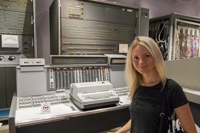
CDC 6600 (1963). The first "real" supercomputer in history and the first processor with extraordinary execution of instructions. Still widely used as an example, scoreboarding in lectures on microarchitecture (see, for example, the first google (though not very fresh) CDC 6600 slides from Berkeley) Implementation of a simplified CDC 6600 on a veril and FPGA is one of the most obvious candidates for a student coursework project.

Here is an excerpt about the general organization of the CDC 6600 from Microprocessor Architecture: From Simple Pipelines to Chip Multiprocessors by Jean-Loup Baer (2009). Several functional devices running in parallel (but without a pipeline) and a scoreboard that tracks data dependencies between instructions and pauses the execution of an instruction until its operands are ready:

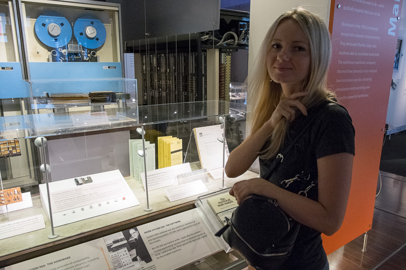
IBM 360 (1964-1978). This line of computers made such a deep impression on the Central Committee of the CPSU of the USSR that, despite the resistance of Soviet supercomputer authorities from ITMiVT (BESMs and Elbrus), they planted Soviet implementations of IBM 360/370 across all social countries under the name of EU computer. These computers are even depicted in drawings by Soviet children of the Brezhnev era “I’m at my mother’s work”:

In principle, there was a reason - the IBM / 360 line introduced a revolutionary concept for its time: “unified architecture (command system) - different microarchitectural implementations (conveyor devices and the structure of hardware blocks)”. In other words, the same software could work on both slow, cheap and fast expensive computers of this line - without recompilation. (True, the software for these machines was not very friendly compared to the software on the soon emerging minicomputers, but IBM hardware engineers were not to blame for this, it was the fault of IBM programmers and their management).
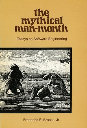
However, the IBM / 360 project has also benefited the programming world. Do you see the book Mythical Man-Month by Frederick Brooks to the left of Irina’s handbag? The author of the book is the OS / 360 project manager, who made the observation that an attempt to fix a broken deadline by adding new programmers to the project often leads to a worse situation - the deadline will become even more frustrated. The book was published in 1975, was immediately transferred to the USSR, and in some places it is still relevant:
The IBM / 360 line also introduced into the mainstream the concept of “microprogramming” and “microcode”, which became irrelevant during the “RISC revolution” of the 1980s (modern microprocessors are mostly hardwired due to the need to convey everything). However, these concepts have become so ingrained in Soviet and post-Soviet computer architecture textbooks that people still ask the question “what, Verilog is microprogramming?” - after which it takes a long time to explain that it is _not_ microprogramming.
So why implement IBM / 360 on FPGA? It is pointless to implement everything, but one aspect of one model, namely the IBM System / 360 Model 91, appears among modern student coursework projects on microarchitecture no less than the scoreboard from the CDC 6600. I am talking about the so-called “Tomasulo algorithm”, a way of organizing an extraordinary execution arithmetic operations with hardware "renaming of registers" and "reservation blocks" (yes, these things are also in the processors in your iPhones, these are not the remains of a mammoth). It is rather strange that there is no article on the Tomasulo algorithm on the Russian Wikipedia, although there is on the Ukrainian:
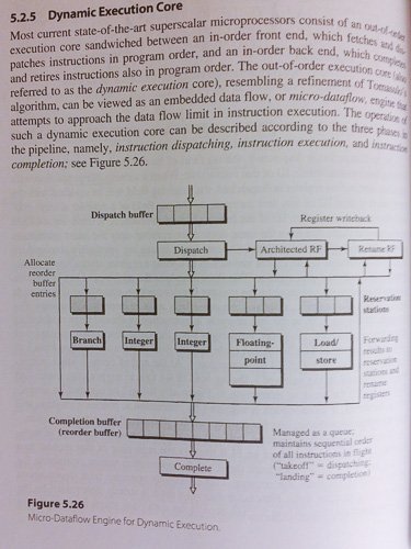
One of the most useful modern books on processor development, Modern Processor Design: Fundamentals of Superscalar Processors by John Paul Shen and Mikko H. Lipasti (2013), illustrates how IBM / 360-91's floating point block looked like before Tomasulo and after him. The same “before and after” can be done for a student project, by comparing performance (the number of clock cycles in different sequences of operations) and maximum clock frequency (when implemented on FPGA):

After that, the book of Shen-Lipasti describes how this is done in modern processors with dynamic conveyor:
And here is the early transistor mainframe from Japan - NEAC 2203, made in 1958. It was never sold outside of Japan. In general, then there was a frivolous attitude towards Japanese goods in the world, but Japanese companies suppressed idolatry in the West and engaged in Japanese capitalism. First, they tested technological solutions in the domestic market (a kind of “import substitution”), and then they aggressively attacked the world market. After a couple of decades, Japan ousted American companies from the market of memory chips and home electronics, and the same NEC built the most powerful supercomputer in 1992 - NEC SX-3/44. At the same time, voices began to appear in Japan about the need to reduce political dependence on the United States, and the Japanese Minister of Transport wrote a book 「NO」 と 言 え る «(“ Japan can say “NO”!). Unfortunately,

This concludes the first part of a walk through the museum. If you liked the beginning, I can write more about Cray and Illiac supercomputers, HP mini-computers, DEC and Data General, the first microprocessors and microcomputers, RISC workstations and Lisp machines, game consoles and robots.
Now we recall what all of this is for:
If you are interested in open-source projects of this type to increase public education, you are ready to write them on SystemVerilog or VHDL, upload code on GitHub and write articles about them on Habré (with performance analysis), but you don’t have an FPGA board - you can lend her (and get it permanently if the project is successful) in one of three places:
1. Alexander Romanov from HSE MIEM in Moscow. Alexander introduces Verilog courses for students, and in addition to regular boards, the university has a diverse collection of boards with Altera and Xilinx FPGA, both commonly used boards from Terasic and Digilent, as well as poorly documented Chinese boards - for open source projects.
2. Yaroslav Wozniuk from the Kiev-Mohyla Academy. I came to their hackathon for schoolchildren, and left there several Digilent Cmod A7 35T boards with Xilinx Artix-7 for barter “project fee with an article on Habré”.
3. Vladimir Makukha from Novosibirsk Technical State University. There is a set of boards for the conference in Tomsk, which is going through a week . Some of them (Digilent Nexys DDR4) will remain with Vladimir, some (Terasic DE0-CV) will go to such projects.
As an inspiration, you can look at existing projects with FPGA-based processors on Habr from SparF , Frantony , oleh_plotnikov , Kingit , VMSS , kirill90 , Boris_92 (you can add yours in the comments).
Ancient processors were made of radio tubes, transistors, microcircuits of a small degree of integration and drawing circuits with the mouse on the screen. Now all this is not so. A few words for those readers who are not familiar with what Verilog, ASIC and FPGA are:
From a post on Geektimes »Microelectronics squires . Video from the San Francisco Electronics Design Conference :
From a post on Habrahabr How to start developing iron using FPGAs - step by step instructions :
How will all this benefit Russia? For such projects, we are going to distribute FPGA boards at a conference which will be held on September 18-22 in Tomsk . Representatives of Moscow State University, Moscow Institute of Physics and Technology, MIET, ICST, Imagination Technologies, National Instruments, etc. will come there. They will discuss how to update the university curriculum so that today's students will design Russian chips in a few years at the level of leading Western companies. There will also be a school seminar where they will discuss how to make educational processors - starting from the simplest schoolMIPS from Stanislav Zhelnio sparf .
Here is the first photo from the museum in Mountain View - in addition to Irina and a rocket, a small box is visible in it in the center. This is the on-board computer of the MIR space station , which was designed by engineers of the Soviet ELAS association, which was transformed into the modern ELVIS company Zelenograd :
So, topics for training projects are starting from the dense decades of the middle of the 20th century:
Before us is a block for storing the table of results of calculating the arithmetic functions of a warm ENIAC tube computer, developed in 1943-1947 by Presper Eckert and John Mauchly of the University of Pennsylvania. At some point, their colleague John von Neumann suggested using this block to store programs. Thus was born the "architecture of von Niemen." In general, it would be correct to call it "Eckert-Mauchly-von-Neumann architecture", but Eckert and Mauchly were unlucky - their names were kept secret, and the name of von-Neumann was not (the computer was intended for calculating artillery tables).
If you want to implement this computer on FPGA, I googled ENIAC_Operating_Manual , although it will not be trivial to turn it into code on a veril:
Transistor supercomputer IBM 7030 Stretch. The name (stretch - “stretch”) came from the promise of its creators to make the computer 100 times faster than the previous IBM 704. Unfortunately, Stretch turned out to be only 30 times faster and the business community covered the creators with shame and contempt. However, in the process of this “failure”, the IBM engineers came up with pipelines, multitasking, and memory protection:
CDC 6600 (1963). The first "real" supercomputer in history and the first processor with extraordinary execution of instructions. Still widely used as an example, scoreboarding in lectures on microarchitecture (see, for example, the first google (though not very fresh) CDC 6600 slides from Berkeley) Implementation of a simplified CDC 6600 on a veril and FPGA is one of the most obvious candidates for a student coursework project.
Here is an excerpt about the general organization of the CDC 6600 from Microprocessor Architecture: From Simple Pipelines to Chip Multiprocessors by Jean-Loup Baer (2009). Several functional devices running in parallel (but without a pipeline) and a scoreboard that tracks data dependencies between instructions and pauses the execution of an instruction until its operands are ready:
IBM 360 (1964-1978). This line of computers made such a deep impression on the Central Committee of the CPSU of the USSR that, despite the resistance of Soviet supercomputer authorities from ITMiVT (BESMs and Elbrus), they planted Soviet implementations of IBM 360/370 across all social countries under the name of EU computer. These computers are even depicted in drawings by Soviet children of the Brezhnev era “I’m at my mother’s work”:
In principle, there was a reason - the IBM / 360 line introduced a revolutionary concept for its time: “unified architecture (command system) - different microarchitectural implementations (conveyor devices and the structure of hardware blocks)”. In other words, the same software could work on both slow, cheap and fast expensive computers of this line - without recompilation. (True, the software for these machines was not very friendly compared to the software on the soon emerging minicomputers, but IBM hardware engineers were not to blame for this, it was the fault of IBM programmers and their management).
However, the IBM / 360 project has also benefited the programming world. Do you see the book Mythical Man-Month by Frederick Brooks to the left of Irina’s handbag? The author of the book is the OS / 360 project manager, who made the observation that an attempt to fix a broken deadline by adding new programmers to the project often leads to a worse situation - the deadline will become even more frustrated. The book was published in 1975, was immediately transferred to the USSR, and in some places it is still relevant:
The IBM / 360 line also introduced into the mainstream the concept of “microprogramming” and “microcode”, which became irrelevant during the “RISC revolution” of the 1980s (modern microprocessors are mostly hardwired due to the need to convey everything). However, these concepts have become so ingrained in Soviet and post-Soviet computer architecture textbooks that people still ask the question “what, Verilog is microprogramming?” - after which it takes a long time to explain that it is _not_ microprogramming.
So why implement IBM / 360 on FPGA? It is pointless to implement everything, but one aspect of one model, namely the IBM System / 360 Model 91, appears among modern student coursework projects on microarchitecture no less than the scoreboard from the CDC 6600. I am talking about the so-called “Tomasulo algorithm”, a way of organizing an extraordinary execution arithmetic operations with hardware "renaming of registers" and "reservation blocks" (yes, these things are also in the processors in your iPhones, these are not the remains of a mammoth). It is rather strange that there is no article on the Tomasulo algorithm on the Russian Wikipedia, although there is on the Ukrainian:
Tomasulo's algorithm is an algorithm that can be used in computer architecture for hardware protection, for dynamic team planning, for transferring after-hours visually, through an effective public function block. Algorithm of fragmentation by Robert Tomasulo in 1967, if it was winnable at IBM, and further implementation in IBM System / 360 Model 91 in a bloc operation with a coma.
The main innovations introduced by Tomasulo's algorithm are to change the registers in the device, reserve blocks for all functional blocks, the data bus (SDL), according to the calculation, you can transfer them to the memory blocks simultaneously.
One of the most useful modern books on processor development, Modern Processor Design: Fundamentals of Superscalar Processors by John Paul Shen and Mikko H. Lipasti (2013), illustrates how IBM / 360-91's floating point block looked like before Tomasulo and after him. The same “before and after” can be done for a student project, by comparing performance (the number of clock cycles in different sequences of operations) and maximum clock frequency (when implemented on FPGA):
After that, the book of Shen-Lipasti describes how this is done in modern processors with dynamic conveyor:
And here is the early transistor mainframe from Japan - NEAC 2203, made in 1958. It was never sold outside of Japan. In general, then there was a frivolous attitude towards Japanese goods in the world, but Japanese companies suppressed idolatry in the West and engaged in Japanese capitalism. First, they tested technological solutions in the domestic market (a kind of “import substitution”), and then they aggressively attacked the world market. After a couple of decades, Japan ousted American companies from the market of memory chips and home electronics, and the same NEC built the most powerful supercomputer in 1992 - NEC SX-3/44. At the same time, voices began to appear in Japan about the need to reduce political dependence on the United States, and the Japanese Minister of Transport wrote a book 「NO」 と 言 え る «(“ Japan can say “NO”!). Unfortunately,
This concludes the first part of a walk through the museum. If you liked the beginning, I can write more about Cray and Illiac supercomputers, HP mini-computers, DEC and Data General, the first microprocessors and microcomputers, RISC workstations and Lisp machines, game consoles and robots.
Now we recall what all of this is for:
If you are interested in open-source projects of this type to increase public education, you are ready to write them on SystemVerilog or VHDL, upload code on GitHub and write articles about them on Habré (with performance analysis), but you don’t have an FPGA board - you can lend her (and get it permanently if the project is successful) in one of three places:
1. Alexander Romanov from HSE MIEM in Moscow. Alexander introduces Verilog courses for students, and in addition to regular boards, the university has a diverse collection of boards with Altera and Xilinx FPGA, both commonly used boards from Terasic and Digilent, as well as poorly documented Chinese boards - for open source projects.
2. Yaroslav Wozniuk from the Kiev-Mohyla Academy. I came to their hackathon for schoolchildren, and left there several Digilent Cmod A7 35T boards with Xilinx Artix-7 for barter “project fee with an article on Habré”.
3. Vladimir Makukha from Novosibirsk Technical State University. There is a set of boards for the conference in Tomsk, which is going through a week . Some of them (Digilent Nexys DDR4) will remain with Vladimir, some (Terasic DE0-CV) will go to such projects.
As an inspiration, you can look at existing projects with FPGA-based processors on Habr from SparF , Frantony , oleh_plotnikov , Kingit , VMSS , kirill90 , Boris_92 (you can add yours in the comments).
Supplement on the basics of modern processor design
Ancient processors were made of radio tubes, transistors, microcircuits of a small degree of integration and drawing circuits with the mouse on the screen. Now all this is not so. A few words for those readers who are not familiar with what Verilog, ASIC and FPGA are:
From a post on Geektimes »Microelectronics squires . Video from the San Francisco Electronics Design Conference :
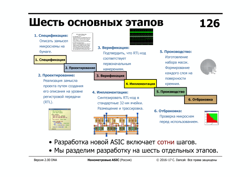
So far we have discussed the culmination of a microelectronic project - the manufacture of microcircuits in a factory. But how does such a project begin?
In the past 25 years, the design of the microcircuit is most often written in the language of the equipment description Verilog ([earlier] in Europe and among the military - VHDL), after which a special program (logic synthesis) turns the design into a graph of wires and logical primitives, another program (static timing analysis) tells the designer whether it fits into the speed budget, and the third program (place-and-route) lays out this design on the site of the chip.
When the design goes through all the stages: coding on a veril, debugging, verification, synthesis, static timing analysis, floorplanning, place-n-route, parasitics extraction, etc. - it turns out a file called GDSII, which is sent to the factory, and the factory bakes chips. The most famous factories of this type are owned by Taiwan Semiconductor Manufacturing Company or TSMC.
From a post on Habrahabr How to start developing iron using FPGAs - step by step instructions :
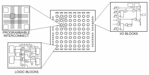
In the simplest version, an FPGA consists of a matrix of homogeneous cells, each of which can be changed into function using multiplexers connected to the bits of the configuration memory. One cell can become an AND gate with four inputs and one output, another - a single-bit register, etc. We load a sequence of bits from the memory into the configuration memory - and the given electronic circuit is formed in the FPGA, which can be a processor, display controller, etc.
FPGAs / FPGAs are not processors; by “programming” FPGAs (filling the configuration memory of FPGAs) you create an electronic circuit (hardware), while when programming a processor (fixed hardware) you slip a chain of sequential program instructions written into it (software).
Only registered users can participate in the survey. Please come in.
What to write about in the sequels?
- 59.5% about Cray and Illiac 28 supercomputers
- 53.1% about HP, DEC and Data General mini-computers 25
- 44.6% about the first microprocessors and microcomputers 21
- 61.7% about RISC workstations and Lisp machines 29
- 23.4% about game consoles and robots 11
- 2.1% other (explain in the comments) 1
- 8.5% why is this all? I am interested in quantum computers and singularity! 4