A Practical Implementation of the Switching Generator Using Verilog HDL
Abstract
Linear feedback shift registers are an excellent tool for implementing a pseudo random bit generator in hardware; they inhibit a simple and efficient electronic structure. Further, they are capable of producing output sequences with large periods and good statistical properties. However, standard LFSRs are not cryptographically secure, since the output sequence can be uniquely predicted given a small number of key stream bits using Berlekamp-Massey algorithm. Several methods have been proposed to destroy the linearity inherent in LFSR design. These methods include nonlinear combination generators, nonlinear filter generators, and clock controlled generators. Nevertheless, they remain vulnerable to many attacks such as side channel attacks and algebraic attacks. In 2015, a new clocked controlled generator, called the switching generator, was proposed. This new generator has been proven to be resistant to algebraic attacks and side channel attacks, while preserving efficiency and security requirements. In this project, we present a design of the switching generator using Verilog HDL.
Introduction and Historical Background
The history of pseudo random number generation in hardware is heavily linked to the development of stream ciphers. Stream ciphers are ciphers that encrypt plain text characters individually (usually bit by bit), in contrast to block ciphers, which encrypt plain text in large block (64 bits or more). Many stream cipher architectures require a key stream generator, which is a pseudo random bit generator whose seed is the encryption key. For each plain text bit, the corresponding cipher text bit is calculated as some revertible function (usually xor gate) of the plain text bit and the corresponding key stream bit. Therefore, designing safe and efficient key stream generators is essential for stream cipher operation.
One useful tool for building key stream generators is linear feedback shift registers. They can be contsructed easily using elementary electronic components, and can be programmed simply on programmable logic devices. Also, due to their simple structure, LFSRs can be modeled and analyzed mathematically, which has lead to a vast body of knowledge and results regarding them. The output sequence of a correctly constructed LFSR has exponential length and good statisitical properties such as large linear complexity.
Despite the good statistical properties of the LFSR, it cannot be used as a key stream generator in its strandard form due to its linear nature. If an attacker managed to know
- Using multiple LFSRs and a non-linear combining function of their outputs (non-linear combination generators).
- Generating the output sequence as some non-linear function of the LFSR state (non-linear filter generators).
- Irregular clocking of LFSRs (clock-controlled generators).
Still, all of these designs remained vulnerable to attacks such as algebraic and side channel attacks. After the year 2000, this was no longer a critical issue, as block cipher Rijndael was proposed and elected as the Advanced Encryption Standard (AES). AES was capable of operating in stream cipher mode and meet all industrial standards for a stream cipher. Further, with the rise of computational powers, AES could be deployed on various platforms. This has lead to a considerable decrease in stream cipher applications.
Adi Shamir presented an invited lecture in State of the Art in Stream Ciphers 2004 and Asiacrypt 2004 titled «Stream Ciphers: Dead or Alive?». In his presentation, he suggested that stream ciphers can survive in the following applications:
- Software-oriented applications with exceptionally high speeds (e.g. routers).
- Hardware-oriented applications with exceptionally small footprint (e.g. smart cards).
One of the latest proposals for key stream generators is the switching generator. It is claimed to be resistant to algebraic and side channel attacks, all while preserving efficiency and operating speeds.
In this project, we shall present a design of the switching generator in hardware, using Verilog HDL. First, we present the two common forms of LFSRs, Fibonacci LFSRs and Galois LFSRs. Next, we present a mathematical presentation of LFSRs. We will then present the switching generator as introduced by. Finally, we present our Verilog design of the switching generator.
Linear Feedback Shift Registers
Linear feedback shift registers are circuits consisting of a linear list of registers (also called delay elements) and a predefined set of connection among them. A global (single) clock signal controls the data flow inside the LFSR. The two most commonly used types of LFSRs are Fibonacci LFSRs and Galois LFSRs; deferring only in the form of connections. As we shall see later in the mathematical model section, there are many similarities between Fibonacci and Galois architectures, preferring one over the other is application specific.
Through out this article, we assume a hypothetical global time counter starting at
Registers
A register is a logic element capable of storing one bit of data, called the state. It has two input lines: a one bit data line and a clock signal line. It has a one-bit output that is always equal to the internal state. On every positive edge of the clock input, the data input is assigned to the state, otherwise the state remains unchanged. Let us denote the state of a register
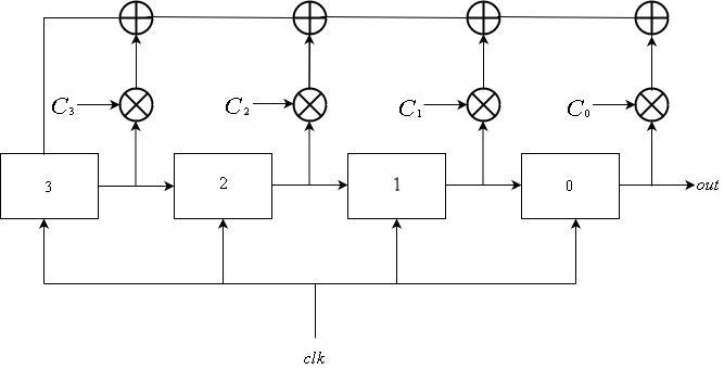
Fibonacci LFSRs
A Fibonacci LFSR consists of
The output sequence is obtained from register

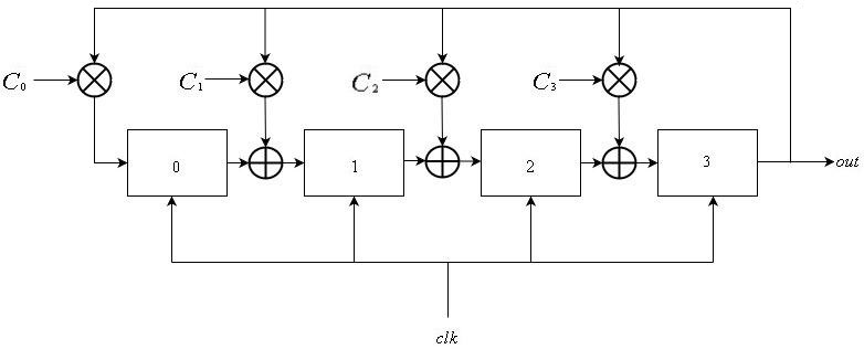
Galois LFSRs
Galois LFSRs also consist of a linear list of
In a manner similar to that of Fibonacci LFSRs, the output sequence is defined as

Comparison Between Fibonacci and Galois Designs
There is a direct correspondence between Fibonacci and Galois LFSRs in the mathematical sense, as we shall see in the next section. However, there are two notable advantages of using Galois' design:
- In software implementation, it does not require an
bit parity check, which adds a logarithmic factor of complexity.
- In hardware implementation, it only requires two-input xor gates, whose propagation delay is considerable less than that of the multi-input xor gates used in Fibonacci's design.
In our project, we consider the matrix formulation of the LFSR, so both architectures are interchangeable.
Mathematical Model of LFSRs
In the following sections, unless stated otherwise, we assume that all computation in done under Galois field
Consider the states of all
Consider the following linear transformation:
Given that
In this case, we have
Multiplying the state vector of some LFSR by a matrix (of Fiboancci or Galois types) is known as clocking or updating the LFSR.
The Switching Generator
The Switching Generator is a clock-controlled generator proposed in 2015. It is proven to have resistance to algebraic and side channel attacks. In this section, we shall present the design of the switching generator, as specified by the its inventors.
Basic Structure
The switching generator consists of two LFSRs: a control LFSR
The output of the switching generator is the output of LFSR
Integers
The Seed
Recall that an LFSR can iterate through at most
The seed for the switching generator is
Verilog Design
In this section, we shall introduce our design of the switching generator using Verilog HDL. We will present every module design in a bottom up fashion. At the very end, we introduce the switching generator module.
In our design, we tried to keep synchronous components to a minimum. The only clock controlled components are the LFSRs
Matrix and vector operations can be implemented in a number of different methods, varying in consumption of logic units, memory units and procedural complexity. In our design, we eliminate the need for procedural blocks, and use logic elements to a maximum.
All matrices in the following modules are indexed starting at
Also note that all modules have parameterized sizes; this is for debugging purposes. In an actual implementation, all sizes are fixed.
Multiplexer
This is a module implementing a 2 to 1
Multiplexer Module
Vector Transformation
This module implements a linear transformation on a vector. It accepts as input an
Each bit in the output vector is the result of an
Exactly
Vector Transformation Module
Identity
This module accepts no input. Its
Identity Matrix Module
Transpose
This module accepts an
Matrix Transpose Module
Matrix Multiplication
This is a module implementing matrix-matrix multiplication. It accepts two
This module contains an instance of the matrix transpose module. This makes it possible to assign consecutive indices to columns in the second input matrix. Each entry in the output matrix is then assigned to the output of an
Exactly
Matrix Multiplication Module
Matrix Exponentiation
This module raises a matrix to an integer power. It accepts as input an
Matrix Exponentiation Module
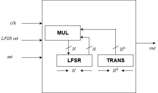
Control Unit
This module implements the
It includes a static
After each positive edge of the clock signal, the state is updated according to the transformation matrix using a matrix-vector multiplication module. The state reset is assigned to the internal state after each positive edge of the reset signal.

Control Unit Module
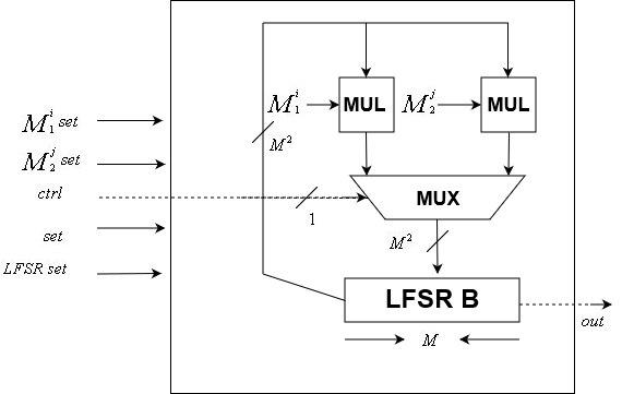
Data Unit
The
The module includes two
Note that since the seed can be changed, then the transformation matrices can also be changed, unlike the control unit whose transformation matrix if fixed.

\Data Unit
The Switching Generator
This is the main module of our design. It is parameterized by integers
The input to this module is a clock signal, a
This module includes two
Two matrix exponentiation modules instances are used to calculate the input matrices for the data unit, where their input are the fixed transformation matrices and integers
The Switching Generator Module
Conclusions and Recommendations
In this project, we have presented a design of the switching generator using Verilog HDL. This design is focused entirely on hardware, and eliminates the use of procedural blocks. Such an approach allows for maximum performance at the cost of logic and memory elements. For some applications with logic and memory elements constraints, it might be beneficial to sacrifice performance and increase the use of procedural blocks to reduce electronic elements usage.
One drawback of the project it that it lays the responsibility of choosing good switching indices on the user. One possible advancement is adding a hardware component to check the validity of the used switching index. This requires a hardware implementation of complex algorithms such as finding the characteristics polynomial of a given matrix and checking it for primitivity.
A possible advancement is adding a true random number generator to check random switching indices, and outputting a valid pair once it is found. It can be proven that this process halts after a short time with high probability.
References
- Katz, Jonathan, et al. Handbook of applied cryptography. CRC press, 1996.
- Choi, Jun, et al. «The switching generator: New clock-controlled generator with resistance against the algebraic and side channel attacks.» Entropy 17.6 (2015): 3692-3709.
- Shamir, Adi. «Stream ciphers: dead or alive?.» ASIACRYPT. 2004.
- LFSRs for the Uninitiated
