Power converter control module: development and assembly
It's no secret that complex modern converters, for example, online UPS, are running DSP / MK or ASIC. The main suppliers of DSP for power electronics are two companies - Texas Instruments and Infineon, but today we are talking about STMicroelectronics products - the STM32F334 series. This line MK is designed to control the drive and build power converters: PFC, inverters, switching power supplies, UPS and others.
Of course, the F334 series cannot withstand the “power” of such popular solutions as TMS320F28335 and other things, but it has one important advantage — cost. The older STM32F334R8T6 stone costs $ 5, has the necessary peripheral set (HRPWM, ADC, comparators) and performance for building powerful enough converters (tens of kilowatts) with good reliability and fault tolerance.
For the developer of electronics, the ecosystem around the DSP / MK with which he works is important: documentation, debugging tools, code samples and hardware. TI has it all, yes - it's expensive, yes - it's hard to buy, but it is and that is why in most modern solutions in the field of electric drive and power engineering there are TMS320. For some reason, ST company overlooked the F334 series, although there is good quality documentation as any STM32 is available, but there are no examples of hardware with a full code and debug boards (the F3348-Disco toy does not count). Well, we will correct this deficiency.
In his last articleI talked about my project “developer kit” and even demonstrated one of the components - the power module. Today I will talk about the 2nd (there will be 3 in total) module, which allows you to implement any converter topology and at the same time is several times cheaper than competitors. The project is of course open and all the sources can be viewed at the end of this article.
I am far from being the first to think about using a kind of universal module on the basis of which you can build different converters with different topology options. This approach allows you to have one board for all occasions and the main thing is to reduce the amount of code, because the module is the same, once set up and forgotten.
Let's now look at a couple of examples of how this idea has already been implemented by other people / companies. I will give just two examples:
And so, what did you want to do in the end ... A module that can be used both as a debugging tool and as a component in a small series. From here are a number of requirements that I have got:
The result was the following structural scheme:
It should be noted right away that I also managed to significantly reduce the cost of the module. I ordered components on 5 boards, where components bypassed at ~ $ 70, that is, $ 14 / module. Here the true trick is the cost of all the components, but without the PCB. The arithmetic is simple: ordering 5 boards in 4 layers costs $ 80-100, that is, another $ 14-20 for each module, don't you agree humanely? With the number of 100 pieces, the cost of the board is already $ 1.5 / piece, so in the foreseeable future I plan to order 100-200 boards (see how cheaper it will be) and those who want will have the opportunity to buy boards at times cheaper than $ 14. Those who need 20-30 boards or $ 100 do not bother you, they can already order them themselves, the benefit of the gerbera will also be prepared.
There is nothing complicated and incomprehensible in the circuitry of the module, for a start I suggest you open a schematic diagram so that you understand what it is about and I will tell you how the structural diagram above has turned into a ready-made solution. Download the scheme here - PDF .
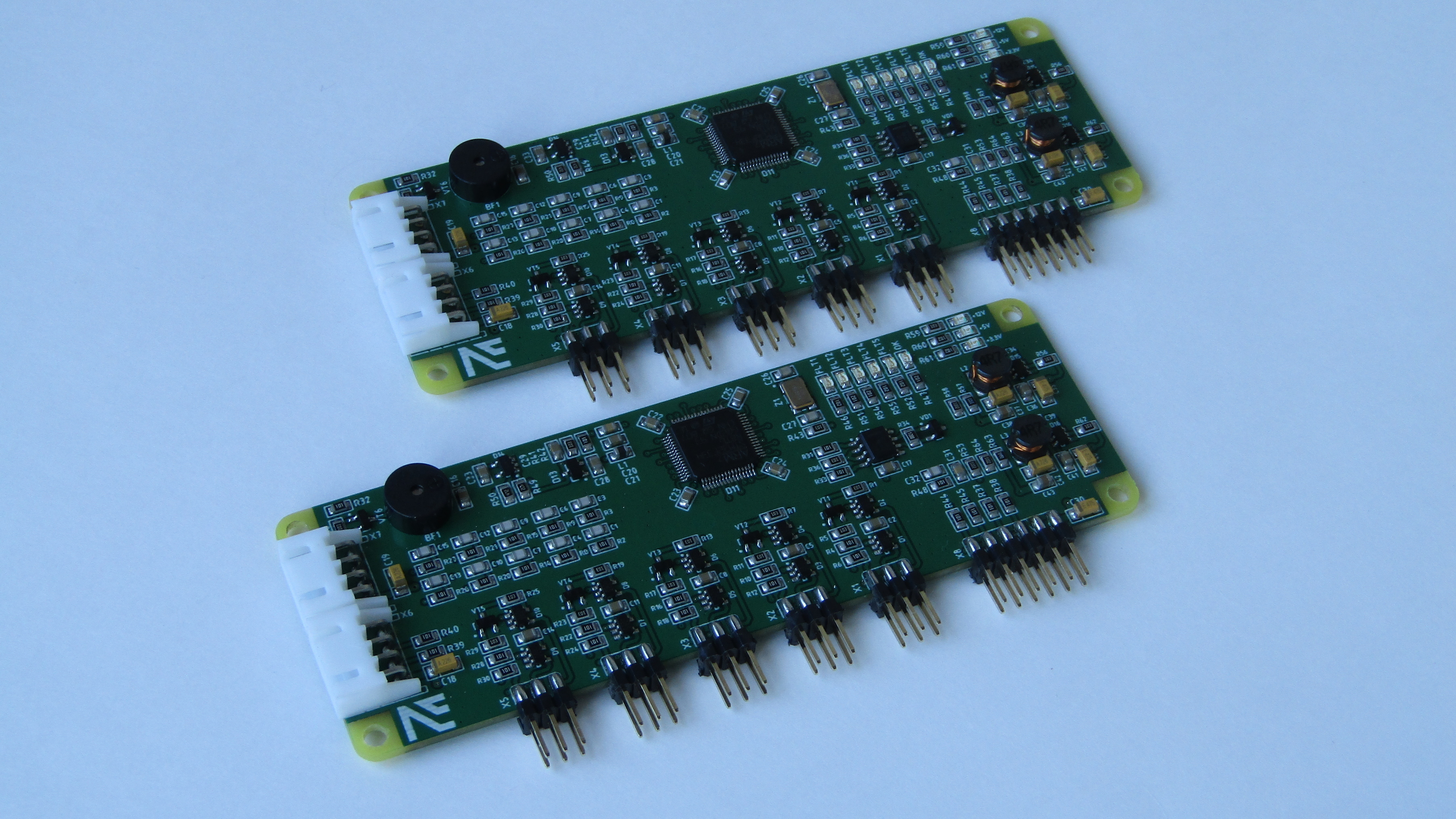
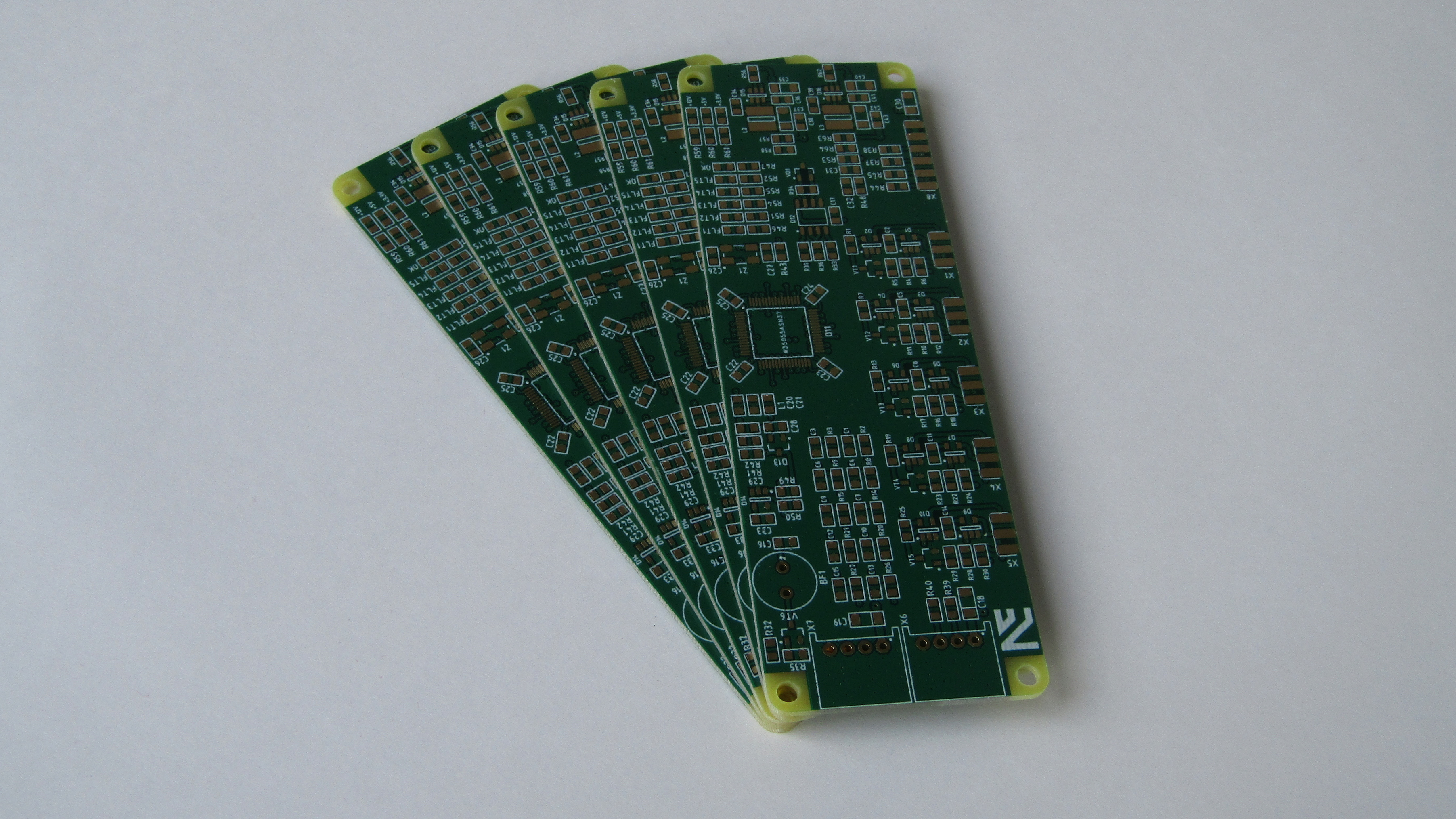
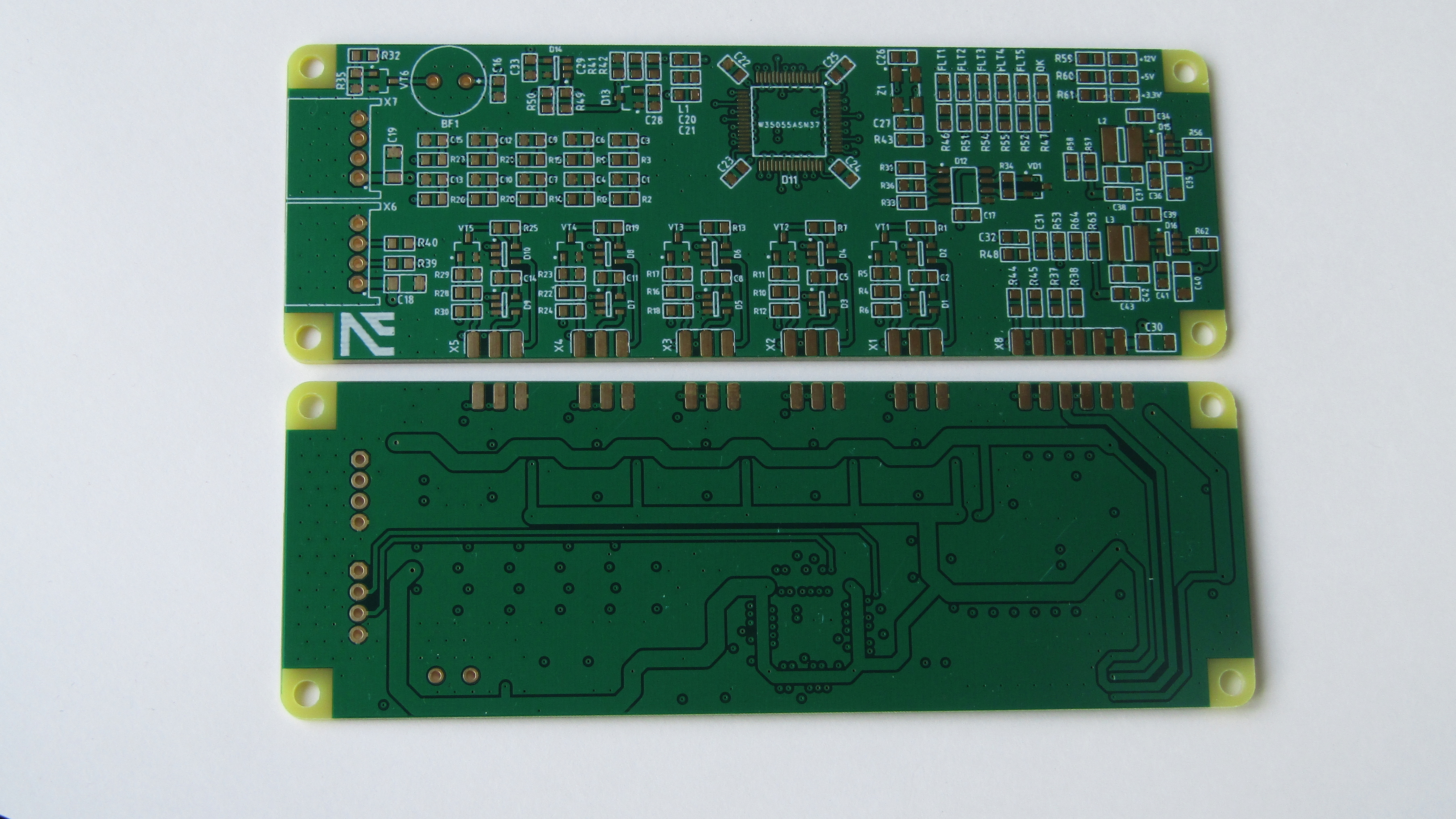
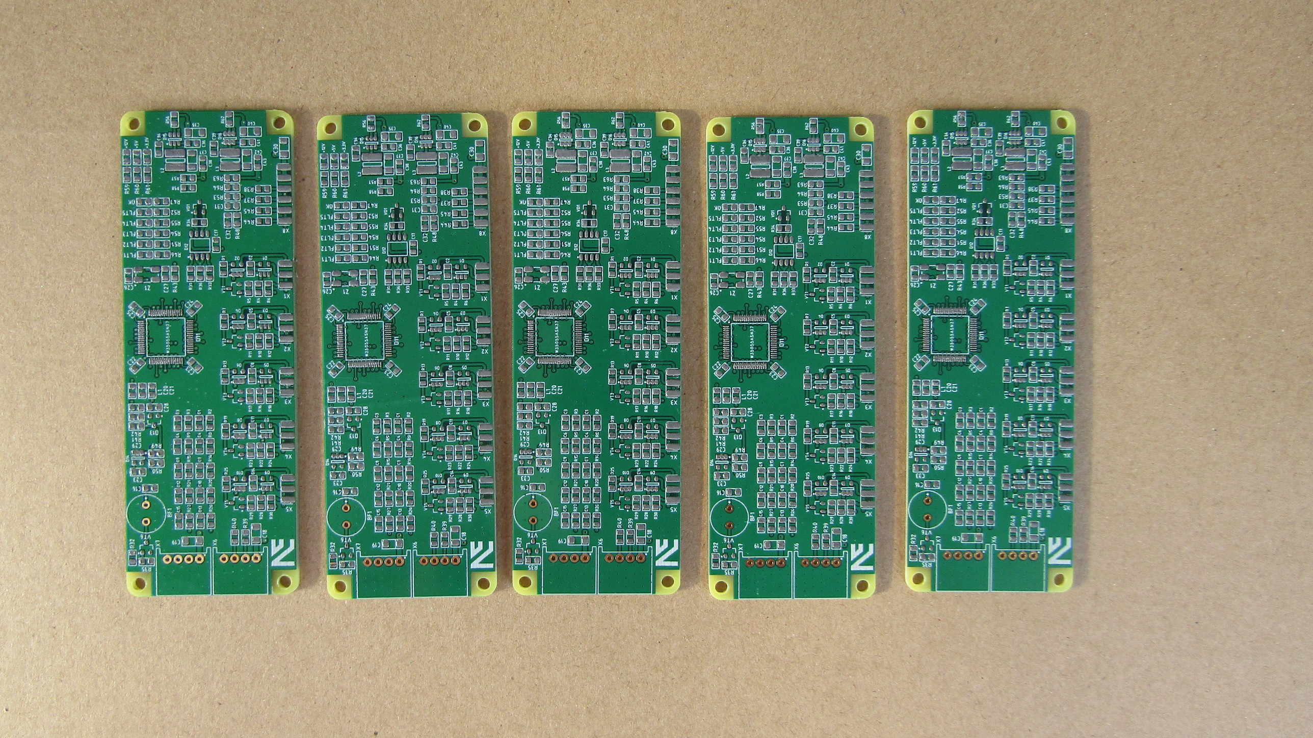
This circuit diagram eventually turned into a 4-layer PCB size 115x40 mm. In principle, you can dilute your version in 2 layers, but the dimensions will grow. It was important for me to get a width of no more than 40 mm, so that after installation in PBD connectors, the total height was 47-50 mm - in terms of electrolytic capacitors 35x50 mm. The board looks like this:
Unfortunately, when I ordered the boards, I indicated a green mask instead of a black mask - the main fiasco of this revision)) Whoever did not understand how the module is inserted, I suggest looking here:
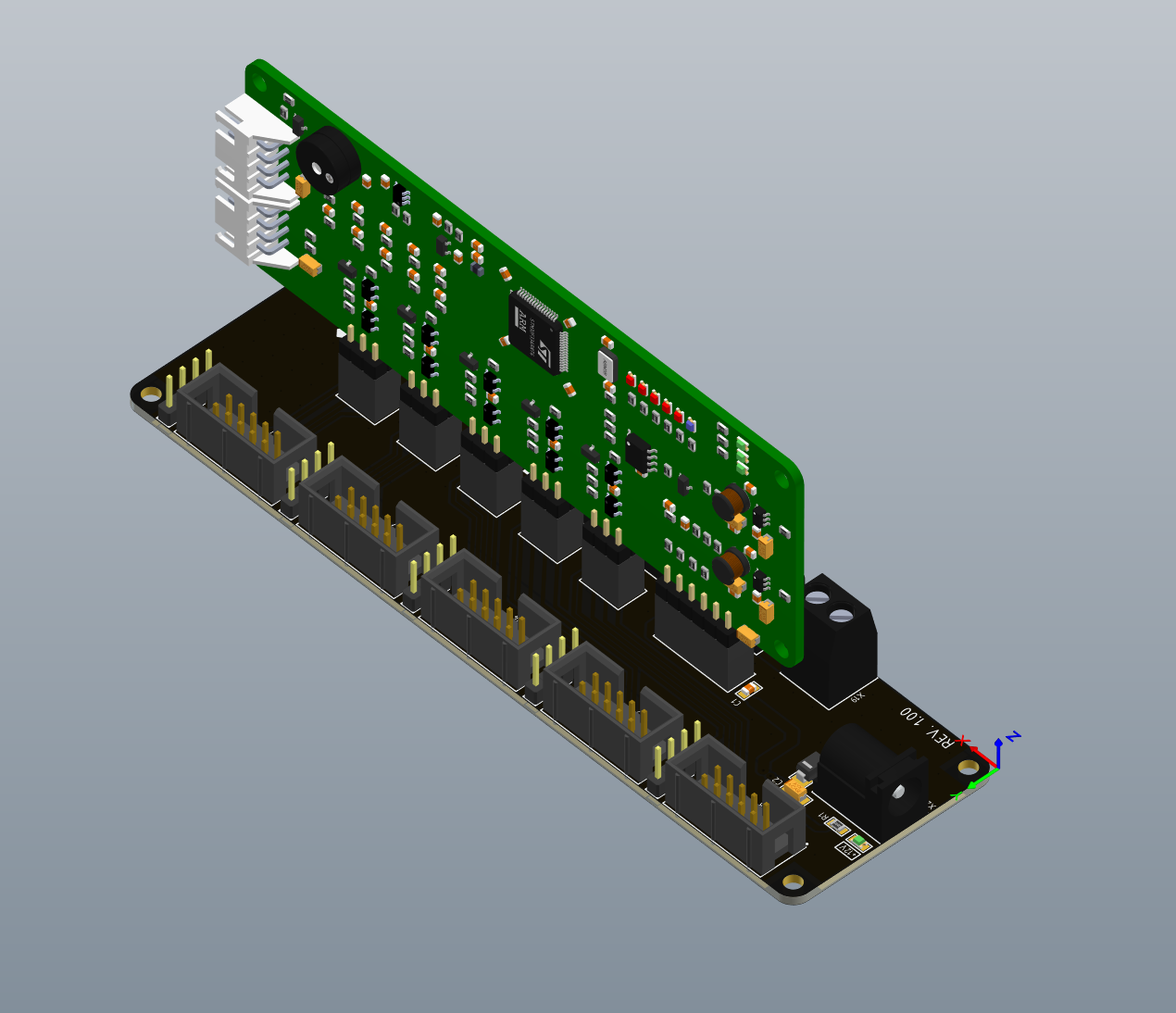

In the first picture you can also notice a certain board with a bunch of connectors and especially without components. This is something like a “motherboard” for more convenient prototyping. BH-10 connectors (IDC-10) distribute those same 5 control channels + to the terminal blocks the communication interfaces are output and the power connector is installed. All this allows not to collective farm a bunch of wires. “Motherboards” were ordered separately, so they will come later and after verification there will be available source codes.
As for the previous module, the PCBs were ordered from PCBway , the guys were provided with free cards and another stencil. The latter made my life much easier and saved time, 5 boards with 200+ components each were assembled in 1 hour. 2 weeks after the order, the couriers brought me such a charm: Yes, I did not change the mask on the order form, but apparently feeling this I wasgilded with a pen covered with immersion gold so that I would not be sad. For my task, this is not critical, but due to the excellent planarity of the contacts, the solder paste is applied evenly and the components do not lead to the sides, even if the thermal profile for the furnace is not very optimal.
The stencil was ordered with a frame made of aluminum, because I have a stencil printer, and without a frame I can’t fix it there. If you don’t have a printer, order without a frame: you will be able to apply paste (you spend a few minutes longer) and still save money, because stencil without frame weighs about 400 grams, and with a frame of 1.8 kg. Because of this weight, you immediately get on delivery by courier, because mail does not carry more than 2 kg, only EMS and you will have to pay $ 30-40 more, so please note. The stencil itself looks like this:
Now you need to install the board in the printer and apply the paste. Here are a couple of tips. Firstly, if you take the paste for aliexpress, then only 500 g cans, it is of the best quality (apparently it is stored correctly). Second, store the pasta in the fridge. Third, after using the stencil, be sure to wash it off the paste, a regular sponge and a droplet of detergent (the best is best) work wonders, then dry the stencil and, after drying, wrap in cling film if you do not use it for more than a week. Apply the paste to the board:
After applying we get the following blank:
At this stage, I will be safe: I will remove the paste for the LQFP-64 case under the STM32F334R8T6 microcontroller. The fact is that I could nakosyachit somewhere in the power system and there is a chance that + 12V will fall on the MC and burn it, but I would not want to destroy the stones at $ 5. Therefore, I solder everything at this stage except the microcontroller, the connectors and the buzzer. I will install them already manually after checking the voltages of + 3.3V and + 5V. Now the most boring stage is to install the components, but I’m planning to buy a pick place machine, and I’ll just drink coffee)) The components are installed and now send them to the oven: Now it remains to check the voltage levels at the output dc / dc and if everything is OK , then we solder the remaining components with a soldering iron / hairdryer, go and launder the board from the flux residues and get the following result:


We connect the programmer, for example, the Chinese whistle st-link, but I strongly advise you to purchase a firm st-link v.2-ISOL with galvanic isolation. It's all like admins with backups: "Some have already burned a laptop and started using insulators, others have not yet started using insulators . " If the price tag on the native st-link frightens you, then there is an option to purchase an insulator module on Ali along with a Chinese whistle, they are usually implemented on ADuM-ah. In order not to suffer with a pinout when connecting a debugger, I made a cord for connecting these modules, now I’ll not let the connection error exactly:

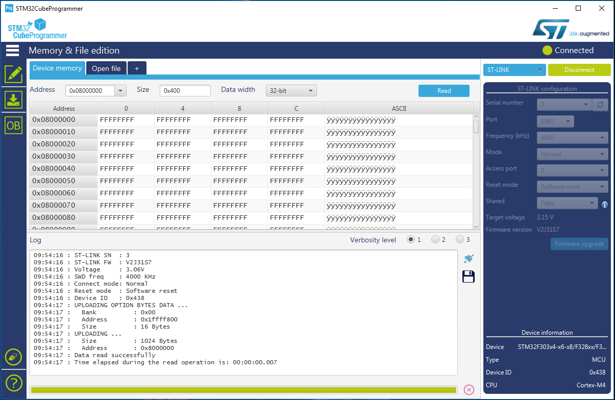
It remains to check if the module is ready for operation, if the MK is read, so that we can calmly start writing code. To do this, you can install the utility STM32CubeProgrammer. Open it, you should determine your debugger, if you saw its id in the upper right corner, then click Connect and if everything is mounted correctly, you will see the microcontroller id, the core, the MK series itself (I have F334):
That's all! The module is ready for operation and development of various converters.
Now there are 2 modules for development, this is enough to build a converter. Of course there will be a 3rd module, but without HMI you can live, and those who are interested can purchase nextion in their own pocket. In the next article, it will be possible to assemble a full-fledged converter, to realize the P and PI regulators which we so zealously asked in the comments. For obvious results, the following articles will be on specific topologies: their analysis, calculations, prototyping, code, and most likely will begin with the buck and boost topologies, as the simplest and most common.
I would also like to thank the guys from PCBway who help with boards of any complexity of excellent quality. Thanks to them, the project is moving quite actively and in a couple of months I managed to do something that was too lazy to implement the previous couple of years.

I hope the article was interesting to you, if you have some questions about the topology of the buck in advance, then you can voice them in the comments or the LAN, and I will try to answer them when writing the next article and thereby make the material more useful.
Of course, the F334 series cannot withstand the “power” of such popular solutions as TMS320F28335 and other things, but it has one important advantage — cost. The older STM32F334R8T6 stone costs $ 5, has the necessary peripheral set (HRPWM, ADC, comparators) and performance for building powerful enough converters (tens of kilowatts) with good reliability and fault tolerance.
For the developer of electronics, the ecosystem around the DSP / MK with which he works is important: documentation, debugging tools, code samples and hardware. TI has it all, yes - it's expensive, yes - it's hard to buy, but it is and that is why in most modern solutions in the field of electric drive and power engineering there are TMS320. For some reason, ST company overlooked the F334 series, although there is good quality documentation as any STM32 is available, but there are no examples of hardware with a full code and debug boards (the F3348-Disco toy does not count). Well, we will correct this deficiency.
In his last articleI talked about my project “developer kit” and even demonstrated one of the components - the power module. Today I will talk about the 2nd (there will be 3 in total) module, which allows you to implement any converter topology and at the same time is several times cheaper than competitors. The project is of course open and all the sources can be viewed at the end of this article.
Idea
I am far from being the first to think about using a kind of universal module on the basis of which you can build different converters with different topology options. This approach allows you to have one board for all occasions and the main thing is to reduce the amount of code, because the module is the same, once set up and forgotten.
Let's now look at a couple of examples of how this idea has already been implemented by other people / companies. I will give just two examples:
- TMS320F28379D Control card - cost $ 160. The ecosystem is excellent, there are debugging complexes for it, but the price is ... Is it small if you work in a well-to-do R & D center, and if you decide to build UPS for yourself or work for the company easier? And it seems to me that everyone will be sorry for the $ 160 module;
- VectorCARD К1921ВК01Т is an excellent solution, and even on the domestic stone,
people in scientific research institutes and military industrial complex are jubilant, there is a debugging complex in the form of a frequency counter, an analogue (pin-to-pin) with a module from ti, but the price is 19,000 rubles. For the harsh domestic industrial and military industrial complex is cheap, and the rest is not very.
And so, what did you want to do in the end ... A module that can be used both as a debugging tool and as a component in a small series. From here are a number of requirements that I have got:
- Availability of HRPWM and fast ADC
- RS-485 on board
- UART with output for a display connector (compatible with Nextion)
- Implementing hardware protection on logic
- 12V power supply to use one AC / DC to 12V module for both the “brain” and power drivers
- The cost is at least 3 times lower than the cost of the TMS320F28379D Control card, that is, $ 50 maximum
- Radiator temperature sensor input
- A couple of GPIO, for example, a relay pull
- Sync signal input and output so that multiple devices can be paralleled
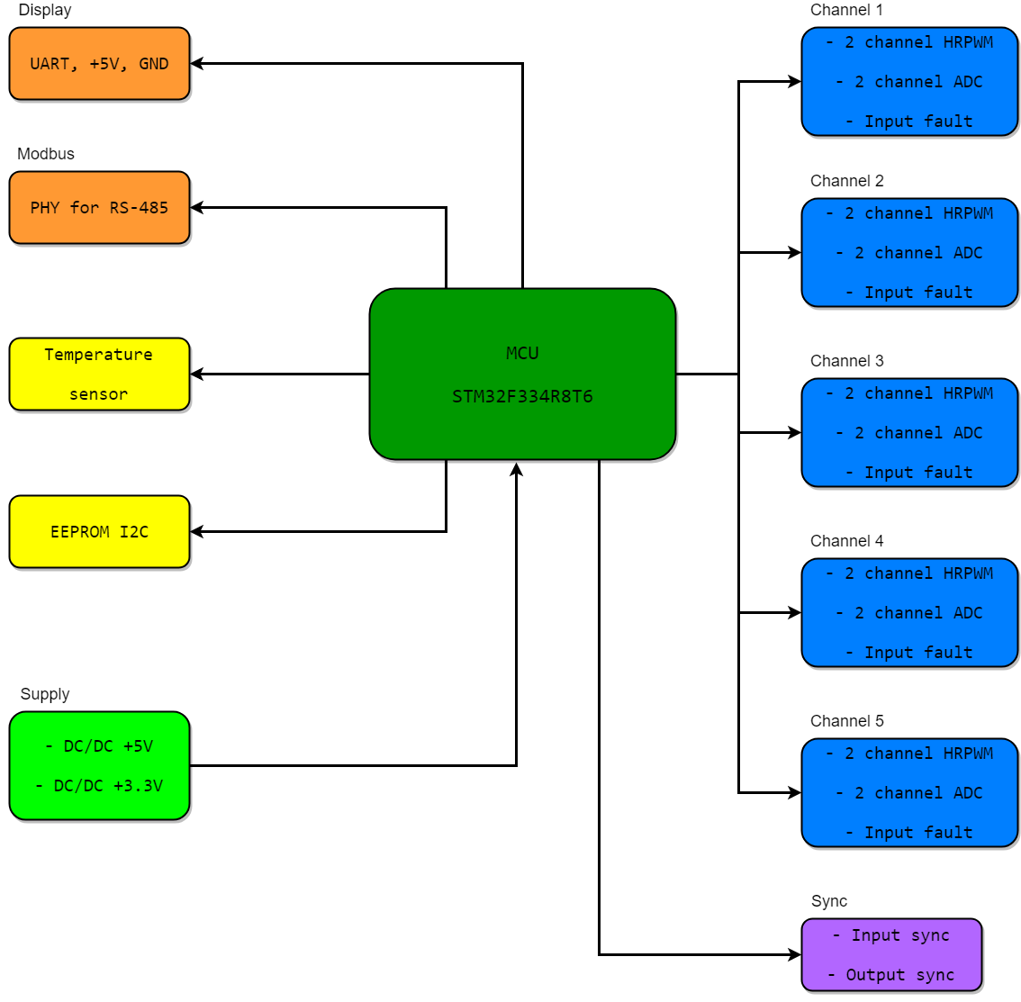
The result was the following structural scheme:
It should be noted right away that I also managed to significantly reduce the cost of the module. I ordered components on 5 boards, where components bypassed at ~ $ 70, that is, $ 14 / module. Here the true trick is the cost of all the components, but without the PCB. The arithmetic is simple: ordering 5 boards in 4 layers costs $ 80-100, that is, another $ 14-20 for each module, don't you agree humanely? With the number of 100 pieces, the cost of the board is already $ 1.5 / piece, so in the foreseeable future I plan to order 100-200 boards (see how cheaper it will be) and those who want will have the opportunity to buy boards at times cheaper than $ 14. Those who need 20-30 boards or $ 100 do not bother you, they can already order them themselves, the benefit of the gerbera will also be prepared.
Development
There is nothing complicated and incomprehensible in the circuitry of the module, for a start I suggest you open a schematic diagram so that you understand what it is about and I will tell you how the structural diagram above has turned into a ready-made solution. Download the scheme here - PDF .
- The module has 1 “main connector”, where 12 pins carry 12V power, a couple of GPIO, an additional UART (suddenly you want to screw the ESP), RS-485 and input / output to synchronize devices;
- There are 5 channels, they are all exactly the same. Each channel has a complementary pair of High result PWM (HRPWM), which allows you to control the half-bridge. There are also 2 ADC channels for the implementation of current and voltage feedback and the cherry on the cake - fault input. For example, you have a short circuit in the power section, the comparator detected the excess current and issued a log. 1 as a sign of an accident, so feed “1” at this input interrupts the operation of the device
- The error signal from the fault input goes to 2 places: to the BKIN input of the microcontroller and through the inverter to the input of the AND gate. The BKIN input is also a hardware protection and turns off the PWM generation even if the MK is frozen, but I wanted to play it safe and add more logic so that it exactly broke the signal;
- On the module, the SWD interface is brought into a separate CWF-4 connector for easy debugging, and the UART and power supply for connecting the display or communicating with other modules are brought to the second connector. Nextion displays are now popular, so the connector for them is designed and I also make my HMI panel with a similar communication method (UART, + 5D, GND);
- The board contains a PHY for the RS485 interface with a terminating resistor and ESD protection. The choice of this interface fell because it is anywhere, because it is an industry standard. For example, you will want to combine your voltage inverter with a diesel and it will be convenient to send / receive commands. Yes, and in any PLC there is also RS485;
- I also installed a small non-volatile memory for storing settings or something else useful.
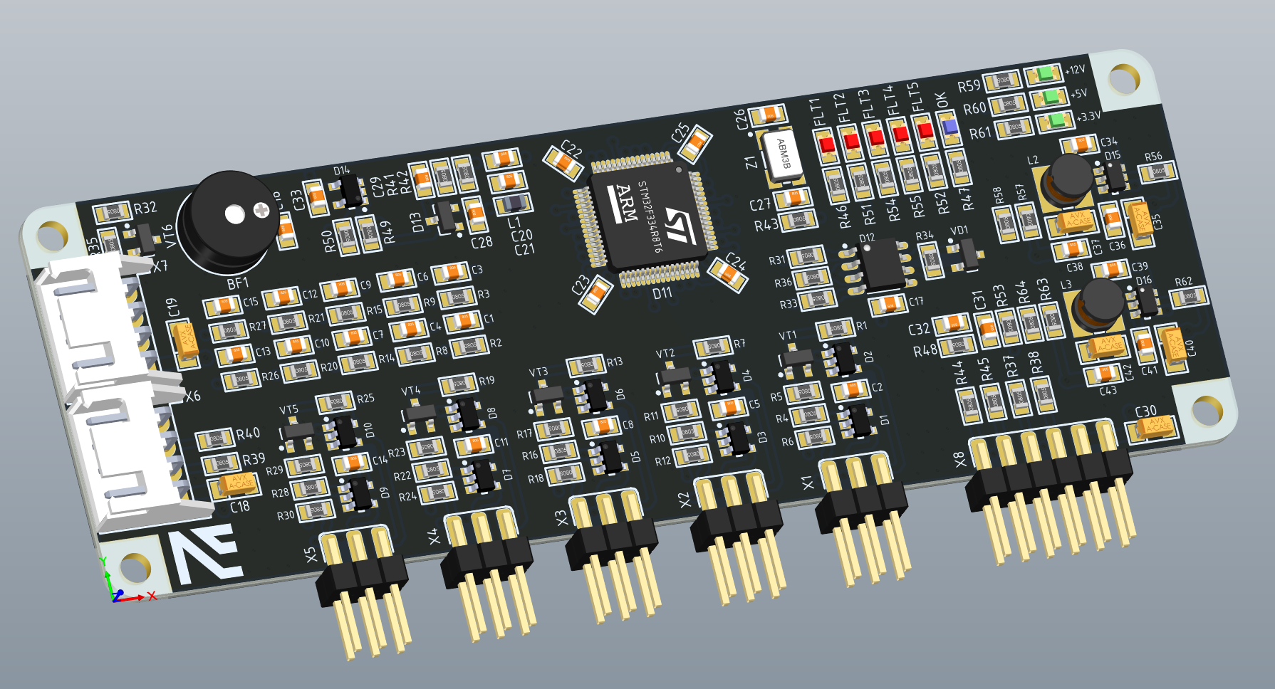
This circuit diagram eventually turned into a 4-layer PCB size 115x40 mm. In principle, you can dilute your version in 2 layers, but the dimensions will grow. It was important for me to get a width of no more than 40 mm, so that after installation in PBD connectors, the total height was 47-50 mm - in terms of electrolytic capacitors 35x50 mm. The board looks like this:
Unfortunately, when I ordered the boards, I indicated a green mask instead of a black mask - the main fiasco of this revision)) Whoever did not understand how the module is inserted, I suggest looking here:
In the first picture you can also notice a certain board with a bunch of connectors and especially without components. This is something like a “motherboard” for more convenient prototyping. BH-10 connectors (IDC-10) distribute those same 5 control channels + to the terminal blocks the communication interfaces are output and the power connector is installed. All this allows not to collective farm a bunch of wires. “Motherboards” were ordered separately, so they will come later and after verification there will be available source codes.
Assembly
As for the previous module, the PCBs were ordered from PCBway , the guys were provided with free cards and another stencil. The latter made my life much easier and saved time, 5 boards with 200+ components each were assembled in 1 hour. 2 weeks after the order, the couriers brought me such a charm: Yes, I did not change the mask on the order form, but apparently feeling this I was
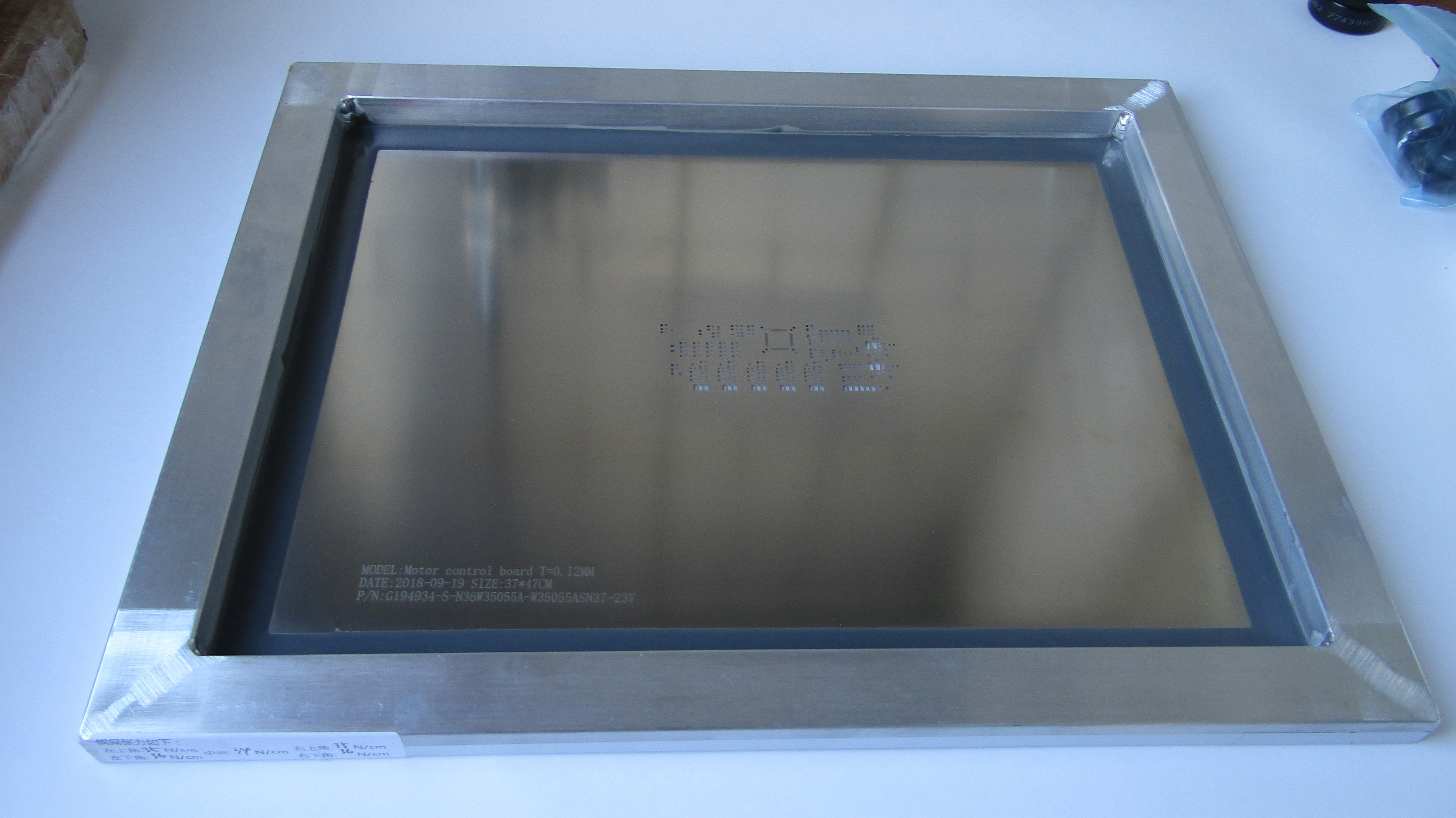
The stencil was ordered with a frame made of aluminum, because I have a stencil printer, and without a frame I can’t fix it there. If you don’t have a printer, order without a frame: you will be able to apply paste (you spend a few minutes longer) and still save money, because stencil without frame weighs about 400 grams, and with a frame of 1.8 kg. Because of this weight, you immediately get on delivery by courier, because mail does not carry more than 2 kg, only EMS and you will have to pay $ 30-40 more, so please note. The stencil itself looks like this:
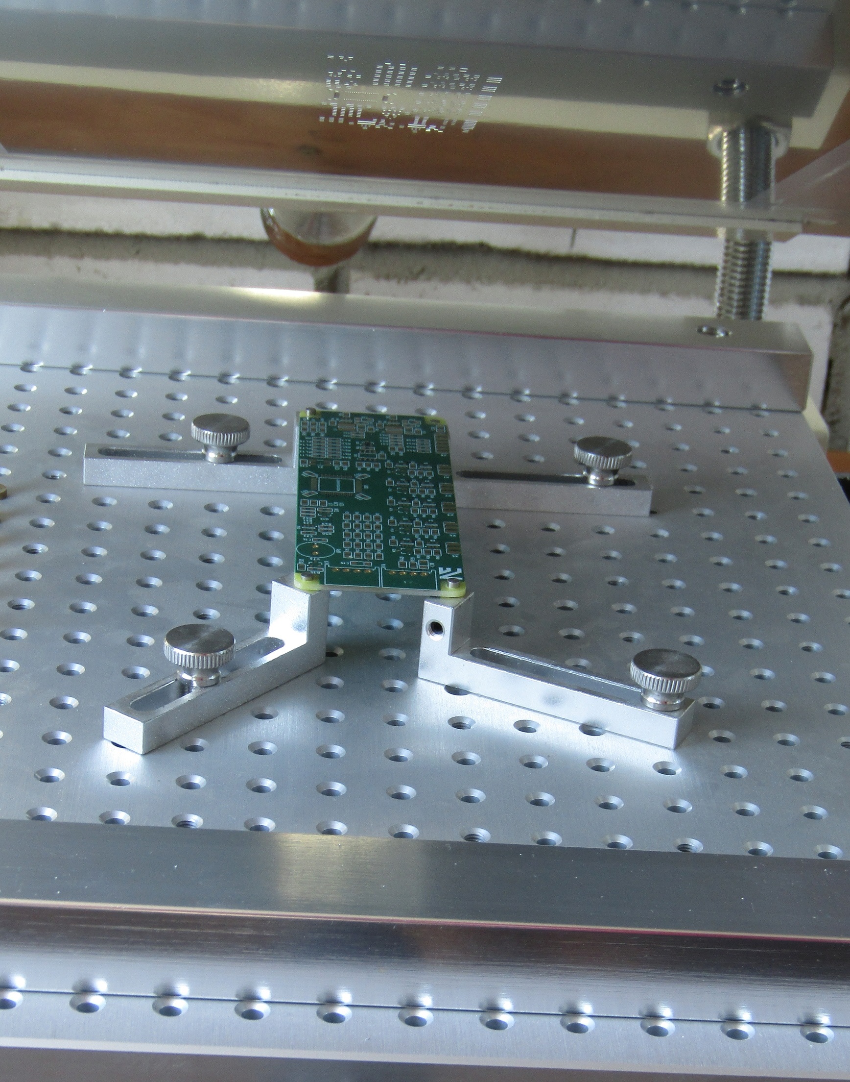
Now you need to install the board in the printer and apply the paste. Here are a couple of tips. Firstly, if you take the paste for aliexpress, then only 500 g cans, it is of the best quality (apparently it is stored correctly). Second, store the pasta in the fridge. Third, after using the stencil, be sure to wash it off the paste, a regular sponge and a droplet of detergent (the best is best) work wonders, then dry the stencil and, after drying, wrap in cling film if you do not use it for more than a week. Apply the paste to the board:
After applying we get the following blank:
At this stage, I will be safe: I will remove the paste for the LQFP-64 case under the STM32F334R8T6 microcontroller. The fact is that I could nakosyachit somewhere in the power system and there is a chance that + 12V will fall on the MC and burn it, but I would not want to destroy the stones at $ 5. Therefore, I solder everything at this stage except the microcontroller, the connectors and the buzzer. I will install them already manually after checking the voltages of + 3.3V and + 5V. Now the most boring stage is to install the components, but I’m planning to buy a pick place machine, and I’ll just drink coffee)) The components are installed and now send them to the oven: Now it remains to check the voltage levels at the output dc / dc and if everything is OK , then we solder the remaining components with a soldering iron / hairdryer, go and launder the board from the flux residues and get the following result:
We connect the programmer, for example, the Chinese whistle st-link, but I strongly advise you to purchase a firm st-link v.2-ISOL with galvanic isolation. It's all like admins with backups: "Some have already burned a laptop and started using insulators, others have not yet started using insulators . " If the price tag on the native st-link frightens you, then there is an option to purchase an insulator module on Ali along with a Chinese whistle, they are usually implemented on ADuM-ah. In order not to suffer with a pinout when connecting a debugger, I made a cord for connecting these modules, now I’ll not let the connection error exactly:
It remains to check if the module is ready for operation, if the MK is read, so that we can calmly start writing code. To do this, you can install the utility STM32CubeProgrammer. Open it, you should determine your debugger, if you saw its id in the upper right corner, then click Connect and if everything is mounted correctly, you will see the microcontroller id, the core, the MK series itself (I have F334):
That's all! The module is ready for operation and development of various converters.
Sources
- Schematic diagram - PDF
- Component List (BOM) - Excel
- PCB Gerber Files - RAR
- Project with pinout for STM32CubeMX - IOC
Conclusion
Now there are 2 modules for development, this is enough to build a converter. Of course there will be a 3rd module, but without HMI you can live, and those who are interested can purchase nextion in their own pocket. In the next article, it will be possible to assemble a full-fledged converter, to realize the P and PI regulators which we so zealously asked in the comments. For obvious results, the following articles will be on specific topologies: their analysis, calculations, prototyping, code, and most likely will begin with the buck and boost topologies, as the simplest and most common.
I would also like to thank the guys from PCBway who help with boards of any complexity of excellent quality. Thanks to them, the project is moving quite actively and in a couple of months I managed to do something that was too lazy to implement the previous couple of years.
I hope the article was interesting to you, if you have some questions about the topology of the buck in advance, then you can voice them in the comments or the LAN, and I will try to answer them when writing the next article and thereby make the material more useful.