Multicrystal: from history to speculation about the future

MCM: multi-chip layout
Microelectronics is famous for a large number of original, strange and effective engineering solutions. One of them is a multi-chip layout, which is somehow found almost everywhere - from high-performance workstations to ultraportable laptops, from single-board computers for $ 10 to IBM mainframes.
This post tells the story of its use in relation to general-purpose processors. I
warn you in advance: I do not pretend to have absolute knowledge and academic character of presentation, I tell mostly about what I encountered, worked and held in my hands.
Traffic Warning! Under the cut a lot of pictures!
What is it?
MCM (Multi-chip module, multi-chip module) or MCP (Multi-chip package, multi-chip layout) - an engineering solution to break the functionality of the chip into several chips combined into one case. It differs from modules in that the microcircuits are usually “bare”, without a compound, and soldered directly to the board with crystals. It is used to increase the yield of suitable chips (reducing the size of an individual crystal), a compact connection of crystals made according to different technical processes and technologies.
So, let's start?
1995: When the cache does not fit into any gate
(aka Pentium Pro)
Cache - tricky thing, dimensional and fast. This is where a couple of problems arise: with an increase in the speed of its work, the throughput of its tire becomes a bottleneck, and it starts to get warm. We need to fix this somehow. The most logical way is to transfer L2 to the processor, where L1 has been grazing for a long time. But there is a problem, and not one: with an increase in the size of the crystal, the percentage of chip rejects increases, and almost exponentially. What to do? Of course, make the cache a separate chip, but closer to the main one. As a result, we can admire this brick:

The solution is good, but it has considerably complicated the construction.
1997: And now for an encore, though not the same
(aka Pentium II)
A large ceramic body is, of course, good, but expensive. Try to replay? Why not. The task is to make it cheaper, and that’s all. Transferring the cache back to the board is not an option - it would be a step back. And the width of the bus cache has also grown ... Can it combine everything with cooling into one module? So the Pentium II was born:
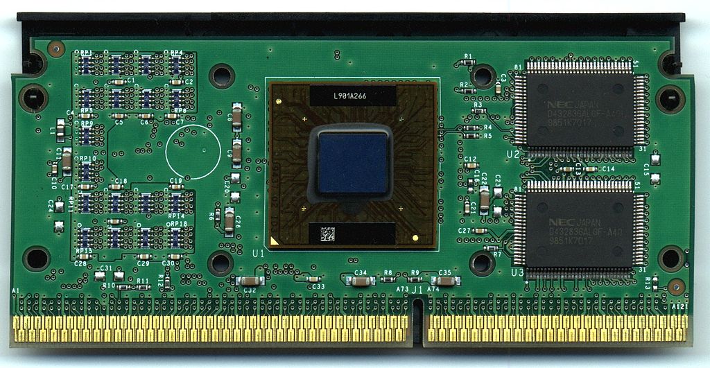
You can, of course, not consider this an MCM, but since I remembered it, it will be here.
(by the way, without this permanent and immortal old man, your humble servant would not have written this article - the PII-400 which has been working for me for a year as a gateway and WiFi router, having outlived many of its descendants)
2005: D means Double Bottom
(aka Pentium D)
When the plan “One core, but THINKING!” Started palpably at the seams, and the competitors, chuckling, were about to release dual-core processors on a single chip, they had to do something, and quickly. So this atavism appeared, by which they plugged a hole in the market, while the main forces were thrown onto the more promising Core architecture. Probably the main reason for using such a solution was precisely the reduction in development time — the size of the crystals was not so large that its doubling caused problems. Well, here's how it happened:

There were similar Xeon processors for the server segment, but I can say little about them.
2007: Why not?
(aka Core 2 Quad)
Since we mastered two-core crystals in 2006, why strain? We use the time-tested solution - stick two crystals in one case and there are no problems! There is nothing to talk about, the picture has not changed much: the
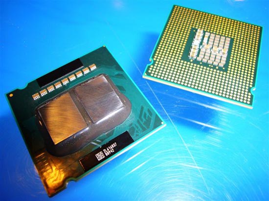
Xeon of that era was also such, except for the six-core model - there is one big crystal.
2010: Before the arrival of the sand
(aka first gen Core i3 / 5/7)
On dual core Core i processors of the first generation, they decided to run a 32 nm process, having done a rather amusing thing - they made an integrated video core and a memory controller on a time-tested 45 nm process, and a pair of cores with a cache was placed on a separate 32 nm chip. While their older quad-core cousins used the 45nm process! The size of the crystals is also funny:

(However, the video core for dual-core processors and now often larger than both cores together)
2011: One bulldozer is good, but two is better
(aka Opteron 6000)
The crystal is already so big, the technology of their release is adjusted, what are the problems? NUMA? But we are already doing these processors for servers, and multi-socket. If there are no problems, we collect two crystals under one cover:
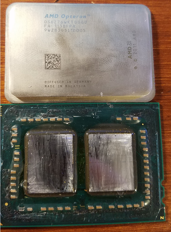
(Aha, and then people have fun - there is one processor, and NUMA nodes - two)
2013: Toffee but inedible
(aka eDRAM L4 GPU / CPU cache)
Since the generation of Haswell, processors equipped with integrated graphics Iris Pro / Iris Plus (and in the generation of Skylake - and those with the usual Iris) come in the same package with 64 / 128MB memory chip, working as L4 cache and seriously raising the performance of integrated graphics. And the chip is not small (although memory always takes up a lot of space):

2017: Year when Intel shit brix
(aka Ryzen Threadripper & EPYC)
AMD engineers played with Infinity Fabric, played ... And then - oops! Four crystals under one lid are connected with IF each with each (in the case of server EPYC) or a pair between each other (a Threadripper with two active crystals). All is well, only one problem is NUMA (as many as 4 nodes per processor!), But the problem is only for unsuitable software. So it came out very well:
2018: Double the amount - double the fun
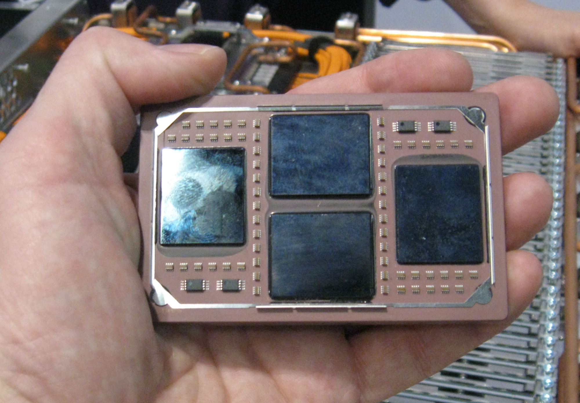
(aka Zen 2 & Cascade Lake AP)
So we got to current events. On November 5, Intel quickly announced the 48-core dual-chip processors (even the pictures didn’t have time to make photos), and on November 6, AMD showed new EPYCs at its Next Horizon event. A thousand words will replace the picture:
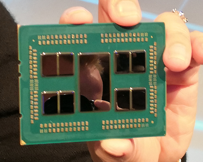
Nine crystals. Nine, damn it! The reasons for this decision are clear to me, and they are very simple: for the sake of increasing the yield of whole chips, lowering the total cost of the processor and speeding up development. 7 nm is still a raw process. Intel, with its 10 nm (+ - equal to 7 nm process TSMC) already from this ogrebla. So much so that we still saw 10 nm processors only as a single model of i3 stub notebook.
The central crystal is made on a proven 14 nm process and operates as a memory controller and all I / O except for PCIe 4.0, 16 lines of which are provided by each of the satellite crystals with eight cores on each.
One common memory controller provides the main thing - uniform memory access (UMA). And he will never be over.
Time speculation
The central crystal is connected to the satellites with the help of Infinity Fabric, which in turn gives a huge number of possibilities to use the components both together and separately. Need a desktop processor with 16 cores? We saw the crystal with a dual-channel memory controller and connect it with two nuclear complexes under one lid. Need a processor with integrated graphics? We throw out one nuclear complex, put the GPU chip instead. The cost of expanding the nomenclature of processors will decrease by an order of magnitude. A reduction in the size of individual crystals reduces the percentage of marriage, which in turn has a positive effect on the cost.
MOAR geek porn
What I have not written, but it is worth mentioning: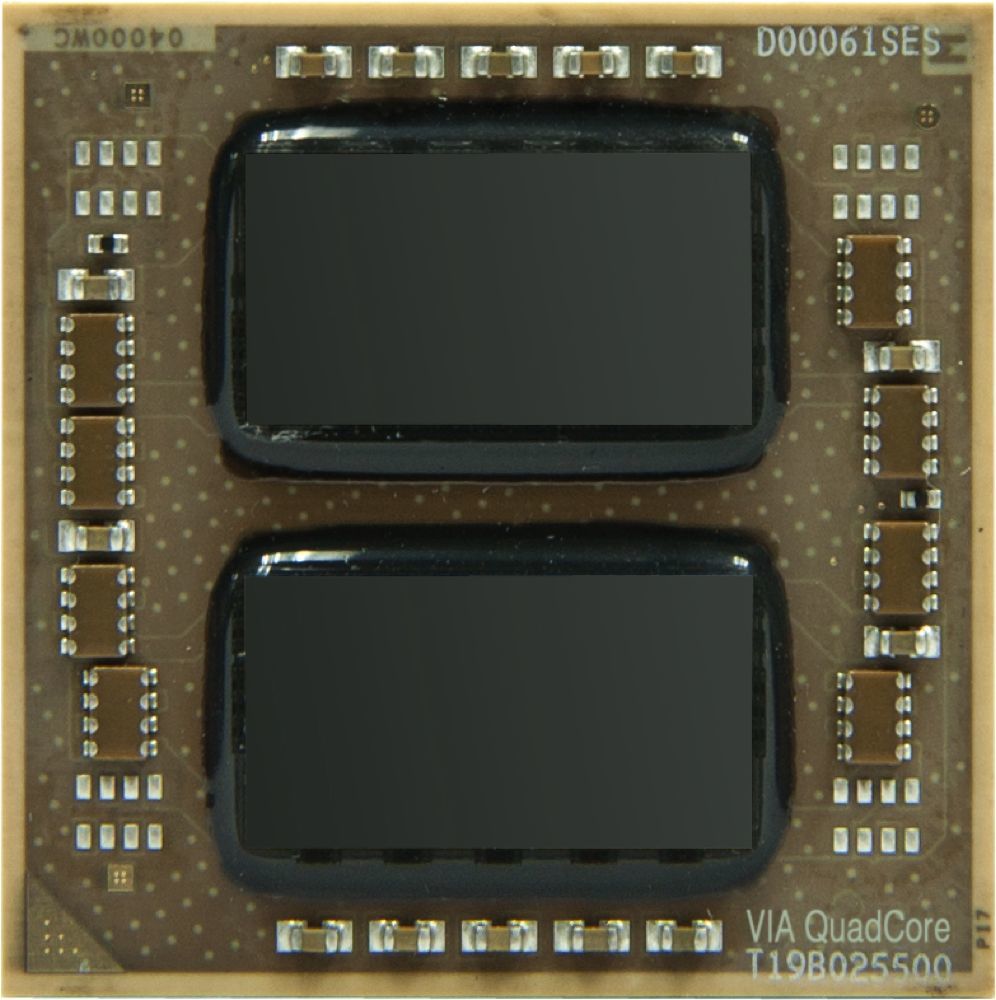
Via Nano QuadCore, completely forgot about it. He had nothing to do with her, there was nothing to tell.
IBM CPU 9121/311

IBM Power 5
And more than the new Power 7
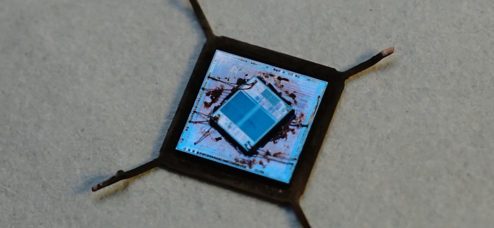
GD32 Microcontroller, on top of the flash memory chip. Photo from friend BarsMonster
Via Nano QuadCore, completely forgot about it. He had nothing to do with her, there was nothing to tell.
IBM CPU 9121/311
IBM Power 5
And more than the new Power 7
GD32 Microcontroller, on top of the flash memory chip. Photo from friend BarsMonster