Outputting images from the OV7670 camera to a VGA monitor using FPGA
Foreword
After reading many fascinating articles about interesting FPGA developments, such as Tetris , a radio transmitter and others , I also got the idea to do something for the soul. For this purpose, I purchased an OV7670 camera and a Terasic DE-1 debug board with an Altera Cyclone II chip. The task was as follows: display the image from the camera on a VGA monitor. In order to justify the use of FPGA, I am going to do it at the maximum speed for the camera. I must say that knowledge in the field of electronics will help to understand this work easier: knowledge of VGA and I2C interfaces, understanding of SDRAM memory, etc.
Introduction
This article is not a study, but rather a progress report in which I tried to show the main idea and the most interesting and complex places in my opinion. In terms of complexity, this project follows the “blink LED”, but has huge potential for expansion. The project intentionally does not use ready-made IP kernels and standard interfaces, since the project was originally planned as a handwritten one. Also, it will help to win a little in terms of resources and speed. I hope this article will be interesting to readers, and the desire to see themselves on the screen through a "home-made camera" will encourage the study of FPGA.
Disclamer
In some places in the project, the architecture and syntax of the code may not be optimal. This is due to the fact that I was engaged in the implementation of the project in my free time, and sometimes there were breaks between the approaches for several months: old thoughts were forgotten, but new ones appeared. So, for example, the central automaton was greatly simplified: only the name “global” remained from the original monster. Before publishing, I refactored the code, but if any flaws are found, please indicate them in the comments.
Problems and solutions
In order to understand what awaits us, take a look at the hardware and evaluate what problems we face. Camera OV7670. The camera is capable of producing an image with a resolution of 640x480 pixels with a frequency of 30 frames per second in RGB565 format. For the camera to work, it is necessary to apply a 24 MHz clock to it. The camera transmits data to the user via an 8-bit bus, as well as synchronization gates VSYNC and HSYNC. Timing diagrams of the camera are shown in Figure 1.

Fig . 1
Color information is transmitted over 2 cycles byte-by-bit. Packing data into bytes is shown in Figure 2.
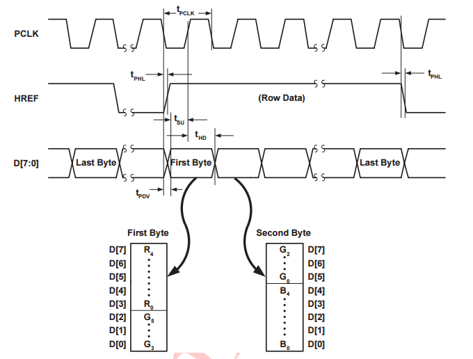
Figure 2
VGA monitor. VGA is an analog signal, therefore, it will not work to supply digital data to its input. But on board the DE-1 there are 4-bit DACs, we use them to convert a digital signal to an analog one. VGA with a resolution of 640x480 has a refresh rate of 60 frames per second. It is necessary to set data on the DAC with a frequency of 25.175 MHz, as well as to form synchronization gates VSYNC and HSYNC. The timings for VGA can be seen here .
It becomes clear that the frequency of data received from the camera and the frequency of data output to the monitor are different, which eliminates the possibility of direct connection. The way out of this situation is to use a frame buffer.. We select two equal areas in the memory: the current frame from the camera will be recorded in one, and the previous one will be extracted from the second, after the end of the recorded frame, the buffers will be swapped. To store one frame, 640 * 480 * 16 = 4.915 * 10 ^ 6 bits are required, which is much more than the on-chip memory available on board the Cyclone II. Therefore, we will use SDRAM , located by a separate chip on the DE-1 board , to store frames . This will allow us to organize a frame buffer for solving a technical problem and give us the opportunity to practice writing an SDRAM controller.
The next problem arises from the solution to the previous one. When using SDRAM in our project, two important points must be taken into account: firstly, the memory operates at a high frequency of 120 MHz for our design and we are faced with a new problem - transferring data from the camera’s domain to the SDRAM domain; secondly, to achieve maximum performance, writing in SDRAM should be with whole transactions, which are called burst. To solve these problems, FIFO, organized in an on-chip FPGA memory, is best suited. The basic idea is this: the camera at low frequency fills FIFO, after which the SDRAM controller reads the data at high frequency and immediately writes it to memory in one transaction.
Data output to the monitor is organized by the same principle. Data from the SDRAM is written to the FIFO, and then extracted at a frequency of 25 MHz for feeding to the DAC. After emptying the FIFO, the operation is repeated.
The smallest problem is that the camera settings “out of the box” do not suit us, and we need to change them. The most important point, the camera outputs data in the YUV422 format, and you need to change it to RGB444. To access the OV7670 internal registers, you will need to describe the I2C transmitter module.
Now we can say which modules we will have to implement, and what tasks they will solve.
- cam_wrp - the module receives data from the camera and writes it to the input FIFO;
- hvsync - the module generates strobes for VGA, receives data from SDRAM, writes it to the input FIFO and feeds it to the DAC along the strobe;
- sdram_cntr - SDRAM controller;
- FSM_global - automatic control;
- camera_configure - module for configuration and camera control.
Figure 3 shows the functional diagram of the design.
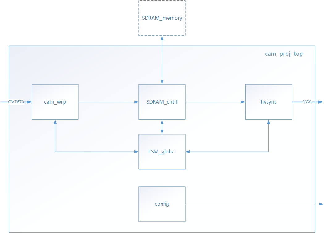
Fig. 3
Let us consider in more detail each of the modules.
Cam_wrp module
One of the easiest modules. Its task at the moment of operation of the hsync strobe of the camera is to take two bytes in succession, form one double-byte word from them and write it in FIFO. By the signal from the controller's SDRAM, transfer all the contents of the FIFO to it.
To “pack” 2 consecutive bytes in one word, we use the wr_fifo signal, which we invert by clock (divide the frequency by 2). When this signal is in logical 1, we write data in the low byte, when in the logical 0 it is written in the high byte. We also use wr_fifo as a write signal in FIFO. In addition to the data bus, a bus is displayed from the FIFO, on which the number of data written to it is set. This bus is connected to the control unit. Figure 4 shows the timing diagram of “packing” bytes into double-byte words.

Fig. 4
FSM_global module
The module has a very pathos name, in fact it is a simple automaton with only 4 states, but it performs a very important function. Tracking the readiness signal sd_ready SDRAM of the controller, the fullness of the input and output FIFO, the machine issues the SDRAM commands to the controller to collect data from the input or write to the output FIFO. Reading and writing occurs somewhat earlier than the FIFO is completely full or empty. It is necessary to choose the correct FIFO fill level so that operations with FIFOs at a high frequency do not end earlier than at a low frequency - this is guaranteed to lead to errors. In the part on the SDRAM controller, I will give a picture illustrating this feature.
SDRAM_contr module
A lot of SDRAM controllers have already been written, I did not want to reinvent the wheel again, so I decided to invent a caterpillar bike. Namely, the SDRAM controller, sharpened for this specific project. This will simplify management and speed things up a bit. The transition graph of the automaton for a full-fledged SDRAM controller is shown in Figure 5.

Fig.5.
We think that we can exclude from it.
First, we will not refresh the data. This assumption is absolutely not suitable for a general-purpose controller, but in our case we use the same memory area, constantly referring to it. Data will not have time to degrade.
Secondly, since we will always write and read data with a vector of length 640, we can refuse the possibility of working with individual numbers, we will write only burst.
Thirdly, we don’t have to think about the address, we will just increment it after each burst and zero at the end of each frame. The resulting transition graph shown in Figure 6.
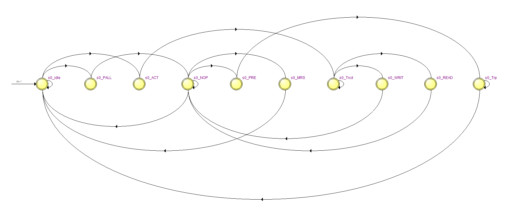
Figure 6
The controller starts in idle state. Before starting normal operation, it is necessary to initialize the memory chip (state of the machine s0_MRS), after which the mode_flag flag is set, the controller enters the standby state, and we can write and read data. To do this, the fsm_global module receives a command to start reading or writing, open the necessary column in the selected bank (state s0_ACT), and then read or write (state s0_WRIT, s0_READ). Unfortunately, one burst will not work, the column depth in our memory chip is only 256 16-bit words, and we need to write a vector with a length of 640. We have to write for 3 burst, two of 256 and one of 128. It can be seen that half of the third the line remains empty, that is, we are irrationally using resources, but since we have no shortage of them,
As for the addresses, different registers for reading and writing are allocated for them, which are incremented before each bust. Thus, to write a vector with a length of 640, we go through 640 * 4 = 1440 addresses. The vertical sync gate of the camera or VGA addresses are reset to write and read, respectively.
We use double buffering: we write to one buffer and read from another. To simplify, I placed one buffer in bank 0, and the second in bank 1 of the SDRAM chip. Banks for reading and writing change places after the end of the frame from the camera. Figure 7 shows the timing diagrams of recording a single vector. It can be seen that the record is divided into 3 parts: after each address is incremented, the entire transfer occurs under the strobe cur_wr. For reading, the diagram is similar.

Fig. 7
Figure 8 shows how the data from the camera is recorded in SDRAM in comparison with the FIFO filling time. Please note that we start writing in SDRAM without waiting for the final FIFO to be filled.

Fig. 8
Hvsync module
This is one of two modules in this project, not written by me. Once I already implemented a similar module, I was not interested in repeating, so I used an excellent module written by the authors of the site marsohod.org . There is nothing superfluous in this module, it is parameterized and can easily be configured for any screen resolution. I practically did not change it, I added only FIFO, connected to the SDRAM controller, and binding signals for it. A bus is displayed with FIFO, on which the amount of data recorded in it is set, this bus is connected to the control unit by analogy with the input FIFO. The FIFO output is connected to the wire that goes to the DAC.
Camera_configure module
Initially, taking the liberty of a home project and inattentively reading the documentation, I wanted to start the camera with the “default” settings, but it turned out that without the OV7670, it sends information in the format not RGB565, but to YUV422. I didn’t want to rewrite anything, and I decided that I should do everything wisely and properly initialize the camera. Since the camera is controlled by I2C, the idea came up with using NIOS. I couldn’t get NIOS with I2C peel with opencore from half a kick, but I accidentally stumbled upon Verilog's initialization moduleand it is for the OV7670. It was so easily integrated into the code that it did not have to change anything, changed only one line: instead of RGB565, it activated the RGB444 mode, since the board has exactly 4 bit DACs. Figure 9 shows the time diagram of the software reset of the camera by writing the number 0x80 to the address 0x12.

Fig. 9
Demonstration of the result
After all the modules are written, connect them together in the top module, assemble them in Quartus, and you can test. The video shows the result.
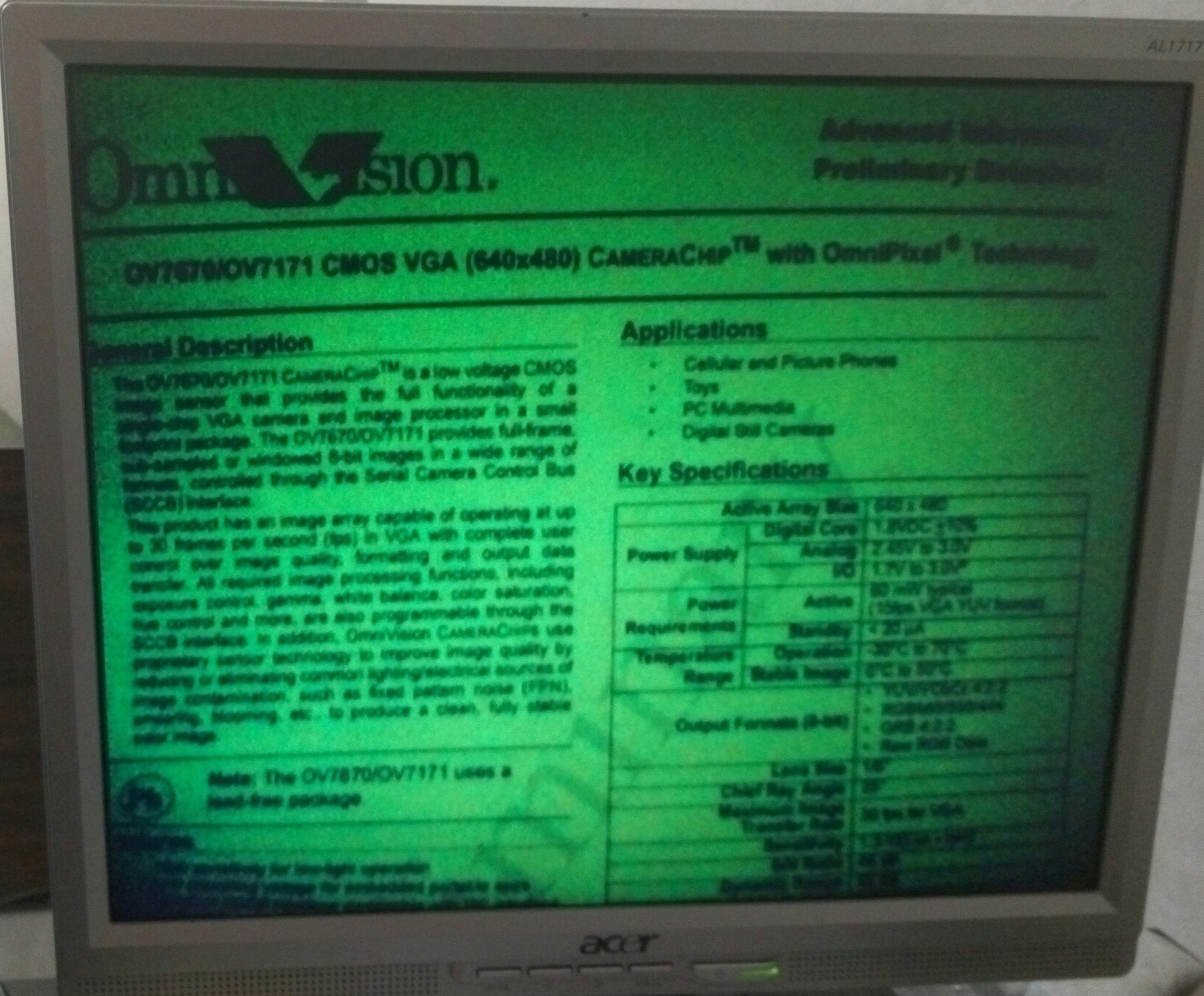
I chose a not very good time for shooting - sunset and very bright sun - the camera inadequately responds to too bright sun glare. It is seen that moving objects are displayed correctly, there are no twitches or loops. This is exactly what I achieved using FPGA, which allows me to process all 30 (and the camera’s capabilities more) fps with little blood. If we talk about the clarity of the image, I can say that the text from the A4 sheet is read without difficulties, unfortunately, the photos from the monitor are worse than in reality. Figure 10 shows a fragment of sheet A4 with documentation for the camera.
 "
" There are some flaws in the videos and photos presented: the first with sharpness and the second with color.
I connect the problem with sharpness in the video with imperfectly set focus. The focus is mechanically adjusted on the camera by screwing or unscrewing the lens located on the thread. The thread is plastic and has a fairly large backlash, even from a little shaking, the sharpness can deteriorate.
The problem with the excessive green and yellow of the white sheet, it seems to me, is connected with the problem with the white balance: the shooting was carried out in a room with lighting far from natural. Also, the camera settings can affect the color situation. I practically did not experiment take it off, used it as a magic number.
Conclusion
The task - the output of the image from the OV7670 camera to the VGA monitor in real time - has been solved. If we compare the result obtained in this project with the result obtained by other developers using microcontrollers or Arduino, we see that they are inferior in the speed of displaying moving objects. For the complexity of this project does not exceed similar ones made using a microcontroller. A person with an initial knowledge of FPGA design can implement it in a few days. The project has great potential for expansion, it is possible to filter the resulting image, object recognition and more. The design on the Cyclone II chip takes the following resources: LE - 745 (4%), memory bits - 32768 (14%), PLL - 1 (25%), Embedded Multiplier - 0 (0%), - thus
Afterword
What's next? In the future, I plan to expand the project by adding real-time image processing using matrix filters .
I express gratitude to ishevchuk for advice on the content and design of the article and to my girlfriend for spelling.
Bad duplicates
When you first turn on the screen, mysterious patterns appeared. I thought for a long time what it could be. As a result, it turned out that the focus was not set in the camera. After I twisted the lens on the lens, everything fell into place.
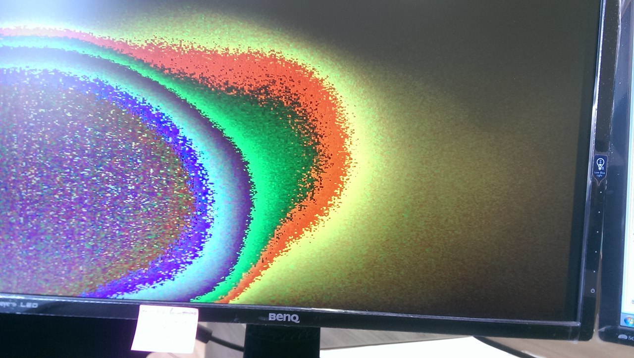 "alt =" image "/>
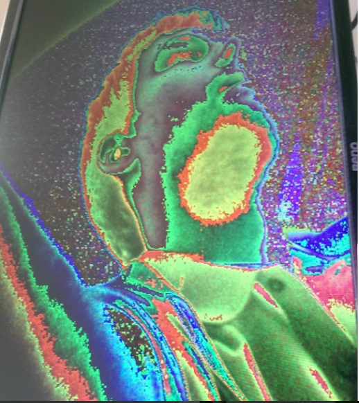
The second time it was turned on, the camera was improperly initialized, which led to an unexpected selfie.
 "
"
"alt =" image "/> The second time it was turned on, the camera was improperly initialized, which led to an unexpected selfie.
"You can download the archive with the sources here (Ya.Disk) .