August 12, 2015 at 00:16
CPLD retrocomputing. Part 1 - Student Board
Retrocomputing is different. Someone collects kilograms of ancient processors, someone restores the Soviet EU computers, someone still accelerates Celeron in liquid nitrogen, and we will enjoy the 1997 Altera University Programm Board UP1 board with the ancient CPLD MAX7128S and even blink the LED (and Not only).
Altera MAX (Multiple Array matriX) without numbers is a series of ancient CPLDs from Altera. This series was started back in 1993 (more than 20 years ago!) And is no longer being produced; it has been completely replaced by the MAX II, MAX V and even MAX 10 series. At the same time, the MAX7000 was first released, then the “big” ones MAX9000, then the “sophisticated” MAX5000 and the “cheap-low voltage” MAX3000. Then they added different letters S, E, B for JTAG, low-power and low-voltage versions, etc., in general, see the documentation.
We will be interested in the version of MAX7000S , which is distinguished by the presence of a JTAG port, that is, it implements the possibility of "programming in the system" through the built-in IEEStd interface. 1149.1 Joint Test Action Group (JTAG).
By the way, the first MAX7000 (without S) were programmed with a special hardware programmer and are practically not suitable for DIY applications.
To promote its product, Altera chose a simple and error-free method: in 1997 they announced the Altera University Program and began to distribute the debugging fee among (American) universities cheaply. The board is called Altera UP1 (from the University Programm). A little later, the second revision was released - Altera UP2, on which the wiring was slightly changed and a more capacious FLEX chip was soldered (more about it below).
Link from WebArchive about this board. (It has already been deleted on the "parent" site.) I
must say that Altera’s idea was a success. Dozens of universities have done laboratory work on this board for the courses "High-Speed Development of Digital Electronics", etc. Googling on "Altera UP1" and "UP2" still gives a bunch of links, including even video courses.
One of the most complete resources: users.ece.gatech.edu/~hamblen/ALTERA/altera.htm
Another review: www.pyroelectro.com/tutorials/up2 The
popularity of the board in the early 2000s was so high that even several books came out , who mentioned this board (Google Altera UP1 book), and the book " Rapid Prototyping of Digital Systems " by James O. Hamblen and Michael D. Furman is entirely built around this board, and can be considered as an extension of the documentation. (Those who wish will find in two clicks). The book, by the way, has survived several reprints, but starting with Edition 3 (SOPC Edition), it is based around Terasic DEx boards, also loved by drawers, but which do not fall under the prefix retro
Finally, in the 2010s, the board was completely out of date, they began to be written off from universities and they began to appear on e-bay for ridiculous money, where, in fact, a couple of such boards were purchased. There is a fly in the ointment - alas, students (even American ones) are not accurate, so beaten I / O pins on such second-hand boards are not uncommon, and the CPLD recording resource is worn out. So the chip may be slightly burnt, it is better to replace it immediately, since it is in the PLCC84 socket.
Deep google gives a bunch of links to university resources from different countries, from Japan to Poland, which shows how much the board has spread. It is not known for certain whether the UP1 board was used so widely in Russia, but on the website of the St. Petersburg LIAP (forgive me the old name) was a manual in Russianwith a description of the board for some laboratory work. If anyone else used the board in other universities, let me know, interesting.
Now a few words about the board itself. In addition to the CPLD EPM7128S, the old FPGA FLEX 10K chip is also soldered to it, there is a DIP-8 panel for Configuration Memory, but for some reason the EPC1 chip is not included in the kit (maybe because it is disposable). The FLEX 10K chip is pretty decent even by modern standards, especially on the Altera UP2 board - EPF10K70. As usual, there is a power stabilizer, two pairs of 7-segment indicators, quartz at 25.175 MHz, buttons, switches and just LEDs (you can blink!). VGA and PS / 2 mouse sockets are soldered to FLEX, you can even make video games, but this is not about FLEX.
An old luxurious LPT-shined JTAG Altera ByteBlasterMV (MV from the word MultiVolt) is attached to the board. By the way, if you take on e-bay, require the presence of ByteBlaster. True, why is it in the age of USB and in the absence of LPT - it is not clear, but there must be a complete set.
Since the word "retrocomputing" was uttered, yes, I must admit that the attention to the MAX7000S was caused precisely in the aspect of applying it to integrate into retro computers, for example, to attach something to the BK-0010 or Mikroshi. And the reason for the interest here is very simple: 5 volts TTL. It is clear that the era has changed and low-voltage progress cannot be stopped, but retro- and progress things, mmmm ... are incompatible ...
One way or another, at present, 5-volt CPLDs and FPGAs have practically disappeared. The MAX7000S family is no longer recommended for use and is no longer available, as well as the competing Xilinx XC9500 series (without XL). Newer CPLDs are already “5-volt tolerant”, that is, at best, they do not burn at the input of 5 volts, but the output is still 3.3 volts, and on site 6502.org there was information that some older processors did not work with 3.3 volt pins.
MAX7000S can still be bought on e-bay / aliexpress not expensively, but these are stock leftovers or frankly used chips. Once I received a pretty scratched case PLCC84, but 6 pieces, although it was ordered 5. The Chinese also perfectly understand what they are selling.
Altera UP1 courses recommend that you program it using the ancient MAX + PLUS II program, brutally draw circuits from 2I-NOT and D-flip-flops, and flash Altera ByteBlaster programmer on the LPT port. This, of course, is all great, but do not confuse retro computing and masochism. Each duct is deployed with Quartus II and has a USB Blaster. If not, then its prices have fallen so much that a USB-Blaster clone on aliexpress costs less than $ 5 and is undoubtedly recommended for purchase. Again, useful for DE2, etc. (Blasters will be discussed a bit later).
As for Quartus II, the latest version is 13.0 to support the MAX7000S and Web Edition is quite suitable. There is a little cutback in functionality, for example, the compiler does not support multicore, etc., but this is not critical for us. The author generally deployed Quartus II 11.0 SP1 and everything works.
So, we will program on the modern VHDL, in the (almost) modern Quartus II and flash through the (almost) modern USB-Blaster. And all this on the retro MAX7000S. As they say, hardware is retro, and software is with amenities.
There are plenty of articles on CPLD / FPGA programming on the network, for example on we.easyelectronics.ru in the FPGA hub , and there were almost a dozen of them on the dying Habr. Ideologically close, for example, the board of the Mars rover projectThere is only CPLD newer. So the tutorials of the Mars rover are quite useful to us.
The project is nothing special: we will make a hexadecimal timer with a 7-LED display, since it is already soldered on the board. In addition, we will flash a decimal point. Resources at CPLD are very limited, there are only 128 macro-cells in the MAX7128S, so we will constantly check ourselves, looking at the resulting RTL and paying attention to the amount of resources used up.
First, you need to get a meander with a period of about a second, not necessarily for sure, it's a demo. We need a counter with a rather large conversion factor to divide 25.175MHz from quartz. You can divide, for example, by 2 ^ 24 = 16777216 and get a frequency of about 1.5 hertz. The classic synchronous counter +1 is not suitable here, because Quartus generates a giant 24-bit adder, the constant “1” is applied to one input. Tin. We make an ordinary divider from the chain of D-triggers, spending 24 cells, the so-called ripple-counter. Grammar-design-nazi will say this is a bad style, clock pulses must go through global blocks, the counter must be synchronous, etc. To which we will answer simply - give us a PLL or not to put such a high-frequency quartz.
To generate a long chain of triggers, use the VHDL GENERATE construct. This is such a disguised macro operator of the VHDL language and you can do funny things with it, but everything is simple with us.
Top-level design is extremely primitive. Here we will make a classic 8-bit counter, purelyneighing to be horrified by the received RTL implementation with an adder. But in real life, everything is not so bad, the counter eats exactly 8 macrocells, but the adder is impressive, although it fits into the standard logical part of the macrocells within the logical block. Compiler offset.
The 7-segment decoder does not cause problems and is synthesized into ordinary logic circuits with honest warm 5-volt pins for LEDs, although it eats a macro cell for each pin.
Result:
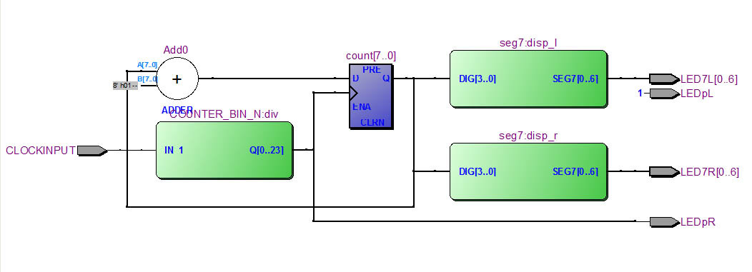
Do not forget to bind the output pins. For assignment, you can use the Pin Planner editor, but you can hardcore edit the text .QSF file. There is only one, perhaps, subtlety - the order of bits in the array, depending on the declaration of its TO or DOWNTO. Here you can see that the input goes to the DOWNTO side for compatibility with counter bits (DOWNTO has the lowest bit on the right) and the output to the 7-segment indicator is TO for compatibility with documentation. You can also make it DOWNTO, but then you have to redefine the pin numbers.
Result: Logic cells; 47/128 (37%)
The CPLD MAX7128S firmware does not cause any problems; replacing the standard Altera ByteBlasterMV with the Altera USB Blaster runs smoothly, both from the point of view of Quartus II and from the point of view of the Altera UP1 board. The JTAG connector has exactly the same pinout, and the VCC pin indicates the voltage of the JTAG port. Actually, that's why ByteBlasterMV wore the prefix Multi Volt. The ability to work with different voltages USB Blaster inherited from ByteBlasterMV.
Altera Byte Blaster programmers and their clones have been written a lot and in detail.
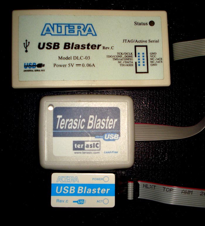
The first two are almost standard Altera USB Blaster, and Terasic (or its clone, who will understand) generally seems to be licensed. As you know, the "classic" USB Blaster is assembled according to the scheme "FT245BM + CPLD + buffer" as described in the manual.
The latter is a real Chinese miracle (more precisely, Japanese-Chinese). This is the FT245BM + CPLD emulator on the cheap PIC18F14K50. Nevertheless, Quartus II recognizes this “fake” as a native USB Blaster and the firmware function via JTAG works. It is surprising that even the proprietary FTDI FT Prog finds the FT245BM chip and reads something from it.
Here is a description of the insides of this Chinese clone emulator.
So, we were in the shoes of a student ~ 2007, while using the VHDL and USB Blaster for CPLD firmware. The board is quite useful for joining the CPLD course, it competes with the LC Tech CPLD and FPGA boards , which are clogged with aliexpress and it is quite worth buying if you see it is not expensive. Literature and courses on it a huge amount. The board works with the standard TTL 5 volts and mates well with older devices. Do not forget to buy a stock of MAX7128S - the resource is not eternal.
In the next part, we will try to replace the MAX7128S with an Atmel ATF1508AS which is supposedly compatible and see what happens.
Max, what is it?
Altera MAX (Multiple Array matriX) without numbers is a series of ancient CPLDs from Altera. This series was started back in 1993 (more than 20 years ago!) And is no longer being produced; it has been completely replaced by the MAX II, MAX V and even MAX 10 series. At the same time, the MAX7000 was first released, then the “big” ones MAX9000, then the “sophisticated” MAX5000 and the “cheap-low voltage” MAX3000. Then they added different letters S, E, B for JTAG, low-power and low-voltage versions, etc., in general, see the documentation.
We will be interested in the version of MAX7000S , which is distinguished by the presence of a JTAG port, that is, it implements the possibility of "programming in the system" through the built-in IEEStd interface. 1149.1 Joint Test Action Group (JTAG).
By the way, the first MAX7000 (without S) were programmed with a special hardware programmer and are practically not suitable for DIY applications.
Altera UP1
To promote its product, Altera chose a simple and error-free method: in 1997 they announced the Altera University Program and began to distribute the debugging fee among (American) universities cheaply. The board is called Altera UP1 (from the University Programm). A little later, the second revision was released - Altera UP2, on which the wiring was slightly changed and a more capacious FLEX chip was soldered (more about it below).
Link from WebArchive about this board. (It has already been deleted on the "parent" site.) I
must say that Altera’s idea was a success. Dozens of universities have done laboratory work on this board for the courses "High-Speed Development of Digital Electronics", etc. Googling on "Altera UP1" and "UP2" still gives a bunch of links, including even video courses.
One of the most complete resources: users.ece.gatech.edu/~hamblen/ALTERA/altera.htm
Another review: www.pyroelectro.com/tutorials/up2 The
popularity of the board in the early 2000s was so high that even several books came out , who mentioned this board (Google Altera UP1 book), and the book " Rapid Prototyping of Digital Systems " by James O. Hamblen and Michael D. Furman is entirely built around this board, and can be considered as an extension of the documentation. (Those who wish will find in two clicks). The book, by the way, has survived several reprints, but starting with Edition 3 (SOPC Edition), it is based around Terasic DEx boards, also loved by drawers, but which do not fall under the prefix retro
Finally, in the 2010s, the board was completely out of date, they began to be written off from universities and they began to appear on e-bay for ridiculous money, where, in fact, a couple of such boards were purchased. There is a fly in the ointment - alas, students (even American ones) are not accurate, so beaten I / O pins on such second-hand boards are not uncommon, and the CPLD recording resource is worn out. So the chip may be slightly burnt, it is better to replace it immediately, since it is in the PLCC84 socket.
Deep google gives a bunch of links to university resources from different countries, from Japan to Poland, which shows how much the board has spread. It is not known for certain whether the UP1 board was used so widely in Russia, but on the website of the St. Petersburg LIAP (forgive me the old name) was a manual in Russianwith a description of the board for some laboratory work. If anyone else used the board in other universities, let me know, interesting.
Now a few words about the board itself. In addition to the CPLD EPM7128S, the old FPGA FLEX 10K chip is also soldered to it, there is a DIP-8 panel for Configuration Memory, but for some reason the EPC1 chip is not included in the kit (maybe because it is disposable). The FLEX 10K chip is pretty decent even by modern standards, especially on the Altera UP2 board - EPF10K70. As usual, there is a power stabilizer, two pairs of 7-segment indicators, quartz at 25.175 MHz, buttons, switches and just LEDs (you can blink!). VGA and PS / 2 mouse sockets are soldered to FLEX, you can even make video games, but this is not about FLEX.
An old luxurious LPT-shined JTAG Altera ByteBlasterMV (MV from the word MultiVolt) is attached to the board. By the way, if you take on e-bay, require the presence of ByteBlaster. True, why is it in the age of USB and in the absence of LPT - it is not clear, but there must be a complete set.
Warm 5 volt
Since the word "retrocomputing" was uttered, yes, I must admit that the attention to the MAX7000S was caused precisely in the aspect of applying it to integrate into retro computers, for example, to attach something to the BK-0010 or Mikroshi. And the reason for the interest here is very simple: 5 volts TTL. It is clear that the era has changed and low-voltage progress cannot be stopped, but retro- and progress things, mmmm ... are incompatible ...
One way or another, at present, 5-volt CPLDs and FPGAs have practically disappeared. The MAX7000S family is no longer recommended for use and is no longer available, as well as the competing Xilinx XC9500 series (without XL). Newer CPLDs are already “5-volt tolerant”, that is, at best, they do not burn at the input of 5 volts, but the output is still 3.3 volts, and on site 6502.org there was information that some older processors did not work with 3.3 volt pins.
MAX7000S can still be bought on e-bay / aliexpress not expensively, but these are stock leftovers or frankly used chips. Once I received a pretty scratched case PLCC84, but 6 pieces, although it was ordered 5. The Chinese also perfectly understand what they are selling.
Programming with all the amenities
Altera UP1 courses recommend that you program it using the ancient MAX + PLUS II program, brutally draw circuits from 2I-NOT and D-flip-flops, and flash Altera ByteBlaster programmer on the LPT port. This, of course, is all great, but do not confuse retro computing and masochism. Each duct is deployed with Quartus II and has a USB Blaster. If not, then its prices have fallen so much that a USB-Blaster clone on aliexpress costs less than $ 5 and is undoubtedly recommended for purchase. Again, useful for DE2, etc. (Blasters will be discussed a bit later).
As for Quartus II, the latest version is 13.0 to support the MAX7000S and Web Edition is quite suitable. There is a little cutback in functionality, for example, the compiler does not support multicore, etc., but this is not critical for us. The author generally deployed Quartus II 11.0 SP1 and everything works.
So, we will program on the modern VHDL, in the (almost) modern Quartus II and flash through the (almost) modern USB-Blaster. And all this on the retro MAX7000S. As they say, hardware is retro, and software is with amenities.
There are plenty of articles on CPLD / FPGA programming on the network, for example on we.easyelectronics.ru in the FPGA hub , and there were almost a dozen of them on the dying Habr. Ideologically close, for example, the board of the Mars rover projectThere is only CPLD newer. So the tutorials of the Mars rover are quite useful to us.
The project is nothing special: we will make a hexadecimal timer with a 7-LED display, since it is already soldered on the board. In addition, we will flash a decimal point. Resources at CPLD are very limited, there are only 128 macro-cells in the MAX7128S, so we will constantly check ourselves, looking at the resulting RTL and paying attention to the amount of resources used up.
First, you need to get a meander with a period of about a second, not necessarily for sure, it's a demo. We need a counter with a rather large conversion factor to divide 25.175MHz from quartz. You can divide, for example, by 2 ^ 24 = 16777216 and get a frequency of about 1.5 hertz. The classic synchronous counter +1 is not suitable here, because Quartus generates a giant 24-bit adder, the constant “1” is applied to one input. Tin. We make an ordinary divider from the chain of D-triggers, spending 24 cells, the so-called ripple-counter. Grammar-design-nazi will say this is a bad style, clock pulses must go through global blocks, the counter must be synchronous, etc. To which we will answer simply - give us a PLL or not to put such a high-frequency quartz.
To generate a long chain of triggers, use the VHDL GENERATE construct. This is such a disguised macro operator of the VHDL language and you can do funny things with it, but everything is simple with us.
Counter
library ieee;
use ieee.std_logic_1164.all;
use ieee.std_logic_unsigned.all;
entity D_FF is
-- Flipflop
port (D,CLK_S	: in std_logic;
		Q			: buffer std_logic := '0';
		NQ			: out std_logic := '1' );
end entity D_FF;
architecture A_RS_FF of D_FF is
begin
BIN_P_RS_FF:
	process(CLK_S) begin
		if CLK_S = '1' and CLK_S'Event
			then	Q  <= D;
		end if;
	end process;
NQ <= not Q;
end architecture A_RS_FF;
library ieee;
use ieee.std_logic_1164.all;
use ieee.std_logic_unsigned.all;
-- Couner
entity COUNTER_BIN_N is generic (N : integer := 24);
port (Q		: out std_logic_vector(0 to N-1);
		IN_1	: in std_logic );
end entity COUNTER_BIN_N;
architecture BEH of COUNTER_BIN_N is
component D_FF
	port(D, CLK_S : in std_logic; Q, NQ : out std_logic);
end component D_FF;
signal S : std_logic_vector(0 to N);
begin
	S(0) <= IN_1;
	G_1 : for I in 0 to N-1 generate
		D_Flip_Flop : D_FF port map
						(D => S(I+1), CLK_S => S(I), Q => Q(I), NQ => S(I+1));
	end generate;
end architecture BEH;
Top-level design is extremely primitive. Here we will make a classic 8-bit counter, purely
Top level
library ieee;
use ieee.std_logic_1164.all;
use ieee.std_logic_unsigned.all;
use ieee.std_logic_arith.all;
entity UP1TEST is
	port (
		CLOCKINPUT		: in std_logic;
		LEDpL				: out	std_logic;
		LEDpR				: out std_logic;
		LED7L				: out	std_logic_vector(0 to 6);
		LED7R				: out std_logic_vector(0 to 6)
		);
end entity UP1TEST;
architecture rtl of UP1TEST is
	signal COUNTER		: std_logic_vector(7 downto 0);
	signal SLOWCLOCK	: std_logic;
	signal divider			: std_logic_vector(0 to 23);
begin
-- 27.175MHz ~~ 2^24
div:
	work.COUNTER_BIN_N port map (Q => divider, IN_1 => CLOCKINPUT);
SLOWCLOCK <= divider(23);
LEDpL <= '1';
LEDpR <= SLOWCLOCK;
process (SLOWCLOCK)
	variable count : natural range 0 to 255 := 0;
begin
	if rising_edge(SLOWCLOCK) then
			count := count + 1;
	end if;
	COUNTER <= conv_std_logic_vector(count,8);
end process;
disp_r:
	work.seg7 PORT MAP (DIG => COUNTER(3 downto 0), SEG7 => LED7R);
disp_l:
	work.seg7 PORT MAP (DIG => COUNTER(7 downto 4), SEG7 => LED7L);
end rtl;
The 7-segment decoder does not cause problems and is synthesized into ordinary logic circuits with honest warm 5-volt pins for LEDs, although it eats a macro cell for each pin.
7-LED decoder
library ieee;
use ieee.std_logic_1164.all;
use ieee.std_logic_unsigned.all;
entity seg7 is
	port (
		DIG	: in	std_logic_vector(3 downto 0);
		SEG7	: out	std_logic_vector(6 downto 0));
end entity seg7;
architecture rtl of seg7 is
begin
with DIG select
SEG7 <=	"1001111" WHEN "0001", -- 1 +--A--+
		"0010010" WHEN "0010", -- 2 |     |
		"0000110" WHEN "0011", -- 3 F     B
		"1001100" WHEN "0100", -- 4 |     |
		"0100100" WHEN "0101", -- 5 +--G--+
		"0100000" WHEN "0110", -- 6 |     |
		"0001111" WHEN "0111", -- 7 E     C
		"0000000" WHEN "1000", -- 8 |     |
		"0000100" WHEN "1001", -- 9 +--D--+
		"0001000" WHEN "1010", -- A
		"1100000" WHEN "1011", -- B
		"0110001" WHEN "1100", -- C
		"1000010" WHEN "1101", -- D
		"0110000" WHEN "1110", -- E
		"0111000" WHEN "1111", -- F
		"0000001" WHEN others; -- 0
end rtl;
Result:
Do not forget to bind the output pins. For assignment, you can use the Pin Planner editor, but you can hardcore edit the text .QSF file. There is only one, perhaps, subtlety - the order of bits in the array, depending on the declaration of its TO or DOWNTO. Here you can see that the input goes to the DOWNTO side for compatibility with counter bits (DOWNTO has the lowest bit on the right) and the output to the 7-segment indicator is TO for compatibility with documentation. You can also make it DOWNTO, but then you have to redefine the pin numbers.
QSF
# ------------------------------------------------- ------------------------- # # # Quartus II # Version 11.0 Build 208 03/03/2011 Service Pack 1 SJ Web Edition # Date created = 23:59:49 July 10, 2015 # # ------------------------------------------------- ------------------------- # # # Notes: # # 1) The default values for assignments are stored in the file: # UP1-TEST_assignment_defaults.qdf # If this file doesn't exist, see file: # assignment_defaults.qdf # # 2) Altera recommends that you do not modify this file. This # file is updated automatically by the Quartus II software # and any changes you make may be lost or overwritten. # # ------------------------------------------------- ------------------------- # set_global_assignment -name FAMILY MAX7000S set_global_assignment -name DEVICE "EPM7128SLC84-7" set_global_assignment -name TOP_LEVEL_ENTITY UP1TEST set_global_assignment -name ORIGINAL_QUARTUS_VERSION "11.0 SP1" set_global_assignment -name PROJECT_CREATION_TIME_DATE "23:59:49 JULY 10, 2015" set_global_assignment -name LAST_QUARTUS_VERSION "11.0 SP1" set_global_assignment -name ERROR_CHECK_FREQUENCY_DIVISOR "-1" set_global_assignment -name MAX7000_DEVICE_IO_STANDARD TTL set_global_assignment -name RESERVE_ALL_UNUSED_PINS_NO_OUTPUT_GND "AS INPUT TRI-STATED" set_global_assignment -name OPTIMIZE_HOLD_TIMING OFF set_global_assignment -name FITTER_EFFORT "STANDARD FIT" set_location_assignment PIN_83 -to CLOCKINPUT set_location_assignment PIN_58 -to LED7L [0] set_location_assignment PIN_60 -to LED7L [1] set_location_assignment PIN_61 -to LED7L [2] set_location_assignment PIN_63 -to LED7L [3] set_location_assignment PIN_64 -to LED7L [4] set_location_assignment PIN_65 -to LED7L [5] set_location_assignment PIN_67 -to LED7L [6] set_location_assignment PIN_68 -to LEDpL set_location_assignment PIN_69 -to LED7R [0] set_location_assignment PIN_70 -to LED7R [1] set_location_assignment PIN_73 -to LED7R [2] set_location_assignment PIN_74 -to LED7R [3] set_location_assignment PIN_76 -to LED7R [4] set_location_assignment PIN_75 -to LED7R [5] set_location_assignment PIN_77 -to LED7R [6] set_location_assignment PIN_79 -to LEDpR set_global_assignment -name VHDL_FILE counter.vhd set_global_assignment -name VHDL_FILE seg7.vhd set_global_assignment -name VHDL_FILE "UP1-TEST.vhd"
Result: Logic cells; 47/128 (37%)
Report on the disposal of ME
+ ------------------------------------------------- -------------------------------------------------- ------------------------ +
; Fitter Resource Utilization by Entity;
+ ---------------------------------- + ------------ + - ----- + -------------------------------------------- --------- + -------------- +
; Compilation Hierarchy Node; Macrocells Pins; Full Hierarchy Name; Library Name;
+ ---------------------------------- + ------------ + - ----- + -------------------------------------------- --------- + -------------- +
; | UP1TEST; 47; 21; | UP1TEST; work;
; | COUNTER_BIN_N: div | ; 24; 0; | UP1TEST | COUNTER_BIN_N: div; work;
; | D_FF: \ G_1: 0: D_Flip_Flop | ; 1 ; 0; | UP1TEST | COUNTER_BIN_N: div | D_FF: \ G_1: 0: D_Flip_Flop; work;
; | D_FF: \ G_1: 10: D_Flip_Flop | ; 1 ; 0; | UP1TEST | COUNTER_BIN_N: div | D_FF: \ G_1: 10: D_Flip_Flop; work;
; | D_FF: \ G_1: 11: D_Flip_Flop | ; 1 ; 0; | UP1TEST | COUNTER_BIN_N: div | D_FF: \ G_1: 11: D_Flip_Flop; work;
; | D_FF: \ G_1: 12: D_Flip_Flop | ; 1 ; 0; | UP1TEST | COUNTER_BIN_N: div | D_FF: \ G_1: 12: D_Flip_Flop; work;
; | D_FF: \ G_1: 13: D_Flip_Flop | ; 1 ; 0; | UP1TEST | COUNTER_BIN_N: div | D_FF: \ G_1: 13: D_Flip_Flop; work;
; | D_FF: \ G_1: 14: D_Flip_Flop | ; 1 ; 0; | UP1TEST | COUNTER_BIN_N: div | D_FF: \ G_1: 14: D_Flip_Flop; work;
; | D_FF: \ G_1: 15: D_Flip_Flop | ; 1 ; 0; | UP1TEST | COUNTER_BIN_N: div | D_FF: \ G_1: 15: D_Flip_Flop; work;
; | D_FF: \ G_1: 16: D_Flip_Flop | ; 1 ; 0; | UP1TEST | COUNTER_BIN_N: div | D_FF: \ G_1: 16: D_Flip_Flop; work;
; | D_FF: \ G_1: 17: D_Flip_Flop | ; 1 ; 0; | UP1TEST | COUNTER_BIN_N: div | D_FF: \ G_1: 17: D_Flip_Flop; work;
; | D_FF: \ G_1: 18: D_Flip_Flop | ; 1 ; 0; | UP1TEST | COUNTER_BIN_N: div | D_FF: \ G_1: 18: D_Flip_Flop; work;
; | D_FF: \ G_1: 19: D_Flip_Flop | ; 1 ; 0; | UP1TEST | COUNTER_BIN_N: div | D_FF: \ G_1: 19: D_Flip_Flop; work;
; | D_FF: \ G_1: 1: D_Flip_Flop | ; 1 ; 0; | UP1TEST | COUNTER_BIN_N: div | D_FF: \ G_1: 1: D_Flip_Flop; work;
; | D_FF: \ G_1: 20: D_Flip_Flop | ; 1 ; 0; | UP1TEST | COUNTER_BIN_N: div | D_FF: \ G_1: 20: D_Flip_Flop; work;
; | D_FF: \ G_1: 21: D_Flip_Flop | ; 1 ; 0; | UP1TEST | COUNTER_BIN_N: div | D_FF: \ G_1: 21: D_Flip_Flop; work;
; | D_FF: \ G_1: 22: D_Flip_Flop | ; 1 ; 0; | UP1TEST | COUNTER_BIN_N: div | D_FF: \ G_1: 22: D_Flip_Flop; work;
; | D_FF: \ G_1: 23: D_Flip_Flop | ; 1 ; 0; | UP1TEST | COUNTER_BIN_N: div | D_FF: \ G_1: 23: D_Flip_Flop; work;
; | D_FF: \ G_1: 2: D_Flip_Flop | ; 1 ; 0; | UP1TEST | COUNTER_BIN_N: div | D_FF: \ G_1: 2: D_Flip_Flop; work;
; | D_FF: \ G_1: 3: D_Flip_Flop | ; 1 ; 0; | UP1TEST | COUNTER_BIN_N: div | D_FF: \ G_1: 3: D_Flip_Flop; work;
; | D_FF: \ G_1: 4: D_Flip_Flop | ; 1 ; 0; | UP1TEST | COUNTER_BIN_N: div | D_FF: \ G_1: 4: D_Flip_Flop; work;
; | D_FF: \ G_1: 5: D_Flip_Flop | ; 1 ; 0; | UP1TEST | COUNTER_BIN_N: div | D_FF: \ G_1: 5: D_Flip_Flop; work;
; | D_FF: \ G_1: 6: D_Flip_Flop | ; 1 ; 0; | UP1TEST | COUNTER_BIN_N: div | D_FF: \ G_1: 6: D_Flip_Flop; work;
; | D_FF: \ G_1: 7: D_Flip_Flop | ; 1 ; 0; | UP1TEST | COUNTER_BIN_N: div | D_FF: \ G_1: 7: D_Flip_Flop; work;
; | D_FF: \ G_1: 8: D_Flip_Flop | ; 1 ; 0; | UP1TEST | COUNTER_BIN_N: div | D_FF: \ G_1: 8: D_Flip_Flop; work;
; | D_FF: \ G_1: 9: D_Flip_Flop | ; 1 ; 0; | UP1TEST | COUNTER_BIN_N: div | D_FF: \ G_1: 9: D_Flip_Flop; work;
; | lpm_counter: count_rtl_0 | ; 8 ; 0; | UP1TEST | lpm_counter: count_rtl_0; work;
; | seg7: disp_l | ; 7; 0; | UP1TEST | seg7: disp_l; work;
; | seg7: disp_r | ; 7; 0; | UP1TEST | seg7: disp_r; work;
+ ---------------------------------- + ------------ + - ----- + -------------------------------------------- --------- + -------------- +
Firmware
The CPLD MAX7128S firmware does not cause any problems; replacing the standard Altera ByteBlasterMV with the Altera USB Blaster runs smoothly, both from the point of view of Quartus II and from the point of view of the Altera UP1 board. The JTAG connector has exactly the same pinout, and the VCC pin indicates the voltage of the JTAG port. Actually, that's why ByteBlasterMV wore the prefix Multi Volt. The ability to work with different voltages USB Blaster inherited from ByteBlasterMV.
Altera Byte Blaster programmers and their clones have been written a lot and in detail.
The first two are almost standard Altera USB Blaster, and Terasic (or its clone, who will understand) generally seems to be licensed. As you know, the "classic" USB Blaster is assembled according to the scheme "FT245BM + CPLD + buffer" as described in the manual.
The latter is a real Chinese miracle (more precisely, Japanese-Chinese). This is the FT245BM + CPLD emulator on the cheap PIC18F14K50. Nevertheless, Quartus II recognizes this “fake” as a native USB Blaster and the firmware function via JTAG works. It is surprising that even the proprietary FTDI FT Prog finds the FT245BM chip and reads something from it.
Here is a description of the insides of this Chinese clone emulator.
Insides
Conclusion
So, we were in the shoes of a student ~ 2007, while using the VHDL and USB Blaster for CPLD firmware. The board is quite useful for joining the CPLD course, it competes with the LC Tech CPLD and FPGA boards , which are clogged with aliexpress and it is quite worth buying if you see it is not expensive. Literature and courses on it a huge amount. The board works with the standard TTL 5 volts and mates well with older devices. Do not forget to buy a stock of MAX7128S - the resource is not eternal.
In the next part, we will try to replace the MAX7128S with an Atmel ATF1508AS which is supposedly compatible and see what happens.