Measuring power consumption for digital ASIC chips (even before manufacturing)
- Tutorial
Recently on Habrahabr there were many articles devoted to development for FPGA / FPGA . This happened both with the direct participation of my colleagues and other users. It can be seen that such articles contribute to the popularization of this field of development and show that there is already substantial interest in the direction of hardware development in general (figuratively called "hardware").
In this article, I will enter the practically “untouched field” of development for ASIC and talk about one interesting aspect of creating digital parts ( IP-blocks ) in ASIC chips . This development area is even narrower than FPGA .
ASIC (application-specific integrated circuit) is an integrated circuit specialized to solve a specific problem.
My article illustrates the commonly used method of measuring power consumption for a single IP block inside a chip even before it can be measured in a manufactured chip. Such an assessment allows you at an early stage:
- Compare different versions of the digital data processing algorithm,
- choose the best option for implementation according to the criterion of consumption / digital loss,
- quite accurately estimate the power consumption in numbers when working in a chip released by a certain technology.
With this method, with some assumptions, one can quite accurately compare several implementations of the algorithm in HDL (digital circuit description language). In our case, it will be Verilog , which is the most popular development language for ASIC .
Two assumptions to speed up the process of comparing multiple implementations:
- I will not conduct a complete synthesis of the IP block to obtain the final layer-by-layer implementation (it includes all parasitic capacities that also affect consumption), but restrict myself to the so-called ideal wire-load model of the synthesized IP block . * A more accurate estimate in absolute numbers is obtained during synthesis in the extended topographical mode (with layered synthesis), but with a relative comparison this can be neglected.
- It will not be possible to evaluate and take into account the consumption of “shred tree” after wire-load synthesis. To evaluate it, you need to do a complete wiring in the crystal. In synchronous circuits, it can give a significant consumption in numbers relative to the consumption of the entire unit during operation. But when comparing different implementations of the block with approximately the same trigger area, we can consider the consumption of the “block tree” to be approximately the same.
What we need to measure consumption:
- Component Library (Standard Cell Library) for the target technology (130/90 / 65nm; provided by the manufacturer under the NDA )
- Program for synthesizing netlist from Verilog in the basis of the selected component library
- Consumption Estimation Program
- A program for simulating and logging the operating mode of our IP block (we want to get an accurate estimate of consumption in the operating mode, and not a statistical estimate of the consumption of the block)
In particular, I used Synopsys DC (Design Compiler) to synthesize and calculate consumption, and Modelsim to simulate work and log the number of signal switching in the circuit. Similar data and results can be obtained using programs of other companies.
To get consumption, you need to know how many times and what elements were switched in the synthesized IP block schemefrom 1 to 0 and from 0 to 1 (in a digital circuit, elements can only be in these two states). You can, of course, not get the exact data what and how many times switched, but calculate them on the basis of statistical data (we will consider this signal to be switched only 10% of the whole time), but then the estimate of consumption will be statistical. And we need to get accurate estimates for several implementations in order to compare. Therefore, we will simulate the operation of the IP block using testbench and log all switching elements in the tested block.
We will show the evaluation process by stages using an example
As an example, for evaluation, we will use the source code of the digital data processing unit from the output of the ADC (Analog-to-Digital Converter). Its task is to do digital signal processing ( DSP / DSP ) in order to implement Digital Down-shift Conversion (digital frequency down conversion) for subsequent processing. Using this example, I will sequentially illustrate the steps that allow you to get the consumption result for any IP block written in Verilog / VHDL . * Some names in the example have been changed due to the inability to lay out the source code of the mentioned digital block as is.
To automate the testing process of different implementations of the IP block, I wrote scripts that are run sequentially in 3 stages:
- Synthesis of an IP block for the target technology (in our case, we will synthesize for TSMC 90nm , Library: typical)
- Running simulation of synthesized descriptions ( netlist )
- Calculation of consumption according to the collected switching data from the simulation.
And now the measurement process itself in steps and the result with comments
For each stage, you can select the commands in your script, as is done to automate the process with me, or run them in a row according to the commands.
Run_srs script for the first stage (Design Compiler):
-start saif_map
read_verilog ~ / srs / ddc_notch.v
read_verilog ~ / srs / ddc_qnt3b.v
read_verilog ~ / srs / ddc_intp.v
read_verilog ~ / srs / ddc_qsr0.v
read_verilog ~ / srs / ddc_qsr1.v
read_verilog ~ / srs / ddc_lpf0. v
read_verilog ~ / srs / ddc_qsr_lpf1.v
read_verilog ~ / srs / ddc_reg.v
read_verilog ~ / srs / ddc_top.v
current_design ddc_top
create_clock clk_ddc -period 20
set_clock_uncertainty 0.15 [all_clocks]
compile -gate_clock
change_names -rules verilog -hierarchy
write -format verilog -hierarchy -output ddc_top.v
write -format ddc -hierarchy -output ddc_top.ddc
report_area -hierarchy> ./log/area_ddc.rpt
exit
Turn on name matching logs for consumption calculation
saif_map -start
We compile source codes
read_verilog ~/srs/ddc_notch.v
read_verilog ~/srs/ddc_qnt3b.v
read_verilog ~/srs/ddc_intp.v
read_verilog ~/srs/ddc_qsr0.v
read_verilog ~/srs/ddc_qsr1.v
read_verilog ~/srs/ddc_lpf0.v
read_verilog ~/srs/ddc_qsr_lpf1.v
read_verilog ~/srs/ddc_reg.v
read_verilog ~/srs/ddc_top.v
current_design ddc_top
It is enough for us to specify only the settings ( constraints ) for the shred. Although for complex blocks of such settings, you need to specify a lot so that the result after synthesis meets expectations.
create_clock clk_ddc -period 38.46
set_clock_uncertainty 0.15 [all_clocks]
We compile it only with the gate_clock parameter, which allows us to automatically insert the block shutdown circuit during synthesis (when FF is not active (flip-flop / register) and following certain rules for register description on Verilog ). This is the most significant way to reduce the active consumption of a circuit in an ASIC )
compile -gate_clock
We write the results of the synthesis for the second and third stages
change_names -rules verilog -hierarchy
write -format verilog -hierarchy -output ddc_top.v
write -format ddc     -hierarchy -output ddc_top.ddc
ddc_top.ddc — сохраняем результат синтеза, чтобы не компилировать заново на третьем этапе.
ddc_top.v — синтезированный Verilog netlist для симуляции
The vsim.do script for the second stage (simulation and switching logging in Modelsim)
vlib work
vmap work work
vlog -work work ~ / work / tsmc090.v
vlog -work work ~ / work / ddc_top.v
vlog -work work ~ / work / tb.v
vsim + notimingchecks -novopt work.tb + nowarn3017 + nowarn3722
run 90us
power add -r tb / ddc_top / *
run 200us
power report -all -bsaif saif.saif
exit
vmap work work
vlog -work work ~ / work / tsmc090.v
vlog -work work ~ / work / ddc_top.v
vlog -work work ~ / work / tb.v
vsim + notimingchecks -novopt work.tb + nowarn3017 + nowarn3722
run 90us
power add -r tb / ddc_top / *
run 200us
power report -all -bsaif saif.saif
exit
We create a library in which we will compile and simulate
vlib work
vmap work work
We compile the netlist synthesized at the first stage (ddc_top.v), the TSMC 90nm library of elements for simulation (tsmc090.v) and testbench (tb)
vlog  -work work ~/work/tsmc090.v
vlog  -work work ~/work/ddc_top.v
vlog  -work work ~/work/tb.v
Verilog code for testbench (tb.v)
`timescale 1ps/1ps
module tb;
 reg        clk_ddc;
 reg        rstz_ddc;
 reg        in_valid;
 reg [2:0]  in_i;
 reg [2:0]  in_q;
 reg [2:0]  i_temp;
 reg [2:0]  q_temp;
always @(posedge clk_ddc)
if (~rstz_ddc)        i_temp <= 'd0;
 else if (in_valid)   i_temp <= $random % 8;
always @(posedge clk_ddc)
if (~rstz_ddc)        q_temp <= 'd0;
 else if (in_valid)   q_temp <= $random % 8;
always @*
case (i_temp)
  3'd0: in_i = 4'b001;
  3'd1: in_i = 4'b001;
  3'd2: in_i = 4'b010;
  3'd3: in_i = 4'b011;
  3'd4: in_i = 4'b100;
  3'd5: in_i = 4'b101;
  3'd6: in_i = 4'b110;
default:in_i= 4'b111;
endcase
always @*
case (q_temp)
  3'd0: in_q = 4'b001;
  3'd1: in_q = 4'b001;
  3'd2: in_q = 4'b010;
  3'd3: in_q = 4'b011;
  3'd4: in_q = 4'b100;
  3'd5: in_q = 4'b101;
  3'd6: in_q = 4'b110;
default:in_q= 4'b111;
endcase
initial        clk_ddc = 'd0;
always #19230  clk_ddc = ~clk_ddc;       //26 Mhz
always @(posedge clk_ddc)
if (~rstz_ddc) in_valid <= 'd0;
 else          in_valid <= 'd1;
initial begin
 rstz_ddc    = 'd0;
 #80000;
 @(posedge clk_ddc);
 rstz_ddc    = 'd1;
 @(posedge clk_ddc);
 @(posedge clk_ddc);
 #50000000; $display ($time);
 #50000000; $display ($time);
 #50000000; $display ($time);
#400000000;
end
ddc_top ddc_top  (
                    .clk_ddc                  (  clk_ddc        ),
                    .rstz_ddc                 (  rstz_ddc       ),
                    // APB
                    .clk_apb                  (  1'd0           ),
                    .reg_adr                  (  10'd0          ),
                    .reg_we                   (  1'd0           ),
                    .reg_wd                   (  32'd0          ),
                    .reg_rd                   (  reg_rd         ),
                    .ddc_qi                   (  {in_q,in_i}    ),
                    .ddc_in_valid             (  in_valid       ),
                    .ddc_out_i                (                 ),
                    .ddc_out_q                (                 ),
                    .ddc_out_valid            (                 )
                );
I note that we supply initially randomly generated input data, and not data from the model simulating a real input signal. For our case, measuring the consumption of a digital circuit for a signal under the noise will be equivalent. In fact, the actual input signal is “white noise” (uniform distribution of a random generator). Although, to be precise, it is not ideally “white” due to the limited signal bandwidth and the influence of analog input amplifiers, but this generally does not affect the result of simulation and consumption measurements.
We start the simulation without optimization for accurate logging and without checking the time relationships from the TSMC library (also hide the specific Warning libraries).
vsim +notimingchecks -novopt work.tb +nowarn3017 +nowarn3722
Skip initial initialization for clarity
run 90us
And we start logging all the signals in our block
power add -r tb/ddc_top/*
We collect data 200mks in operating mode
run 200us
And we write the collected data in the Switching Activity Interchange Format (SAIF) format to a file for use in the third stage.
power report -all -bsaif saif.saif
Sample data part from saif file
Shows how many times a certain internal netlist signal switched during the test(INSTANCE dff_20_reg_6_ NET (flag (T0 0) (T1 2,000,000,000) (TX 0) (TC 0) (IG 0)) (n0 (T0 100534440) (T1 99465560) (TX 0) (TC 1324) (IG 0)) (clk (T0 150002000) (T1 49998000) (TX 0) (TC 5200) (IG 0)) (xRN (T0 0) (T1 2,000,000,000) (TX 0) (TC 0) (IG 0)) (xSN (T0 0) (T1 2,000,000,000) (TX 0) (TC 0) (IG 0))
Run script for the third stage (measurement of block consumption based on saif database in Design Compiler)
read_ddc ./ddc_top.ddc
current_design ddc_top
read_saif -input ./saif.saif -instance tb / ddc_top
report_power -hierarchy -levels 1 -analysis_effort high> ./log/power_ddc.rpt
report_saif
current_design ddc_top
read_saif -input ./saif.saif -instance tb / ddc_top
report_power -hierarchy -levels 1 -analysis_effort high> ./log/power_ddc.rpt
report_saif
We read the previously saved database for the synthesized netlist and connect the previously obtained saif
read_ddc ./ddc_top.ddc
current_design ddc_top
read_saif  -input ./saif.saif   -instance tb/ddc_top
We start the measurement of power consumption and write to the file
report_power -hierarchy -levels 1 -analysis_effort high > ./log/power_ddc.rpt
We check that all of our internal signals were correctly compared and taken into account in the analysis of consumption. And at the same time there were no signals for which it was not possible to find the switching statistics in the saif file (this works for 50% of the signals if you simulate the source Verilog, and not a synthesized netlist for the target library).
report_saif
The report of this command for our example.
-------------------------------------------------- ------------------------------
              User Default Propagated
Object type Annotated (%) Activity (%) Activity (%) Total
-------------------------------------------------- ------------------------------
 Nets 2029 (100.00%) 0 (0.00%) 0 (0.00%) 2029
 Ports 655 (100.00%) 0 (0.00%) 0 (0.00%) 655
 Pins 7492 (100.00%) 0 (0.00%) 0 (0.00%) 7492
-------------------------------------------------- ------------------------------
And now you can run all 3 scripts sequentially with one command and see what happened for our example
dc_shell source ./run_srs ; vsim do ./vsim.do ; dc_shell source ./run
Here is a final report
Library(s) Used:    typical (File: ~/lib/lib90nm/typical.db)
Power-specific unit information :
    Voltage Units = 1V
    Capacitance Units = 1.000000pf
    Time Units = 1ns
    Dynamic Power Units = 1mW    (derived from V,C,T units)
    Leakage Power Units = 1pW
--------------------------------------------------------------------------------
                                       Switch     Int      Leak     Total
Hierarchy                              Power      Power    Power    Power      %
--------------------------------------------------------------------------------
ddc_top                                6.60e-02    0.315 1.10e+08    0.491 100.0
  r313        (ddc_top_DW01_inc_0)        0.000    0.000 1.40e+05 1.40e-04   0.0
  ddc_reg     (ddc_reg)                   0.000 1.27e-03 3.78e+06 5.06e-03   1.0
  ddc_intp    (ddc_intp)               8.41e-03 3.34e-02 5.75e+06 4.76e-02   9.7
  ddc_qnt3b   (ddc_qnt3b)              2.59e-03 9.17e-03 2.20e+06 1.40e-02   2.8
  ddc_qsr_lpf1(ddc_qsr_lpf1)           2.44e-02    0.110 1.54e+07    0.150  30.4
  ddc_notch3  (ddc_notch_1)            1.75e-03 8.81e-03 1.05e+07 2.11e-02   4.3
  ddc_notch2  (ddc_notch_2)            1.69e-03 8.81e-03 1.05e+07 2.10e-02   4.3
  ddc_notch1  (ddc_notch_3)            1.69e-03 8.81e-03 1.05e+07 2.10e-02   4.3
  ddc_notch0  (ddc_notch_0)            2.16e-03 9.98e-03 1.05e+07 2.27e-02   4.6
  ddc_qsr1    (ddc_qsr1)               1.46e-03 2.98e-03 4.32e+05 4.86e-03   1.0
  ddc_lpf0_q  (ddc_lpf0_1)             9.79e-03 5.75e-02 3.80e+06 7.11e-02  14.5
  ddc_lpf0_i  (ddc_lpf0_0)             1.06e-02 6.05e-02 3.90e+06 7.50e-02  15.3
  ddc_qsr0    (ddc_qsr0)               1.33e-03 2.68e-03 2.34e+05 4.24e-03   0.9
Total consumption consists of three components:
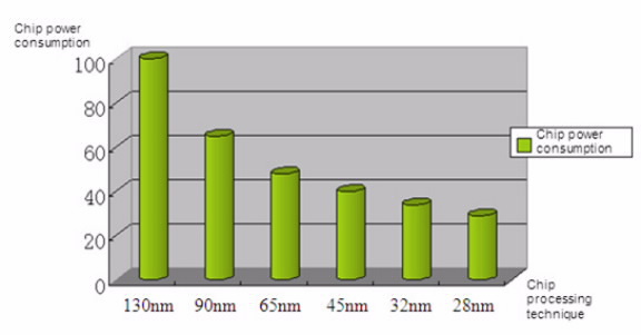
- Cell Leakage power - leakage current. Static component, which depends on the production technology (90/65 / 28nm) and the operating conditions of the circuit (temperature / voltage). The calculated value is proportional to the block area.
- Cell Internal power - current that occurs when the state of the inputs / outputs of the library component changes ( cell - example: logical "or" ORX2, DFF trigger). Dynamic component.
- Net Switching power - the current associated with the recharging of the output capacitance of the component when switching. Dynamic component.
In our example, we got the result that with 26 MHz clocking, our digital processing unit consumes 491 μA in the active mode for 90 nm.
In the next article, we can analyze the consumption of the same IP block when it is implemented in FPGA. For this, each Altera / Xilinx / Microsemi manufacturer has specialized programs within their CAD (Computer Aided Design) systems. In particular, Altera has this part called PowerPlay Power Analysis , which allows you to greatly automate the process described above for its FPGAs . Only here it is well known that the ability to "program" in FPGAany IP-block has a clear negative component in the form of significantly greater consumption. The difference in consumption can reach several tens of times if we compare the implementation of the same IP block in the ASIC 90nm and in the modern FPGA made using 28nm technology .