Using Configurable PIC Microcontroller Logic Cells to Control WS2812
This article is about WS2812b LED control, a little about the synthesis of logic circuits and their implementation inside the microcontroller. An article with small digressions and two bonuses. The first bonus is based on the fact that when we write, we read at the same time (isn't it?). The second bonus will help you start programming microcontrollers and repeat the implementation described in the article in 10 minutes.
The three-color “SPI LEDs” WS2812b (Fig. 1) with the driver and their predecessors WS2811 / WS2812 are connected in series and controlled via a single-wire (serial) bus (hence, they are sometimes mistakenly called “SPI LEDs”, although in this case, especially for “bonus # 1 ”, The SPI interface plays a key role). Each RGB color bit (24 bits, 8 bits per channel) is encoded by a PWM signal (see Fig. 2), with a period of about 1.25 μs. WS2812 LEDs are often used in controlled LED strips and screens, as they have a quick and easy interface, and the number of LEDs is easy to increase. So, for example, at a frequency of 25 frames per second, a video screen can contain one line of (40ms - 50µs) / (0.125µs x 24) ~ = 1300 RGB LEDs. This is not so much, but for advertising signs, a placard or a running line can be quite enough.

Fig. 1. LED strip with digital serial interface

Fig. 2. Coding parameters of the bit sequence.
The use of cheap microcontrollers to generate such short signals (see Fig. 2) presents certain difficulties. So, for example, for a PIC16 controller with a clock frequency of 16 MHz, one command is executed in 250 ns. Thus, to programmatically control the WS2812 driver, you need to spend almost 100% of the kernel speed.
To solve the problem, it would be possible to use the hardware capabilities of the microcontroller, for example, the SPI interface. Such a trick is often used when the sequence “11100000” is transmitted for the transmission of “zero”, and “11111000” for the “unit”, i.e. one bit is encoded byte (or nibble).
Another way is to use the SPI interface and logic elements. The application notes [1] and [2] contain examples on which the described implementation is mainly based.
So, if we take the signals of the SPI interface and invert the SCK signal (synchronization signal) and combine the logical function AND with SDO (output data), then we get the encoded “Units” (Fig. 3).

Fig. 3. The coding of "units"
To encode "Zeros" you need another signal with a shorter duration. To do this, you can use the PWM microcontroller. Zeros are encoded by the signal described by the logical expression n (SDO) * n (SCK) * PWM (n is the inverse). Such an expression is given in [1] and [2], but, as can be seen from the final diagram (Fig. 5), or deduced during the synthesis of the logic circuit using the truth table and Carnot maps, the expression can be written as nSCK * PWM.

Fig. 4. Encoding “Zeros”
It remains to combine the flows of “Zeros” and “Units” with the OR function, and get the desired PWM driver control sequence WS2811 / WS2812.
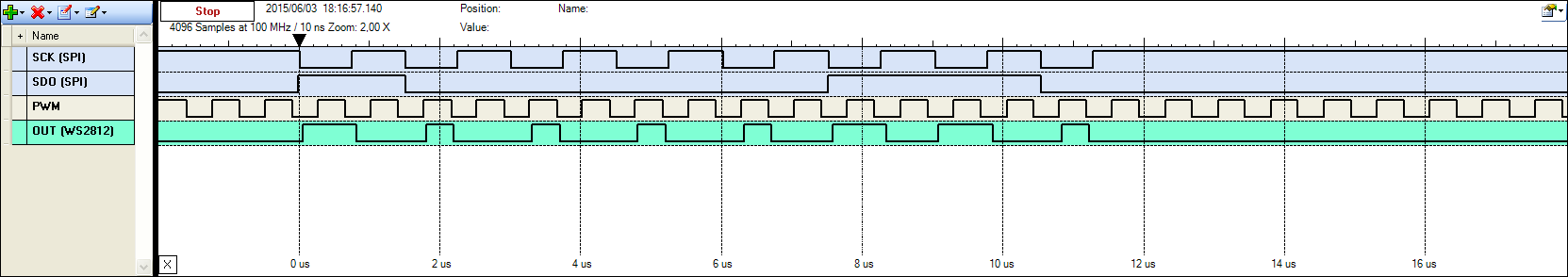
Fig. 5. Stream encoding result.
As a logical expression, the control signal is written as:
(nSCK * SDO) + (nSDO * nSCK * PWM) {1}
Applying the Boolean algebra theorems (see, for example, the wonderful textbook [3]), we can show that the expression {1} is transformed to the equivalent expressions:
n (SCK + nSDO) + n (SDO + SCK + nPWM) {2}
(nSCK * PWM) + (nSCK * SDO) {3}
n (SCK + nPWM) + n (SCK + nSDO) {4}
nSCK * (PWM + SDO) {5}
Many younger Microchip microcontrollers, for example PIC16F1508, PIC16F1509 have built-in Configurable Logic Cells (Configurable Logic Cell, CLC).
Configurable logic cells are peripherals independent of the core, which can help in the implementation of the logically connected operation of the peripherals of the microcontroller and external signals. Asynchronism from the kernel and independence from the program allows you to implement functions that are difficult to implement only programmatically.
The input signals for the CLC can be microcontroller inputs, CLC outputs, other integrated peripheral modules, and internal generators. CLC outputs can be output to ports and shared with other controller peripherals.
Given the above, the combination of the SPI interface and the CLC looks like an ideal option for solving the problem of generating the control signal of the WS2812 LED driver (WS2811).
The CLC Designer utility is intended for visual configuration of CLC and code generation, and the configuration of microcontroller peripherals can also be done through the Mplab Code Configurator (MCC) plug-in to the MPLAB X development environment.
Not all combinations of input signals are present at the inputs of logic cells. Therefore, it is necessary find the combination of signals and cells that are needed to perform a specific task.We need SCK, SDO and PWM signals to encode data on CLC cells.The logic cell CLC4 at its inputs can have signals from SCK, SDO, but it doesn’t have the signal from PWM, and CLC2 can have PWM at its inputs. The output of CLC2 can be connected to the input of CLC4. Therefore, CLC2 will act as a repeater and translate the PWM to the input of CLC4, and CLC4 will perform the logical function of the expressions {1}, {2}, … {5}.

Fig. 6. CLC2 translates the PWM to the output. Gate2 - 4 have log.1 output and do not affect the final result.
In reality, the function {1} in the presented form cannot be implemented on one CLC cell, but its equivalent forms {2} ... {5} are easy. (see fig. 7).

Fig. 7. CLC4 generates PWM encoding of the SPI signal through the function n (SCK + SDA + nPWM) + n (SCK + SDA)
In this case, an additional D-trigger is used, which allows the input signals to be out of sync with respect to the clock frequency of the controller and avoid false switching of the output. In general, for a specific case, the D-trigger may not be necessary, but this configuration gives more predictable timings at the output (synchronization from the FOSC clock frequency).
So, after the configuration of the CLC, PWM and SPI, the preparatory part is over. Now if we write the byte in the SSP1BUF register, then at the output of CLC4 we get the encoded PWM signal in accordance with the WS2812 format. While the SPI module is transmitting data, the microcontroller can perform some other tasks. For each LED, three bytes must be transmitted. The connection diagram is shown in Fig. 8.
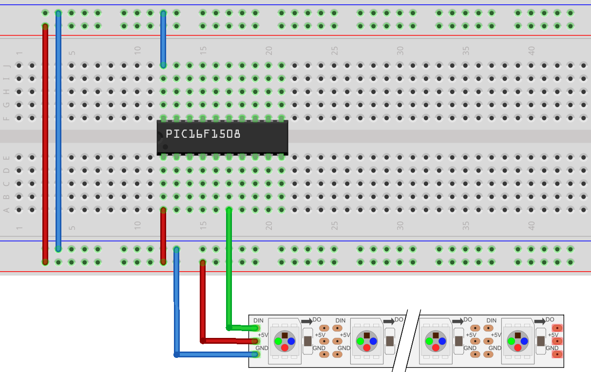
Fig. 8. Connecting the WS2812b tape to the microcontroller
In the described method, the configurable logic and its joint work with the periphery of the microcontroller provide the formation of temporary protocol parameters in the WS2812 format, the program only needs to write the byte to the SPI buffer, the further “magic” is taken over by the configurable logic cells. Since the SPI is used only for recording in the described example, and the SDI input line remains free, an excellent opportunity is provided to use SPI not only for controlling LEDs, but also for receiving external data at the same time. Let's consider how to read data from a memory chip with an SPI interface simultaneously with controlling LEDs.
The microcontroller's PIC SPI port has two shift registers (one for transmission, one for reception) with one address. Writing to SSPBUF starts byte transfer and shifts the bits to the SDO line, but at the same time, data from the SDI input line is shifted to the same register. That is, transmitting a byte to SPI (SDO), we simultaneously receive data from SPI (SDI).

Thus, if WS2812 LEDs and, for example, SPI memory (SRAM 23LC512 or EEPROM 25LCxxx) are connected to the SPI module of the microcontroller, then to transfer data from external memory to the LED strip, the program only needs to transfer data from SSPBUF to SSPBUF, i.e. read a byte from external memory and with the next command send data back to the SPI (LEDs) and at the same time read the next byte, etc.

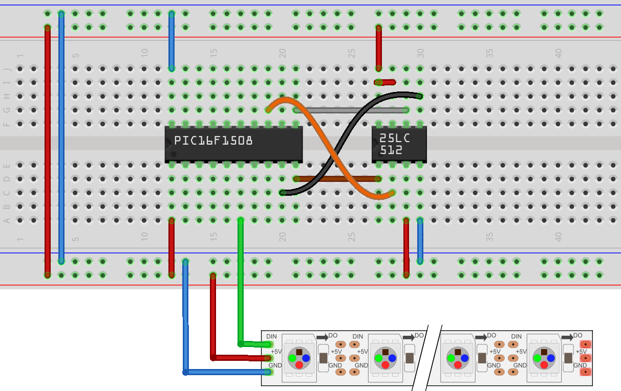
Fig. 9. Connecting external memory
When writing an array of data to external SPI memory or reading the first byte from memory, you need to disable the CLC4 output so as not to give out “garbage” to the LEDs.
Depending on how often it is necessary to update the array of LEDs, the number of LEDs can be very large - it is limited by the update speed and the size of the external memory. From the lines of LEDs, you can create LED screens and displays. The data in the display buffer can be changed while the image is not being updated, this also gives time for more complex calculations, searching in tables, etc., which is necessary to build the displayed image.
The presence of a buffered image in the external memory allows you to display moving images by shifting the start address of the read memory. When using SPI EEPROM memory, pre-recorded images can be displayed. The SPI interface allows you to connect multiple memory chips, for example, one EEPROM for storing character generator, static images, and in the second SRAM create a display buffer for subsequent display on the LED screen.
To study the sources, you can go to the Microchip website (the source code for the AN1890 example is available on the website.
But I suggest watching a short video where in five minutes it’s shown how to do all the magic described above with your own hands.
1. AN1606. Using the Configurable Logic Cell (CLC) to Interface a PIC16F1509 and WS2811. LED Driver www.microchip.com
2. AN1890. Simple SRAM Buffering for Large LED Arrays. www.microchip.com
3. D. Harris, S. Harris. “Digital circuitry and computer architecture” (http://habrahabr.ru/post/259505/)
The three-color “SPI LEDs” WS2812b (Fig. 1) with the driver and their predecessors WS2811 / WS2812 are connected in series and controlled via a single-wire (serial) bus (hence, they are sometimes mistakenly called “SPI LEDs”, although in this case, especially for “bonus # 1 ”, The SPI interface plays a key role). Each RGB color bit (24 bits, 8 bits per channel) is encoded by a PWM signal (see Fig. 2), with a period of about 1.25 μs. WS2812 LEDs are often used in controlled LED strips and screens, as they have a quick and easy interface, and the number of LEDs is easy to increase. So, for example, at a frequency of 25 frames per second, a video screen can contain one line of (40ms - 50µs) / (0.125µs x 24) ~ = 1300 RGB LEDs. This is not so much, but for advertising signs, a placard or a running line can be quite enough.
Fig. 1. LED strip with digital serial interface
Fig. 2. Coding parameters of the bit sequence.
The use of cheap microcontrollers to generate such short signals (see Fig. 2) presents certain difficulties. So, for example, for a PIC16 controller with a clock frequency of 16 MHz, one command is executed in 250 ns. Thus, to programmatically control the WS2812 driver, you need to spend almost 100% of the kernel speed.
Interface Synthesis
To solve the problem, it would be possible to use the hardware capabilities of the microcontroller, for example, the SPI interface. Such a trick is often used when the sequence “11100000” is transmitted for the transmission of “zero”, and “11111000” for the “unit”, i.e. one bit is encoded byte (or nibble).
Another way is to use the SPI interface and logic elements. The application notes [1] and [2] contain examples on which the described implementation is mainly based.
So, if we take the signals of the SPI interface and invert the SCK signal (synchronization signal) and combine the logical function AND with SDO (output data), then we get the encoded “Units” (Fig. 3).
Fig. 3. The coding of "units"
To encode "Zeros" you need another signal with a shorter duration. To do this, you can use the PWM microcontroller. Zeros are encoded by the signal described by the logical expression n (SDO) * n (SCK) * PWM (n is the inverse). Such an expression is given in [1] and [2], but, as can be seen from the final diagram (Fig. 5), or deduced during the synthesis of the logic circuit using the truth table and Carnot maps, the expression can be written as nSCK * PWM.
Fig. 4. Encoding “Zeros”
It remains to combine the flows of “Zeros” and “Units” with the OR function, and get the desired PWM driver control sequence WS2811 / WS2812.
Fig. 5. Stream encoding result.
As a logical expression, the control signal is written as:
(nSCK * SDO) + (nSDO * nSCK * PWM) {1}
Applying the Boolean algebra theorems (see, for example, the wonderful textbook [3]), we can show that the expression {1} is transformed to the equivalent expressions:
n (SCK + nSDO) + n (SDO + SCK + nPWM) {2}
(nSCK * PWM) + (nSCK * SDO) {3}
n (SCK + nPWM) + n (SCK + nSDO) {4}
nSCK * (PWM + SDO) {5}
Many younger Microchip microcontrollers, for example PIC16F1508, PIC16F1509 have built-in Configurable Logic Cells (Configurable Logic Cell, CLC).
Configurable logic cells are peripherals independent of the core, which can help in the implementation of the logically connected operation of the peripherals of the microcontroller and external signals. Asynchronism from the kernel and independence from the program allows you to implement functions that are difficult to implement only programmatically.
The input signals for the CLC can be microcontroller inputs, CLC outputs, other integrated peripheral modules, and internal generators. CLC outputs can be output to ports and shared with other controller peripherals.
Given the above, the combination of the SPI interface and the CLC looks like an ideal option for solving the problem of generating the control signal of the WS2812 LED driver (WS2811).
The CLC Designer utility is intended for visual configuration of CLC and code generation, and the configuration of microcontroller peripherals can also be done through the Mplab Code Configurator (MCC) plug-in to the MPLAB X development environment.
Not all combinations of input signals are present at the inputs of logic cells. Therefore, it is necessary find the combination of signals and cells that are needed to perform a specific task.We need SCK, SDO and PWM signals to encode data on CLC cells.The logic cell CLC4 at its inputs can have signals from SCK, SDO, but it doesn’t have the signal from PWM, and CLC2 can have PWM at its inputs. The output of CLC2 can be connected to the input of CLC4. Therefore, CLC2 will act as a repeater and translate the PWM to the input of CLC4, and CLC4 will perform the logical function of the expressions {1}, {2}, … {5}.
Fig. 6. CLC2 translates the PWM to the output. Gate2 - 4 have log.1 output and do not affect the final result.
In reality, the function {1} in the presented form cannot be implemented on one CLC cell, but its equivalent forms {2} ... {5} are easy. (see fig. 7).
Fig. 7. CLC4 generates PWM encoding of the SPI signal through the function n (SCK + SDA + nPWM) + n (SCK + SDA)
In this case, an additional D-trigger is used, which allows the input signals to be out of sync with respect to the clock frequency of the controller and avoid false switching of the output. In general, for a specific case, the D-trigger may not be necessary, but this configuration gives more predictable timings at the output (synchronization from the FOSC clock frequency).
Digression # 1. Five ways to solve one problem
The implementation of the logical functions {2} ... {5} is shown in Fig. 7a ... 7g. All expressions are equivalent and give the expected result (see Fig. 5).
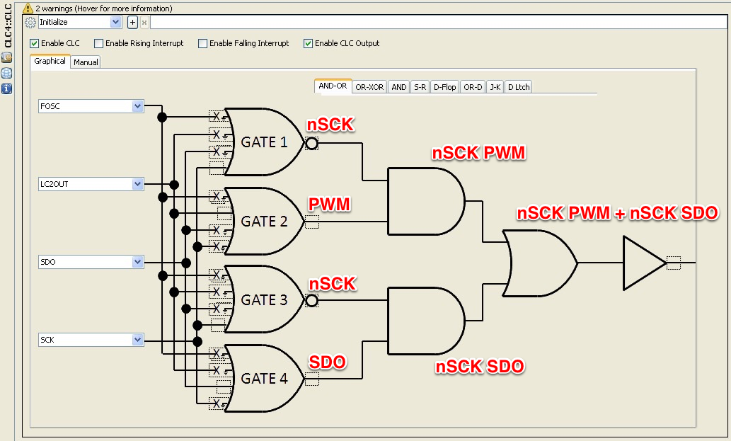
Fig. 7a. (nSCK * PWM) + (nSCK * SDO)

Fig. 7b. n (SCK + nPWM) + n (SCK + nSDO)

Fig. 7c. nSCK * (PWM + SDO)

Fig. 7g n (SCK + SDA + nPWM) + n (SCK + SDA)
Fig. 7a. (nSCK * PWM) + (nSCK * SDO)
Fig. 7b. n (SCK + nPWM) + n (SCK + nSDO)
Fig. 7c. nSCK * (PWM + SDO)
Fig. 7g n (SCK + SDA + nPWM) + n (SCK + SDA)
Digression # 2. Spurious pulses in combinational logic circuits
Situations are possible when a change in the input signal leads to several changes in the output, as a result of which a spurious pulse (glitch) is formed. This can happen if the changing input signal passes to the output in several ways and the number of logic gates traversed in different ways is different. Then, due to the delay of each of the logical elements and the difference in the travel time along the “shortest” and “critical” paths, a spurious impulse can form. This process is well described in [3].
For our specific example, when implementing the functions {1} ... {5} such situations do not arise, but even if they did, the problem can be solved using the OR-D configuration of the configured cells. Then the diagram from Fig. 7d can be redrawn as in Fig. 7 (e), where an additional D-trigger captures the value at the output along the edge of the clock signal of the FOSC controller.
Fig. 7d The same function as in fig. 7g., But with an exit latch
So, after the configuration of the CLC, PWM and SPI, the preparatory part is over. Now if we write the byte in the SSP1BUF register, then at the output of CLC4 we get the encoded PWM signal in accordance with the WS2812 format. While the SPI module is transmitting data, the microcontroller can perform some other tasks. For each LED, three bytes must be transmitted. The connection diagram is shown in Fig. 8.
Fig. 8. Connecting the WS2812b tape to the microcontroller
Bonus # 1. Memory increase
In the described method, the configurable logic and its joint work with the periphery of the microcontroller provide the formation of temporary protocol parameters in the WS2812 format, the program only needs to write the byte to the SPI buffer, the further “magic” is taken over by the configurable logic cells. Since the SPI is used only for recording in the described example, and the SDI input line remains free, an excellent opportunity is provided to use SPI not only for controlling LEDs, but also for receiving external data at the same time. Let's consider how to read data from a memory chip with an SPI interface simultaneously with controlling LEDs.
The microcontroller's PIC SPI port has two shift registers (one for transmission, one for reception) with one address. Writing to SSPBUF starts byte transfer and shifts the bits to the SDO line, but at the same time, data from the SDI input line is shifted to the same register. That is, transmitting a byte to SPI (SDO), we simultaneously receive data from SPI (SDI).
Thus, if WS2812 LEDs and, for example, SPI memory (SRAM 23LC512 or EEPROM 25LCxxx) are connected to the SPI module of the microcontroller, then to transfer data from external memory to the LED strip, the program only needs to transfer data from SSPBUF to SSPBUF, i.e. read a byte from external memory and with the next command send data back to the SPI (LEDs) and at the same time read the next byte, etc.
Fig. 9. Connecting external memory
When writing an array of data to external SPI memory or reading the first byte from memory, you need to disable the CLC4 output so as not to give out “garbage” to the LEDs.
Depending on how often it is necessary to update the array of LEDs, the number of LEDs can be very large - it is limited by the update speed and the size of the external memory. From the lines of LEDs, you can create LED screens and displays. The data in the display buffer can be changed while the image is not being updated, this also gives time for more complex calculations, searching in tables, etc., which is necessary to build the displayed image.
The presence of a buffered image in the external memory allows you to display moving images by shifting the start address of the read memory. When using SPI EEPROM memory, pre-recorded images can be displayed. The SPI interface allows you to connect multiple memory chips, for example, one EEPROM for storing character generator, static images, and in the second SRAM create a display buffer for subsequent display on the LED screen.
Bonus # 2. Do it yourself
To study the sources, you can go to the Microchip website (the source code for the AN1890 example is available on the website.
But I suggest watching a short video where in five minutes it’s shown how to do all the magic described above with your own hands.
Sources
1. AN1606. Using the Configurable Logic Cell (CLC) to Interface a PIC16F1509 and WS2811. LED Driver www.microchip.com
2. AN1890. Simple SRAM Buffering for Large LED Arrays. www.microchip.com
3. D. Harris, S. Harris. “Digital circuitry and computer architecture” (http://habrahabr.ru/post/259505/)