STM32 training for the masses
A little background
I am another graduate of a Moscow university (I will not specify which, but average). Six months ago, we were informed that it was time to write a diploma. At that time, I had just started to master microcontrollers and it was not easy for me, but with a creak that produces a refrigerator when you, alone, try to gently move it without damaging the precious laminate (in my case, linoleum).
My training began when two years ago I became interested in the topic of microcontrollers and an engineer who asked about them gave me a 300x200mm board and said that it has an STM32F217ZGT6 controller and this board has everything you need for training. “In general, if you master it, everything else will seem garbage” (he, however, did not say that to blink the LED, you need to configure SPI, which I did not even hear about at that time). After three not very stressful months of ethereal attempts, recognition of the weakness of programming skills and the huge number of articles I read, I still had to fork out for STM32VLDISCOVERY and the process of copying programs and experiments with them finally went, but still slowly.
For a year and a half I managed to work as a developer, I looked for vacancies where they work with STM32 (since I think that these are the most promising microcontrollers of my class now), I gained experience and when it came to diploma, I remembered my sore calluses. An idea with a theme came instantly: "A debug board on STM32 and a (full-fledged) training course (for the smallest) to it."
Yes, I know, I know, from many engineers I heard that with the topic “debugging board” “if I were a teacher, I would have flunked you on defense”, but still I think any idea has the right to life, so everyone who is interested, please read on.
I am aware that there are many articles that say what, where and how. And how to work with registers, how to understand what they are doing, etc. etc. For me (maybe from a great mind), many of these articles were still not clear and I could not get out of the box by blinking the LED without examples of working code for quite some time. Plus, in even cycles (6-7 pieces) of articles, the system was not always traced, a lot was not chewed (which I really missed), and most importantly, they ended without closing the topic to the end, leaving even more questions.
That is why I wanted to write a complete and complete course, so that others would not be so tormented and figure it out myself. So, having come to the institute and realizing that a quick incentive and understanding is needed (or rather a good pinch), I began to beat myself with my heel in the chest (digging my grave), that I would not only write a training course (in our university I had to call its methodological manual), but I will provide a working layout. They accepted the topic, wrote the assignment (dug the grave, ordered the tombstone), it was a small matter, write and develop everything (lie in the grave, dig in and put the tombstone).
Life has shown that I didn’t have time for half a year at all, but all the time allotted for my diploma was almost over, protection was very soon, but surprisingly, everything was not only ready, but also almost 100% tested (on living people in including).
The output was as follows:
1. The course itself (a scientific guide)
Briefly about it, we can say that in my opinion and according to the reviews of testers, it is full-fledged, but a little harsh and not finalized. Since I decided that I would not write a textbook on programming in SI, therefore, there are no explanations of operators in the course, and therefore they said that the course is harsh in places. As for the incompleteness, I will honestly say that I did not manage to debug everything for surrender, so as to write about it not only here, but also in the methodological manual for the surrender. I also think that it is possible better, but more on that later.
2. Debug board on the STM32F103RET6 controller
Everything is a little better here than in the first paragraph, the board is designed, ordered (due to circumstances, I had to urgently order) in Rezonit, the components are ordered, soldered together (honestly, no video will convey the feeling of the first soldering of LQFP64) and tested (most of it earned immediately). But this is a layout and, of course, there were some overlays: wires, adapters, and various other “crutches,” but unfortunately I won’t have time to order a second revision, but I probably wouldn’t be enough to protect my diploma. So below I will talk in more detail about this debug board.
Arriving at my first job as an electronics developer, I came across one interesting opinion and, as it turned out, it is very common. This opinion sounded something like this: "Here I am a programmer and program microcontrollers, I don’t know circuitry and don’t want to know, by the way, I don’t know how to solder either." Having talked with a group of programmers outside the company, I realized that the person from my work is far from alone in my opinion and although I don’t support him, it’s worth understanding and respecting the opinions of others, all the more it fits perfectly with the then concept of the “everything on board” debug board . In this regard, the board turned out to be quite “greasy”, called STM32SB (SB-StudyBoard) V1.0b. Below we will analyze what went into it.
1. The microcontroller
Based on the fact that I worked with the STM32F103RET6 microcontroller, he was chosen for the project.

2. Power scheme and hardware USB controller
This microcontroller has a built-in USB, which it was decided to put on a separate connector.

3. Speaker
It was decided to introduce for the development of PWM modulation and learning to write melodies.

4. Digital indicator and a shear resistor
For the simultaneous development of a dynamic display and a shift register, it was decided to combine them.

5. LEDs
LEDs, what could be better? Only three-color LEDs on which you can master a smooth color change.

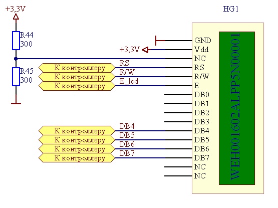
6. LCD display
The standard LCD display is 2 lines of 16 characters each for mastering the parallel interface.
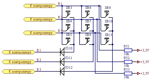
7. Keyboard
Matrix keyboard, you need to know and be able to.
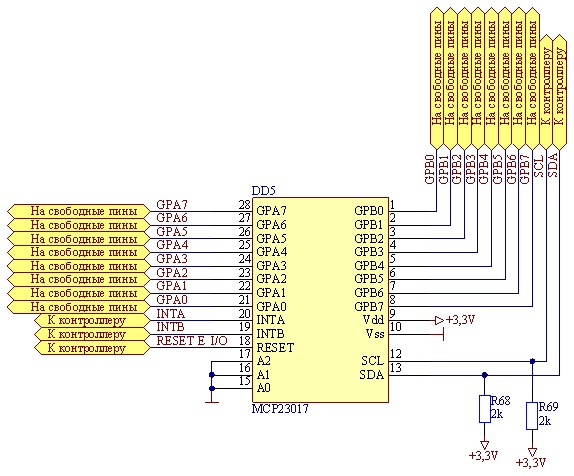
8. I / O
port expander Many I / O ports do not exist, and here I2C can also be mastered.
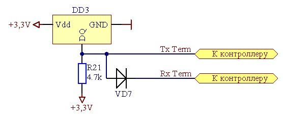
9. Electronic thermometer
1-Wire temperature sensor, a useful thing and valuable experience with it can be useful.
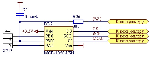
10. Electronic potentiometer.
On this thing you can master a full-fledged SPI and try to take measurements of voltage changes through the ADC.
11. Relay
Although it is at the level of blinking an LED, it’s still nice to hear a familiar click, right?

12. Key transistors
Also at the level of blinking LEDs, but suddenly to whom the principle is not clear.

13. Duplication of free pins on external conclusions
Well, this is a natural design for any debugging board, suddenly everything that is in it was not useful to anyone, but you still need to connect something of your own.

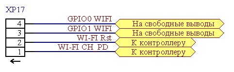
14. WIFI-UART converter (esp8266)
The converter participates in the circuit as a connector, it is also indicated here. The already sensational esp8266 module is used.
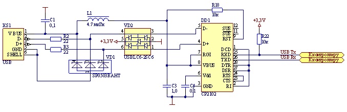
15. USB-UART
USB converter is always cool, CP2102 chip is used here.
16. JTAG and SWD
Well, where do without these things.

Such a wide range of external devices will make it possible to master most of the tricks and try to work with most interfaces without bothering with the purchase of elements and without leaving the table, which is consistent with the concept of not only “everything on board”, but also “for the smallest” (who can’t solder )
Of course, there were some overlays, but, as one familiar engineer says, "the skill of an engineer is measured in the number of tracks cut in the first iteration of the board."
Here is a list of my “jambs”, something that I did not notice, forgot or did not even know when developing this board:
1. I realized that the SWD pins are located in a strange order and this does not interfere with the board. I heard, in my opinion, the correct opinion that they should be positioned as they are located on STM32VLDISCOVERY in order to avoid misunderstandings for the new user.
2. It is not worthwhile to connect single-color LEDs, as on this board, due to the fact that to blink them you need to remove JTAG, but the result was an unexpected effect on me for indicating the firmware loading process.
3. I developed my logo for this board, which I wanted to transfer to the PCB and place on the board, but forgot.
4. To save space in the second revision of the board, I would place some components not used by the user SMD on the bottom side of the board.
5. I realized that for a more convenient wiring of circuits with quartz resonators, it would be convenient to replace them with SMD.
6. I forgot to sign where JTAG and SWD are, they also have not shown how to connect them, and if everything is not so difficult for JTAG and its BH-20 connector, then the situation with SWD is somewhat more dangerous.
7. When developing the footprint of the LCD, an incident came out and the holes were too small for the M3 bolts.
8. The terminals RX and TX are reversed for the CP2102. Since I'm used to the fact that the documentation provides an example of a connection with respect to the microcontroller, and not an external device, I had to cut 2 tracks.
9. On this board, the distance between the pinouts is not standardized by inches, in this connection there is a problem for connecting to the solderless breadboard by sticking it into it.
10. An overlay with current limiting resistors in the relay enable indication circuit came out, the rating was too large for the relay to be switched.
11. Well, as usual, "a good thought comes afterwards." So, after receiving the board, I realized that it was worth making the size suitable for at least some kind of housing - apparently it will have to be finalized in the second revision.
12. Initially, a small digital indicator was laid down, since it did not occupy a large area and was available in stores, but it turned out that in fact it is available everywhere with orders of 520 or more, so I had to sculpt an adapter for a standard digital indicator.
Finally, I will show you a 3D model of this board:
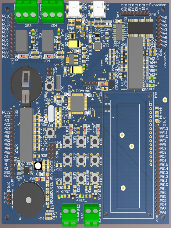
And to compare the photos of it, how it turned out “live”, the view from the top:

And the view from the side, so that more “crutches” could be seen:

Sorry, I would not want to spread the whole project before passing the diploma, but after this work I had a question, is it worth developing this project? I was visited by the idea of writing a series of articles devoted to training, where such a full-fledged course on this debug board would be presented, where everything is written in simple words and explained on the fingers. I would like to hear from you in the comments how much this would be useful and necessary at the moment.
Thanks for attention!