Functional PCB Testing
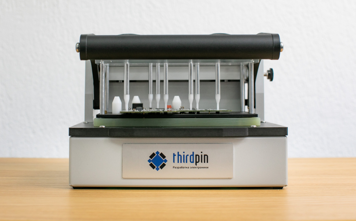
Technological design
DFMs are design and project management principles that aim to successfully produce a finished product. Adherence to these principles is intended to reduce the time for putting into production and the time for testing finished products, while simultaneously improving quality. DFM begins long before the design, at the stage of discussion of technical specifications, depends on the size of the series and affects the cost of design, manufacturing and testing. About DFM wrote on Habré, for example here . Today we will talk about functional testing of the printed circuit board and describe its preparation for this purpose. (traffic)
In the industrial design of printed circuit boards, DFM is provided, including such functions as: DRC (Design Rule Checking) - for checking technological constraints, CAM (Computer Aided Manufacturing) for preparing the production of boards, and DFA (Design For Assembly) for optimizing assembly. These functions can be embedded in CAD software (computer-aided design of printed circuit boards) or delivered as separate software. Here you can note Vayo , in which there are software modules for testing software: DFM Expert (used including for analyzing test sites) and Test Expert (designed to automatically assess product testability and prepare data for electrical testing equipment).
We use Altium Designer (AD) CAD software. It allows you to create control points (CT) as library components, set the rules for placing CT on a diagram and place CT before a trace during topology development. A similar approach can be applied in other modern CAD software.
Electrical contacting methods for testing boards
There are four:
1) Manual
The classic method in which a specialist using hand probes consistently conducts a test of all circuits. Efficiency depends on the skill and personal qualities of the performer.

2) "The bed of the nails"
(From English “bed of nails”, also “contact field”, “needle adapter”, “matrix tester” (MT)). The method assumes the presence of a connecting device with spring-loaded contacts (pogo-pins) opposite the control points on the board. The tester may be part of the production line: Or be a desktop device,

in various mechanical versions:


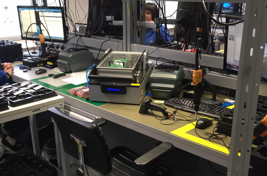


By ensuring that all nodes of the tested software touch the pogo-pins, it is possible to achieve a test coverage level close to 98%.
3) "Flying probes"
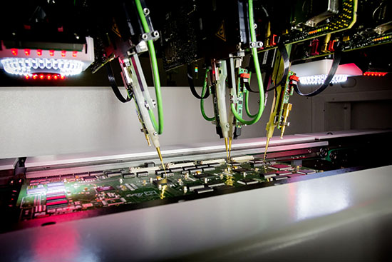
(From the English. "Flying probes"). The equipment for the method of flying probes has several (sometimes several dozen) moving heads, on each of which there is an axis-mounted probe. The probes on the program previously created by the operator are in contact with the board, as a result of which the power supply, signals are supplied and measurements are taken. It is built in line or used separately, depending on the features of the product and the chosen testing methodology. It looks something like this , it sounds like a giant sewing machine.
4) "Flying matrix"
(From the English. "Flying grid", also "flying bed of nails"). A hybrid of the two previous methods, when a matrix of probes is placed on a movable carriage, with each probe may also have an independent drive along the axis. A general idea of how this works can be obtained from the video.
You can read more about the different methods of electrical contacting here .
A number of advantages and disadvantages of the four methods are presented in the table:

Reasons for choosing matrix testing and its features
In real conditions of the Russian reality, the customer has to choose between the first two lines of the table, because the equipment for the last two methods is not cheap (from 15 million rubles for second-hand) and is rarely seen in domestic production. Because of the low cost, preference is usually given to the manual method, in which only the developer himself or a specialist of a comparable level can fully test the product. As a result, products can leave production without any electronic testing at all, or are checked only by switching on “smoke”, and often already on the customer’s side. In better cases, manual testing with the use of tooling is encountered in production, less often - automated testing on matrix stands.

The need for a stand arose in our project Blueberry . This product has four precision analog outputs with individual calibration, so testing it is a laborious task, even for an experienced engineer. We wanted to simplify the process so much so as to eliminate the possibility of human error, reducing the procedure to purely mechanical operations, while ensuring functional testing of each product from an experimental batch (1020 pcs.) Matrix testing was more expensive than manual testing, but this was the only way to ensure proper operation of each devices.
An important factor when choosing a testing method may be the possibility of pre-optimizing the placement of contact pads (in the coordinate grid) on the tested PCB and minimizing their number. Such analysis should be carried out before the beginning of the PCB layout stage, and its goal is to obtain the highest possible level of test coverage.
In our case, this did not work - the board revision was already the 4th when the decision was made, we had to add small contact pads almost to the ready topology.
By reducing the number of pads and pogo-pins, the complexity of software development for functional testing increases. At the same time, the reduction in the number of pogo pins generally reduces the cost of tooling and the time required for its manufacture.
In our case (for 42 pogo-pins and 32 tests), the development required 560 standard hours, of which 200.5 hours took 2 revisions of the hardware, 31 - supply and 328.5 - programming.
In the absence of sufficient space for platforms on the underside of the PCB, for example, with dense two-sided assembly of components, contact pads for testing can also be placed on the upper side of the board. But we must bear in mind that the cost of designing a two-way tester will be 1.5–2 times higher than one-way.
Matrix tester Ingun MA 260 / F
Images of the Ingun MA 260 / F purchasing equipment and the Blueberry circuit board are shown in the figures. Description of the tester can be found here .
 |  |
|---|
The image of the finished device with a cut section: In the drawing we see: 1 - pressure plate, 2 - pressure bar (through it the upper part of the toolbox presses the board), 3 - blueberry test board, 4 - moving panel, 5 - probe board , 6 — testing board, 7 — probe panel, and 8 — pogo pins. To test the Blueberry board, we modified the hardware parts supplied by Ingun as blanks — a pressure plate, a moving panel and a probe panel, and also developed a probe board and a testing board in Altium Designer.

Below is an image of the tested “Blueberry” board (pos.4) relative to the pre-positioning rods (pos.1). POS.3 in this figure is a movable panel, and POS 2 - centering rods (PCB catchers). The installer sets the PP without aiming all the pre-positioning rods (pos.1), then releases the board, and it hits the more accurate centering rods. Without pre-positioning, it is difficult to quickly install the board on the centering rods.
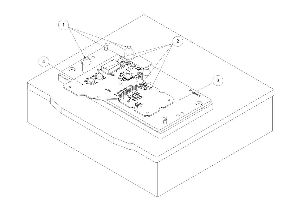
For reliable placement of the PCB on the MT, the board must have at least three holes for the positioning contacts (they are also called pin-on-pin), two of which should be placed diagonally. The diameter of such holes is usually not less than 3.25 mm. The distance from the edge of the positioning contact to the edge of the PCB is at least 3.18 mm, and to the nearest contact pad is at least 5 mm.
Pogo pins must be selected in accordance with the types of control points on the PP and ordered separately (they are not included in the tester package). You can vary the depth of landing pogo-pins for components of non-standard height, but it is desirable to avoid it (by adding additional control points on the PP). The accuracy of hitting pogo-pins in control points (CT) is determined based on the accuracy of the tester and the tolerances of the size and shape of the modified tester boards. The developers of pogo-pins give some recommendations on the size of CT. Also about the choice of CT sizes is well written here .
Used pogo pins (pogopins, spring-loaded contacts)
There are many types of pogo pins for testers that differ in size, shape, and topography of the contact surface (flat, coronated, needle, tapered, etc.), pogo pins material, and coating to ensure their durability. The correct selection of needles with heads corresponding to a specific place of contact ensures high reliability of the contact during testing and the durability of the pogo pins themselves. For ease of replacement, contact probes are usually mounted in holders.
In MT for Bilberry software, Ingun “GKS-100 314 130 A 1500” pogo pins and “KS-100 47 05” pogo pins are used.
Pogo-pin GKS-100: Tip 14 pogo-pin GKS-100: Holder KS-100 for pogo-pin GKS-100: Tip 05 of holder KS-100
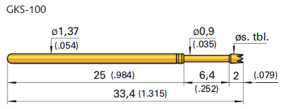


Other pogo pins can be found at the links: Ingun and FEINMETALL .
For different control points on the PP, different types of pogo-pins are used. Control points can be: contact pads (KP) on the surface of the PC with the opening of a protective mask (type KP under the smd-component), through-through metallized holes and pin terminals of the components, soldered into the holes. It is worth noting that a vias can be used as CT, including and masked.
An example of creating a control point in the form of a through hole in the board
Creating a CT as a through hole in AD includes:
1. Creating a circuit element (VGO) in the .schlib library. Often, CT on the diagram is depicted as a socket, and in the standard library MiscellaneousConnectors.schlib there is such a circuit element called Socket. It is enough to copy it into your library, assign a new name to it, change the Default Designator parameter, for example, to KT, and in order for KT not to be included in the list of elements, you must specify the Standard (No BOM) type. 2

A seat (in the .pcblib library) is convenient to create using the Pad command. For the KS-100 pogo-pin in FR-4 fiberglass FR-4 Ingun recommends using a hole with a diameter of 1.7 mm. Consider the example of KP for multilayer PP. The KP size on the testing side (for contact with pin-pin) will be 1.7 + 0.5 = 2.2 (where 0.5 is twice the minimum width of the conductor according to accuracy class 3). We will make a large gearbox from the bottom, taking into account the fact that more often the pin components are located on the upper side of the board, and, accordingly, the pins that are used for testing will be at the bottom. In the remaining layers, the diameter of KP will be 1.9 mm. The hole must be metallized. At the bottom left opposite Assembly Bottom put a tick. 3. Then you need to connect the seat to the circuit element.
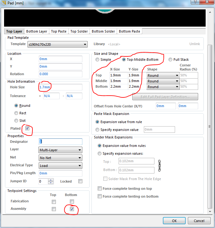
Adding control points in the diagram
In AD, the default is to locate CT on all electrical circuits. But to minimize the number of pogo-pins, CT is installed only on power circuits and on circuits connected to analog and digital external interfaces (except those that can be tested using JTAG). As already mentioned, pogo-pins can come into contact with the gearbox on the surface of the PCB, through the metallized holes and the pin pins of the components, soldered into the holes. At the design stage, it is possible to envisage the use of pin pins of components (soldered into holes), if the pitch of electronic components (EC) housings corresponds to the pogo pin placement step, and all EC with pin pins will be placed on one side (testing side). But it is not always convenient, incl. because of, that the type of case is sometimes chosen (or changed) during the development of the topology. At the design stage of the scheme, it is recommended to lay the maximum number of CT, and then, during the development of the topology, remove excess CT.
To add CT to the scheme using standard methods of placement of UGO. For end-to-end design, we can set design rules in the scheme (for subsequent verification by DRC). It is convenient to set the rules for locating CT for the class of electrical circuits (in which the tested circuits are included). In the diagram, you can create a circuit class using the Place / Directive / Net Classes directive. The directive can be placed on each chain (which must be included in the class), on the bus (but for this, all the tested chains must first be connected to the bus) and on the Blanket. Blanket is a polygonal area (polygon) created using the Place / Directive / Blanket command (select all the chains for the class as a polygon). Installing a directive on the bus is not necessary - just set the Generate Net Classes for Buses option in the Class Generation tab in the project options. Classes are more convenient to create in the PP topology, but in AD there are problems with automatic changes (when updating the schema from the topology) when working with the classes created in the topology, so we create classes in the schema. To create a rule for placing CT in the class properties (in the Net Classes directive), click the Add as Rule button and then the Edit Rule Values button. In the Testpoint category, select Assembly Testpoint Style and click OK. Then set the rules for placement of CT. In the scheme, the set of rules for CT is slightly smaller than in the topology — here you can specify the size of the points, the grid spacing of the test points (with tolerance), the gaps and the placement side. Since we are considering preparing for testing at the design stage, it is better to place the CT in the grid. For KS-100 holders, the documentation contains step 2.54mm. Set Component Body Clearance (the gap between the control point and the body of the component) is equal to 0.8mm, and Board Edge Clearance - 1mm. The remaining gaps do not need to be specified if we place the CT in the grid.
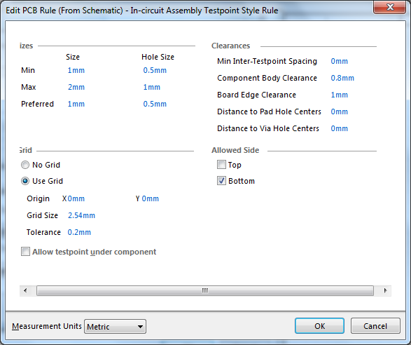
In order for the classes of circuits created in the diagram to be transferred to the software topology, the Generate Net Classes option must be enabled in the Class Generation tab in the project options (it is usually enabled by default).
Placing control points on the board
CT is placed before the trace, but after placing all the other components on the board. Before placing you need to set the grid spacing of CT (in our case 2.54mm).
Before placing the CT, we go into the Design Rules, and there we will see that there are 2 rules in the Assembly Testpoint Style rule set: Schematic Assembly Testpoint Style, which we specified in the scheme for the class, and the default AssemblyTestpoint rule, which applies to all circuits. The default rule we remove. In the settings of the Assembly Testpoint Style rule in the topology there is a difference (from the settings in the diagram) - here the Rule Scope Helper option appears. In our case, you need to add a tick Thru-hole Pads.
It is better to enable checking the placement of CT on-line in Tools / Design Rule Check, in order to immediately control the gaps between the CT and the EC housing, and between the CT and the edge of the PCB. It is necessary to enable online mode for the Assembly Testpoint Style rule.
To control the CT in the topology, it is convenient to use the Testpoint Manager Test Point Manager (in the Tools menu). Description of the interface can be read here .
Analytical data on the performed matrix testing
For testing, we use: a test bench (as part of a single case), a ST-Link / v2 programmer, an external simulator of the control system (output switch), an external control voltmeter, a laboratory power supply, a Windows 10 PC, and a label printer.
The testing algorithm includes:
- system diagnostics,
- obtaining a simulator software version,
- power supply and checking voltage and current consumption,
- serial number firmware,
- serial number lock,
- bootloader firmware,
- getting the software version of the bootloader,
- main program firmware,
- getting the software version of the main program,
- flashing the base calibration tables,
- checking the power supply,
- checking control lines,
- checking on and off load power,
- calibrating phase shifter bias voltages,
- re-flashing calibration tables,
- checking module calibration,
- printing labels.
Conclusion
As a result of testing 1020 “Blueberry” boards, we rejected 77 boards. 44 of them could not fulfill their functions due to inadequate nutrition. As it turned out, the problems were related to the power sources that were supplied in two separate batches. Sources belonging exclusively to one of the batches were installed on all the rejected boards. Our analysis showed that all these sources during at least one test showed unacceptable deviations from the parameters stated by the manufacturer.
Another 33 defects were revealed, including short circuits, poor rations, etc. The total reject rate was 7.55%, which is a good indicator for an experimental batch. The test results of each product are stored in the database, which allows you to quite accurately identify the causes of failures.
The preparation of the draft "Blueberry" for matrix testing was carried out at the final stage of the topology development, which created difficulties when adding contact pads. The size of the KP was chosen insufficient (1x1mm), as a result there were problems with contacting when the pogo pins fell past the KP. The share of such failures is insignificant.
In our next project using matrix testing, we laid the CT in advance. Now you can connect to the stand database remotely. The firmware of the stand has protection and maintains profiles with different levels of access to the settings, so the stand can be placed on a remote contract manufacturing, which we successfully did in Kaliningrad. But more about that in a separate article.

