Thermal barriers, tombstones and other charms of printed circuit boards
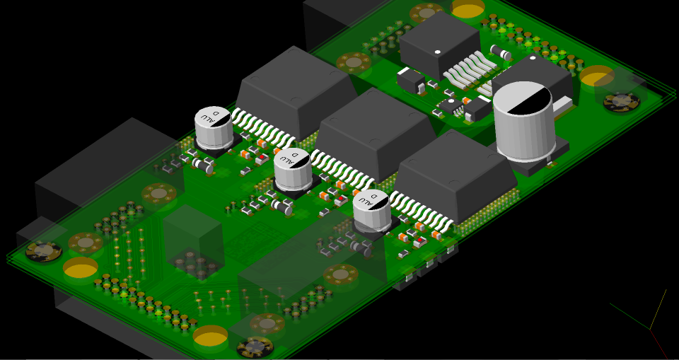
While cool designers are designing the right circuit boards and ordering production at state-of-the-art American-European plants, let us turn to the experience of developing printed circuit boards for the urgent production of one of the Moscow region (in fact Zelenograd is a district of Moscow) plants with manual basement installation (in fact, manual installers at they sit already on the second floor, and in the basement there is a line of 60,000 components per hour).
Further text is the personal opinion of the author. This is not the ultimate truth, but only one of the possible sections of the huge layer of information that is currently available to the ordinary designer.
Let's talk a little about CAD. Despite the fact that there are a lot of them, almost all of them provide the designer with approximately the same basic functionality. Having the necessary knowledge, you can also make a high-speed differential pair in Sprint-Layout (no offense!), Which will work fine. The only question is how long will the trace of this pair take. At the same time, you can screw up in the same PADS in such a way ("working with tracing" from the electronics is full of examples of interesting designs) that you will have to disentangle for a long and tedious:

What is it for? And to the fact that if the designer is an idiot, then no ultra-modern CAD will solve the design problems for him. Yes, there will be a check of all kinds of rules and much more. But to consider absolutely everything is impossible. This is especially true for issues of soldering and installation (although with checking placement recently it’s getting better and better).
Unfortunately, when designing software, there are often completely mutually exclusive paragraphs. A typical example is power blocking capacitors. On the one hand, you need to place them as close as possible to the power output of the chip.

On the other hand, it is impossible to put the components close to each other if it is planned to automatically install (who knows, what are the limitations of a particular machine that will arrange the components) and reflow soldering (the capacitor may be in the so-called “shadow” of the high component, and if heating the paste on its pads will not melt, as it should).
And we must not forget about the frequencies at which everything works for us, and how the inductance of the paths from \ to the capacitor will affect its properties in a particular circuit (I strongly recommend reading this and this for a better understanding of the issue).
But back to our stones and barriers. If you don’t know what to do, then what should you do? Read the documentation, of course! And she is, and a lot!
We will not touch our GOSTs, some of which have not been updated for more than forty years. Let us turn our attention to IPC standards, which are used by a large (unjustified personal opinion of the author, because I do not know the exact numbers) part of PP designers around the world. The standards tree shows that first of all, you can read something from 2220 and 7351. Of the 2220, we are primarily interested in 2221 - Generic Standard on Printed Board Design . The previous version of the standard is by reference, since the current version is only for money (well, we know that everything can be found if desired). In particular, about thermal barriers is written in section 9.1.3. If we briefly translate what is written there, then it comes down to the fact that if the output component (and 2221 is devoted exclusively to output components), then

It is advisable to make thermal barriers, since their presence facilitates soldering.
Let's now see what a thermal barrier is: And what does it help in? Well, firstly, when soldering a wave. This type of soldering is mainly used in very large-scale production. At the same time, there are a number of restrictions on the placement of components for the solder wave and a bunch of recommendations on the landing sites for the components. Dave, as always, simply and clearly explains what’s what:


Optimization, in a word, in order to reduce the amount of marriage.
Interesting process:
The problem here is that not all cars have a pre-heating zone, and it does not always help if the polygons are large. It turns out that if you drive the board more slowly, so that large polygons are warmed up, then there is a great chance of overheating small components. Thermal barriers help solve this problem. But the devil is in the details, as always.
Before moving on, let's talk a little more about manual , rather than machine soldering.
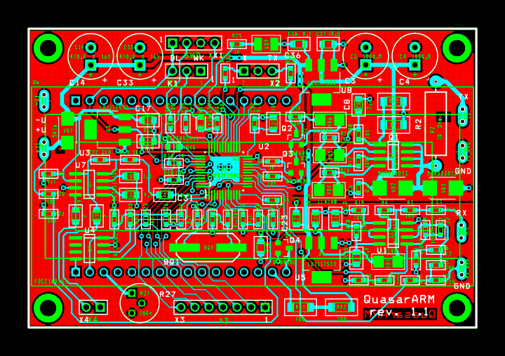
Imagine that you have a multilayer board, as on the cdpv at the beginning of the article, and you need to solder the connectors into it. But some problem is that the board is six-layer, and four layers are stupidly ground for the entire board. And half of the pins in the connectors are ground. You can, of course, take advantage of preheating to 100-110 degrees and then solder. But this is not always possible. Yes, and I do not want to warm the tantalums once again (after all, all the small things were soldered first, and the connectors last). This is where thermal barriers help. The soldering iron heats only the output of the connector, the metallization glass and the contact spots, and not all the polygons in all layers.
And here the problems begin.
It is obvious that the thermal barrier reduces the total area of copper through which the component and the polygon come into contact. That is, the physical resistance of the contact increases. The parasitic inductance of the compound also increases.
A fairly cursory search showed that there are at least three articles in which the question of resistance, inductance and the relationship of all this is studied.
Here they are:
- A Demystifying Study of Thermal Relief Pads: Tradeoff between Manufacturing and Cooling
- Investigation on the Efficiency of Thermal Relief Shapes on Different Printed Circuit Boards
- Modeling the Low- and High-Frequency Impedance of Thermal Reliefs
All articles are published by IEEE , which suggests that there is no outright nonsense.
Again, I highly recommend that you familiarize yourself.
The conclusions of all articles, in short: yes, thermal barriers are cool and useful, but you need to use them wisely (who would doubt it, right?). If in doubt, at least it is necessary to stimulate. Basically, this all applies to components for surface mounting, since the output components already have sufficient parasitic inductance of the terminals.
As for the resistance, yes, it increases slightly at the point of contact. About a unit milliom. If this is not critical, then you can use it. And, of course, it is necessary to take into account the current that will flow through this connection. If it is such that there will be heating, then you should look at what is more important: some local overheating or ease of installation.
For myself, I deduced such a rule. Thermal barriers can be safely used on mock-ups, because all the same, mock-ups are mainly soldered manually. On serial products, you should consult with specific production where the boards will be mounted (it is generally useful to do this, in the sense of consulting production), since the technologist knows his assembly line and its capabilities better than you.
But all this concerned output components. But what about surface mount? And here it’s still a bit more complicated. The 7351 Generic Requirements for Surface Mount Design and Land Pattern Standard does not mention thermal barriers at all.
There is an interesting document in which the author advises against using thermal barriers due to the increased impedance of the connection. Indeed, this makes sense: when designing power supplies and other power circuits.
A little distraction.
Hopefully the component placeer looks like many are introducing it.
If not, here is a good illustration of the process:
After stuffing the board, it goes down the conveyor to the reflow soldering oven.
It looks something like this:
Unfortunately, sometimes this effect is possible:
There may be several reasons for its occurrence (you can familiarize yourself with the main ones, for example, here ).
One of them is the curve of thermal soldering profile . The following are (not in order of importance): expired (or improperly stored) paste, improper stencil for transferring the paste, crookedly designed component landing sites, and placeer's errors.
If the thermal profile, paste, placeer and sometimes a stencil is a headache of production, then the curves of the site are the direct jamb of the designer.
The main idea is that the pads should be of the same geometry, so that when spreading the paste, the same surface tension forces arise. Indeed, the rise of the component arises precisely because of the various surface tension forces that act on the planar component. It also happens that the site is very large in itself (connecting to an earthen landfill, for example), there is no thermal barrier, and with a curved thermal profile, the site will warm up more slowly than the other output. As a result, the paste will quickly melt in a non-polygonal area, and the component may stand up.
Nice illustration and related article :
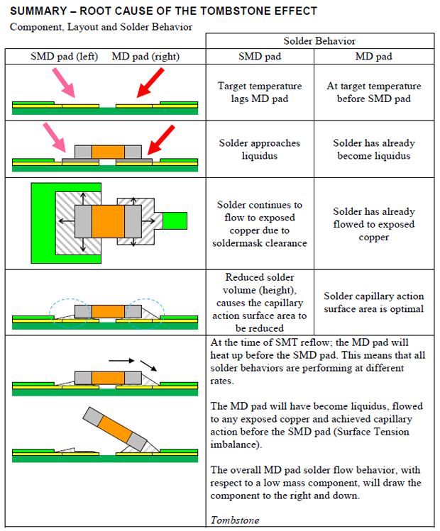
Why did the component stand up? Because even if the cutout in the stencil for the paste was the same on both sites, then in the process of melting the paste at that conclusion, where there is a large area open from the soldering mask, not only heating is slower, but the paste spreads over a larger area, which in the general case greatly degrades the characteristics of the solder joint (insufficient amount of solder) and can lead to the rotation of the component relative to the landing pad.
One office near Moscow, in the sense of Moscow, offers a compromise option: If there is a need for a large polygon open from the mask so that the paste does not spread over the polygon, you can make a locking bridge from the mask of a small width, which will prevent the solder from spreading during reflow.

All of the above mainly applies to lightweight components with sizes less than 0603 (in inches), although there are exceptions.
What is the bottom line?
Thermal barriers are definitely needed. Apply them wherever needed and not necessary - not worth it. This is especially true for microwave technology. In the everyday design of simple microcontroller projects, in my opinion, they do more good than harm. But much depends on the soldering technology and the subsequent need for maintainability of the product.
When soldering in a furnace, one should remember about the possibility of lifting components due to improper design of the landing sites and the jambs of the technologist serving the line.
In any case, when tracing the circuit board, first of all, turn on the brain and analyze!
Thank you for reading!
I ask you to inform about all the errors noticed in PM.
Only registered users can participate in the survey. Please come in.
The author to continue to write about the development of iron?
- 96.5% Definitely yes 1283
- 0.8% Definitely not 11
- 2.6% My eyes would not see you 35