Two bits per transistor: Intel 8087 floating point high density ROM
- Transfer
Intel developed the 8087 chip in 1980 in order to improve PC performance with 8086/8088 processor lines (such as the IBM PC) when performing floating point operations. Since the first microprocessors were designed to perform operations with integers, the execution of operations with floating-point numbers was slow, which already speak of performing transcendental operations, such as trigonometric functions or logarithms. The 8087 coprocessor significantly increased the speed of performing tasks with a floating point, everything was performed almost 100 times faster. The 8087 architecture was also implemented in later Intel processors, and the 8087 instructions are still used in modern x86 PCs. Intel introduced the 8087 chip in 1980, designed to improve the performance of floating-point computing on the 8086 and 8088 processors.
Since early microprocessors only worked with integers, floating-point arithmetic was slow, and transcendental operations, such as triggers or logarithms, looked even worse. Adding the math coprocessor 8087 to the system made it possible to speed up floating-point operations 100 times. The 8087 architecture has become part of the later Intel processors, and the 8087 instructions (although outdated) are still part of modern x86 desktops.
The 8087 chip provided fast floating point arithmetic for the original IBM PC and became part of the x86 architecture used today. One of the unusual features of the 8087 is a multi-level ROM (read only memory) capable of storing two bits per transistor, which is twice the density of a regular ROM. Instead of storing binary data, each cell in the 8087 ROM stored one of four different values, which were then decoded into two bits. Since 8087 needed a large amount of ROM for microcode (1), and the number of transistors on a chip was very limited, Intel used unusual technology to solve the problem. In this article, I will explain how Intel implemented this multi-level ROM.
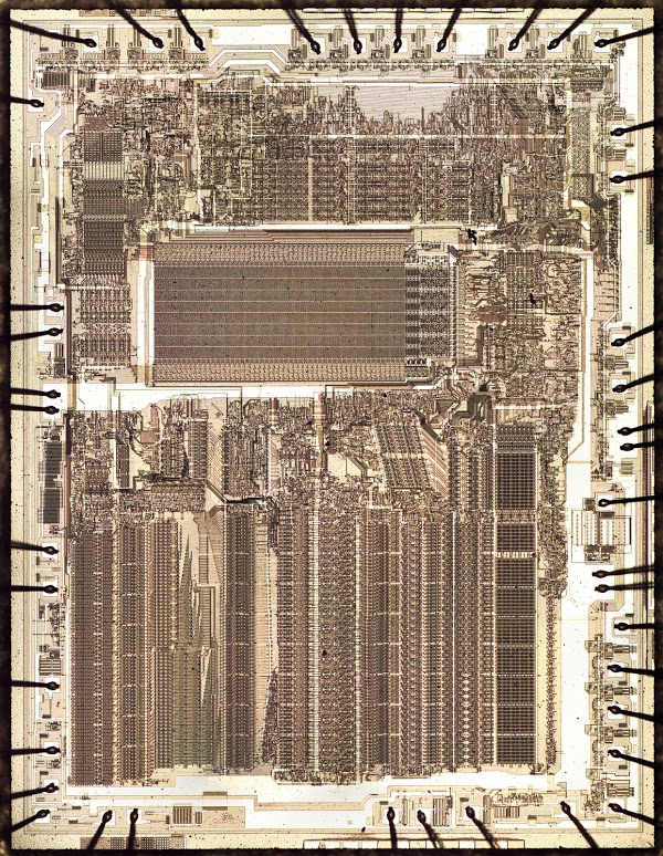
I opened the 8087 chip and photographed it with a microscope, taking a photo below. In the photo I indicated the main functional blocks, based on my own reverse engineering (Click to enlarge image). The matrix of the 8087 processor is quite complicated, with 40,000 transistors (2). 8087 uses 80-bit floating-point numbers: 64 bits are reserved for the mantissa, 15 bits for the exponent, and another sign bit. (An example of a number with a base of 10: in the number 6.02 × 10²³ 6.02 is the mantissa, and 23 is the exponent). At the bottom of the photo, the word “fraction processing” marked part of the scheme for the mantissa. From left to right, this includes: a constant store, a 64-bit offset, a 64-bit adder / subtractor, and a stack of registers. Slightly above is the circuit for handling exponentials.
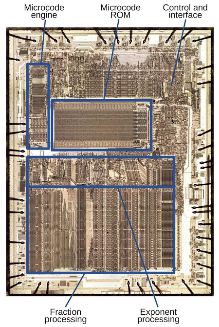
Matrix coprocessor chip for floating point operations Intel 8087, with the designation of the main functional blocks. The
execution of the 8087 instruction required several steps, and in some cases more than 1000. The microprogram 8087 used microcode to determine low-level operations at each step: shifts, increment, memory samples , reading constants, etc. You can perceive microcode as a simple program written in the form of microinstructions, in which each microinstruction generates control signals for various components of chi na In the photo above, you can see the ROM with the microcode program 8087. The ROM occupies most of the chip, clearly showing why a compact multi-level ROM was necessary. To the left of the ROM is the “engine” on which the microcode program was run, in fact, a simple processor.
8087 worked as a coprocessor with an 8086 processor. When the 8086 detected a special floating point instruction, the processor ignored it and allowed the 8087 to execute the instruction in parallel. I will not explain in detail the internal work of 8087, but, briefly, floating point operations were implemented using integer addition / subtraction and shift operations. To add or subtract two floating point numbers, 8087 performed a bitwise offset of the number until the binary separators (that is, the decimal separator is a comma, but in the binary system) are matched, and then added or subtracted the mantissa. Multiplication, division and square root were performed by multiple shifts, additions or subtractions. Transcendental operations (tan, arctan, log, power) used the algorithms CORDIC, which use shifts and add special constants, processing one bit at a time. 8087 also encountered many particular cases: infinity, overflow, NaN (not a number), denormalized numbers and several rounding modes. The microcode stored in the ROM controlled all these operations.
Chip 8087 consists of a tiny silicon matrix, on which silicon is doped with impurities in places in order to obtain the desired semiconductor properties. Polysilicon (a special type of silicon) that forms wires and transistors is deposited on the silicon surface. And finally, the metal layer on top of the silicone completes the working electrical circuit. The photo below, on the left side shows a small part of the chip, as it is visible under the microscope, showing a yellowish metal wiring. On the right side of the photo, the metal was removed with acid, exposing polysilicon and silicon. When polysilicon crosses silicon, a transistor is formed. The pink areas are doped silicon, and the thin vertical lines are polysilicon. Small circles are the contacts between the silicon and metal layers connecting them together.
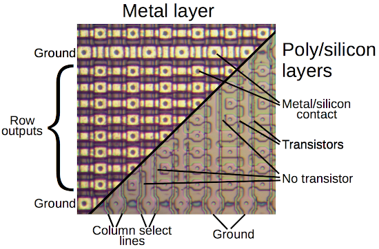
ROM structure in Intel 8087 FPU. The metallic layer is shown on the left and polysilicon and silicon on the right.
Although there are many ways to build ROMs, the standard way is to create a grid of "cells", where each cell stores one bit. Each cell can have a transistor (which means 0 bits) or not have a transistor, which means 1 bit. In the image above, you can see a grid of cells with transistors (where polysilicon is deposited on silicon) and missing transistors (where there are gaps in silicon). To read information from the ROM, one column selection line is activated (based on the address) to select the bits stored in this column and to get one bit from each row at the output. You can see the vertical column selection lines (column select lines) from polysilicon, and the horizontal metal rows in the photo above. Vertical doped silicon lines are grounded.
The diagram below (corresponding to the 4 × 4 ROM segment) explains how the ROM functions. Each cell either has a transistor (black), or does not have a transistor (highlighted in gray). When voltage is applied to the column selection line of polysilicon, the transistors in this column turn on and ground the corresponding metal rows. (in this case, the NMOS transistor is similar to a gate that is open if the input is 0, and is closed if the input is 1.) The metal “rows” of the circuit output the data stored in the selected “column”.
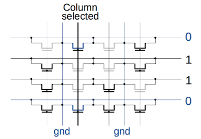
4x4 ROM Segment Circuit
Column selection signals are generated by a decoder circuit. Since this circuit is built from NOR valves, I will first explain the design of the valves. The diagram below shows a four-input NOR gate built from four transistors and a pull-up resistor (although in fact, a special transistor performs the function of a resistor). On the left side of the circuit, all inputs are 0, so all transistors are turned off, and the pull-up resistor keeps the output signal at a high level. In the right part, one of the inputs was fed 1, turning on the transistor. The transistor is grounded, so the output signal is now "low" level. Thus, if any inputs are high (1), the output is low (0). So this circuit implements the NOR valve.
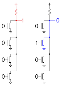
4-input NOR gate built from NMOS transistors
The column selection decoder circuit accepts incoming address bits and activates the corresponding selection string. The decoder contains an 8-input NOR gate for each column, that is, one NOR gate for each address. The photo shows two NOR elements that generate column selection signals (for simplicity, I will show only four of the 8 inputs). Each column uses a different combination of address lines and augmented address lines as input, choosing a different address. Address lines are in the metal layer, which is removed in the photo below; address lines are highlighted in green. To determine the address associated with a column, look at the square contacts associated with each transistor and note which address lines are connected. If all the address lines connected to the column transistors are at a low (0) level,
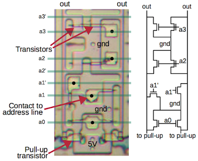
Part of the address decoder. Address decoder selects odd columns in ROM, counting from right to left. The numbers in the upper part show the address associated with each output.
The photo below shows a small part of the ROM decoder with all 8 inputs for NOR gates. You can read binary addresses by carefully examining the connections in the address bar. Note the binary pattern: connections a1 change values in each column, connections a2 alternate every two columns, connections a3 every four columns, and so on. D. Connection a0 is fixed because this decoder scheme chooses odd columns; A similar ROM scheme selects even-numbered addresses (this separation was necessary for the decoder to fit on the chip, since each column of the decoder is twice as wide as the ROM cell).
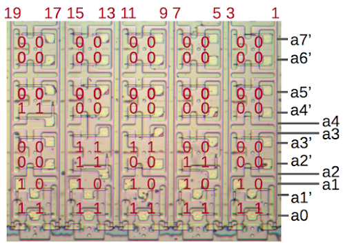
Part of the address decoder for ROM 8087 microcode. The decoder converts an 8-bit address into column selection signals
The last component of the ROM is a set of multiplexers, which reduces 64 output lines to 8 lines. Each 8-to-1 multiplexer selects one of its 8 inputs based on the address. The diagram below shows one of the 8087 processor row multiplexers, built of eight large pass-through transistors, each of which is connected to one of the “row” lines. All transistors are connected to the output so when the selected transistor is turned on, it transmits its input to the output. Multiplexer transistors are much, much larger than transistors in ROM to reduce ROM signal distortion. A decoder (similar to the one discussed earlier, but smaller) generates eight multiplexer control lines from three address lines.
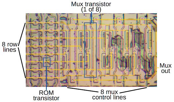
One of the 8-row multiplexers in ROM. Here you can see layers of (poly) silicon, with metallic compounds painted in orange.
Summing up, the ROM stores the bits in a grid. It uses eight address bits to select a column in the grid. Then the three bits of the address select the desired eight outputs from the “strings”.
So far I have explained the typical ROM device that stores one bit per cell. So how could the 8087 store two bits per cell? If you look carefully, the microcode ROM 8087 contains four different sizes of transistors - if we assume the absence of the transistor as one of the sizes (6). With four options for each transistor, one cell can encode two bits, roughly doubling the density (7). The current section explains how the four sizes of transistors generate four different currents, and how analog and digital IC circuits convert these currents to two bits.
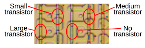
A micrograph of the ROM 8087 microcode shows four different transistor sizes. This allows the ROM to store two bits per cell.
The transistor size adjusts the current through the transistor (8). An important geometrical factor is the different width of silicon (pink), where it intersects with polysilicon (vertical lines), creating transistors with different gate widths. Since the gate width controls the current through the transistor, the four transistor sizes generate four different currents: the largest transistor passes most of the current, and the current does not flow at all if there is no transistor.
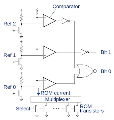
The ROM current is converted to bits in several steps. First, the pull-up resistor converts the current to voltage. The three comparators then compare the voltage with the reference voltage to generate digital signals, determining which voltage is higher / lower. Finally, logic gates convert the comparator's output signals to two output bits. This scheme is repeated eight times, generating a total of 16 bits on the output.
The circuit for reading two bits from the ROM cell
The circuit above performs these conversion steps. As a result, one of the ROM transistors is selected by the “column” selection line and the multiplexer (discussed earlier), which generates one of the four currents. Then, the pull-up resistor (12) converts the current of the transistor to voltage, with the result that the voltage depends on the size of the selected transistor. Comparators compare this voltage with three reference voltages, and output 1 if the ROM voltage is higher than the reference voltage. Comparators and reference voltages require careful design, since ROM voltages can differ by as little as 200 mV.
The reference voltages are midway between the expected values of the voltage of the ROM, which allows for some voltage fluctuations. The “low” voltage of the ROM is lower than all the reference voltages, so all the comparators will output 0. The second voltage of the ROM is higher than Ref 0, so the lower comparator outputs 1. With the third voltage ROM, the lower two comparators output 1, and at the maximum the voltage of the ROM at the output of all three Comparators 1. Thus, the three comparators give four different output patterns, depending on the transistor ROM. Then the logic elements convert the comparator output into two output bits (10).
The design of the comparator is interesting because it is a bridge between the analog and digital worlds, producing 1 or 0 if the voltage of the ROM is higher or lower than the reference voltage. Each comparator contains a differential amplifier that amplifies the difference between the voltage of the ROM and the reference voltage. The output of the differential amplifier drives a gate, which stabilizes the output and converts it to a logic level signal. The differential amplifier (below) is a standard analog circuit. The current source (symbol below) provides a constant current. If one of the transistors has a higher input voltage than the other, most of the current passes through that transistor. The voltage drop across the resistors will cause the corresponding output to be lower, and the other output to be higher.
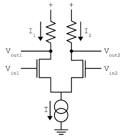
Diagram showing the operation of the differential pair. Most of the current will flow through a transistor with a higher input voltage, resulting in a lower output signal. The symbol of a double circle at the bottom - a source of DC I
The photo below shows one of the comparators on the chip; metal layer on top, transistors under it. I will consider only the highlights of this complex scheme; See note 12 for details. The signal from the ROM and multiplexer comes on the left. Pull-up circuit 12 converts current to voltage. Two large differential amplifier transistors compare the ROM voltage to the reference voltage (input from the top). The outputs from the differential amplifier go to the gate circuit (scattered over the photo); shutter output is in the lower right corner. The current source of the differential amplifier and pull-up resistors are made of depletion-mode transistors. Each output circuit uses three comparators, giving a total of 24 comparators.
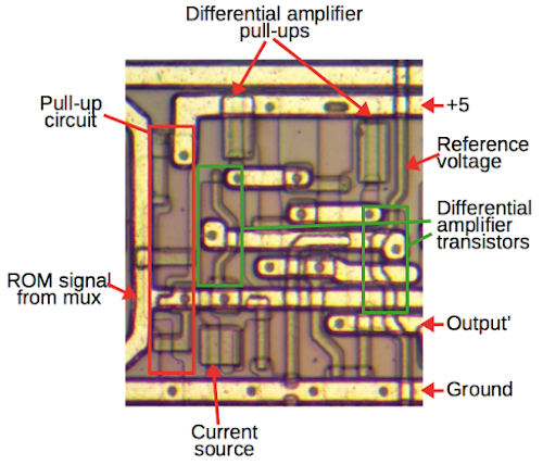
One of the comparators in 8087. The chip contains 24 comparators for converting voltage levels from a multi-level ROM to binary data.
Each reference voltage is generated by a carefully sized transistor and a pull-up circuit. The voltage reference circuit is designed to be as similar as possible to the ROM signal circuit, so that any changes in chip production will affect both elements in the same way. The reference voltage and the ROM signal use the same load circuit. In addition, each reference voltage circuit includes a very large transistor, identical to the multiplexer transistor, although there is no multiplexing in the reference signal circuit — just to ensure “matching” of the circuits. The three voltage reference circuits are identical, except for the size of the reference transistor (9).
A circuit that generates three reference voltages. The size of the reference transistors - between the size of the transistors ROM. The oxide layer was not completely removed from this part of the matrix, which caused color twists in the photo.
To assemble the entire puzzle, the photo below shows the location of the components of the microcode ROM on the chip (12). The main part of the circuit ROM are transistors that store data. The column decoder circuit is located above and below the ROM data. Half of the column selection decoders are at the top, and half at the bottom, for better layout. The output circuit is on the right. Eight multiplexers reduce 64 lines to eight lines. Then eight lines enter the comparators, generating 16 bits at the output of the ROM on the right. The reference circuit above the comparators generates three reference voltages. At the bottom right, a small string decoder controls the multiplexers.
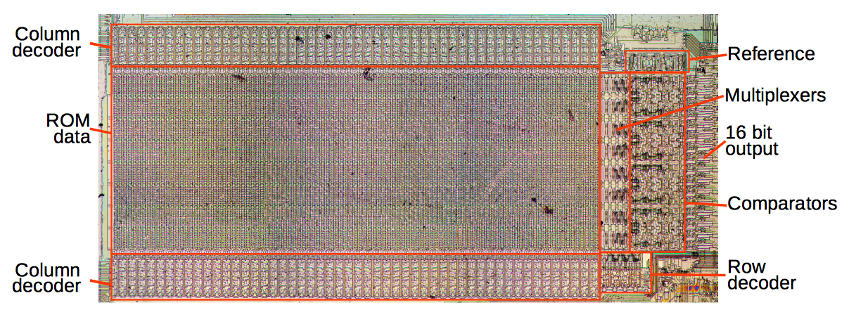
Intel's 8087 FPU microcode ROM with the main component labeling.
Although it may initially appear that a multi-level ROM will be half the size of a regular ROM, the effect is not so noticeable due to the additional comparators scheme, and because of the transistors -for the need to use several sizes. Despite this, a multi-level ROM saved about 40% of the space that would have occupied the usual ROM.
Now that I understand the structure of the ROM, I can simply (but tiringly) read the contents of the ROM, just by looking at the size of each transistor under a microscope. But, without knowing the set of microcode instructions, the contents of the ROM is useless.
The 8087 floating-point math coprocessor used an unusual “two bits per cell” structure to place microcode on the chip. Intel reused the multi-level ROM structure in 1981 in the doomed iAPX system. 432.11 As far as I can tell, interest in multi-level cell ROMs reached its peak in the 1980s and then waned. Probably due to the fact that, according to Moore's law, it is much easier to increase the capacity of the ROM by reducing the standard cell than designing non-standard ROMs that require special analog circuits built with high tolerances (14).
Surprisingly, the multi-level concept has recently returned, but already on flash memory. Many flash devices store two or more bits per cell (13). Flash memory has even reached a remarkable 4 bits per cell (requiring 16 different voltage levels) in consumer products recently announced (QLC, quad-level cell). Thus, the little-known technologies of the 1980s can come back again decades later.
I report my latest blog posts on Twitter, so subscribe to @kenshirriff to read future articles on 8087. I also have an RSS feed. Thanks to Jeff Epler for offering to explore the 8087 ROM.
Thank you for staying with us. Do you like our articles? Want to see more interesting materials? Support us by placing an order or recommending to friends, 30% discount for Habr's users on a unique analogue of the entry-level servers that we invented for you: The whole truth about VPS (KVM) E5-2650 v4 (6 Cores) 10GB DDR4 240GB SSD 1Gbps from $ 20 or how to share the server? (Options are available with RAID1 and RAID10, up to 24 cores and up to 40GB DDR4).
VPS (KVM) E5-2650 v4 (6 Cores) 10GB DDR4 240GB SSD 1Gbps until January 1 for free if you pay for a period of six months, you can order here .
Dell R730xd 2 times cheaper? Only we have 2 x Intel Dodeca-Core Xeon E5-2650v4 128GB DDR4 6x480GB SSD 1Gbps 100 TV from $ 249in the Netherlands and the USA! Read about How to build an infrastructure building. class c using servers Dell R730xd E5-2650 v4 worth 9000 euros for a penny?
Since early microprocessors only worked with integers, floating-point arithmetic was slow, and transcendental operations, such as triggers or logarithms, looked even worse. Adding the math coprocessor 8087 to the system made it possible to speed up floating-point operations 100 times. The 8087 architecture has become part of the later Intel processors, and the 8087 instructions (although outdated) are still part of modern x86 desktops.
The 8087 chip provided fast floating point arithmetic for the original IBM PC and became part of the x86 architecture used today. One of the unusual features of the 8087 is a multi-level ROM (read only memory) capable of storing two bits per transistor, which is twice the density of a regular ROM. Instead of storing binary data, each cell in the 8087 ROM stored one of four different values, which were then decoded into two bits. Since 8087 needed a large amount of ROM for microcode (1), and the number of transistors on a chip was very limited, Intel used unusual technology to solve the problem. In this article, I will explain how Intel implemented this multi-level ROM.
I opened the 8087 chip and photographed it with a microscope, taking a photo below. In the photo I indicated the main functional blocks, based on my own reverse engineering (Click to enlarge image). The matrix of the 8087 processor is quite complicated, with 40,000 transistors (2). 8087 uses 80-bit floating-point numbers: 64 bits are reserved for the mantissa, 15 bits for the exponent, and another sign bit. (An example of a number with a base of 10: in the number 6.02 × 10²³ 6.02 is the mantissa, and 23 is the exponent). At the bottom of the photo, the word “fraction processing” marked part of the scheme for the mantissa. From left to right, this includes: a constant store, a 64-bit offset, a 64-bit adder / subtractor, and a stack of registers. Slightly above is the circuit for handling exponentials.
Matrix coprocessor chip for floating point operations Intel 8087, with the designation of the main functional blocks. The
execution of the 8087 instruction required several steps, and in some cases more than 1000. The microprogram 8087 used microcode to determine low-level operations at each step: shifts, increment, memory samples , reading constants, etc. You can perceive microcode as a simple program written in the form of microinstructions, in which each microinstruction generates control signals for various components of chi na In the photo above, you can see the ROM with the microcode program 8087. The ROM occupies most of the chip, clearly showing why a compact multi-level ROM was necessary. To the left of the ROM is the “engine” on which the microcode program was run, in fact, a simple processor.
8087 worked as a coprocessor with an 8086 processor. When the 8086 detected a special floating point instruction, the processor ignored it and allowed the 8087 to execute the instruction in parallel. I will not explain in detail the internal work of 8087, but, briefly, floating point operations were implemented using integer addition / subtraction and shift operations. To add or subtract two floating point numbers, 8087 performed a bitwise offset of the number until the binary separators (that is, the decimal separator is a comma, but in the binary system) are matched, and then added or subtracted the mantissa. Multiplication, division and square root were performed by multiple shifts, additions or subtractions. Transcendental operations (tan, arctan, log, power) used the algorithms CORDIC, which use shifts and add special constants, processing one bit at a time. 8087 also encountered many particular cases: infinity, overflow, NaN (not a number), denormalized numbers and several rounding modes. The microcode stored in the ROM controlled all these operations.
ROM implementation
Chip 8087 consists of a tiny silicon matrix, on which silicon is doped with impurities in places in order to obtain the desired semiconductor properties. Polysilicon (a special type of silicon) that forms wires and transistors is deposited on the silicon surface. And finally, the metal layer on top of the silicone completes the working electrical circuit. The photo below, on the left side shows a small part of the chip, as it is visible under the microscope, showing a yellowish metal wiring. On the right side of the photo, the metal was removed with acid, exposing polysilicon and silicon. When polysilicon crosses silicon, a transistor is formed. The pink areas are doped silicon, and the thin vertical lines are polysilicon. Small circles are the contacts between the silicon and metal layers connecting them together.
ROM structure in Intel 8087 FPU. The metallic layer is shown on the left and polysilicon and silicon on the right.
Although there are many ways to build ROMs, the standard way is to create a grid of "cells", where each cell stores one bit. Each cell can have a transistor (which means 0 bits) or not have a transistor, which means 1 bit. In the image above, you can see a grid of cells with transistors (where polysilicon is deposited on silicon) and missing transistors (where there are gaps in silicon). To read information from the ROM, one column selection line is activated (based on the address) to select the bits stored in this column and to get one bit from each row at the output. You can see the vertical column selection lines (column select lines) from polysilicon, and the horizontal metal rows in the photo above. Vertical doped silicon lines are grounded.
The diagram below (corresponding to the 4 × 4 ROM segment) explains how the ROM functions. Each cell either has a transistor (black), or does not have a transistor (highlighted in gray). When voltage is applied to the column selection line of polysilicon, the transistors in this column turn on and ground the corresponding metal rows. (in this case, the NMOS transistor is similar to a gate that is open if the input is 0, and is closed if the input is 1.) The metal “rows” of the circuit output the data stored in the selected “column”.
4x4 ROM Segment Circuit
Column selection signals are generated by a decoder circuit. Since this circuit is built from NOR valves, I will first explain the design of the valves. The diagram below shows a four-input NOR gate built from four transistors and a pull-up resistor (although in fact, a special transistor performs the function of a resistor). On the left side of the circuit, all inputs are 0, so all transistors are turned off, and the pull-up resistor keeps the output signal at a high level. In the right part, one of the inputs was fed 1, turning on the transistor. The transistor is grounded, so the output signal is now "low" level. Thus, if any inputs are high (1), the output is low (0). So this circuit implements the NOR valve.
4-input NOR gate built from NMOS transistors
The column selection decoder circuit accepts incoming address bits and activates the corresponding selection string. The decoder contains an 8-input NOR gate for each column, that is, one NOR gate for each address. The photo shows two NOR elements that generate column selection signals (for simplicity, I will show only four of the 8 inputs). Each column uses a different combination of address lines and augmented address lines as input, choosing a different address. Address lines are in the metal layer, which is removed in the photo below; address lines are highlighted in green. To determine the address associated with a column, look at the square contacts associated with each transistor and note which address lines are connected. If all the address lines connected to the column transistors are at a low (0) level,
Part of the address decoder. Address decoder selects odd columns in ROM, counting from right to left. The numbers in the upper part show the address associated with each output.
The photo below shows a small part of the ROM decoder with all 8 inputs for NOR gates. You can read binary addresses by carefully examining the connections in the address bar. Note the binary pattern: connections a1 change values in each column, connections a2 alternate every two columns, connections a3 every four columns, and so on. D. Connection a0 is fixed because this decoder scheme chooses odd columns; A similar ROM scheme selects even-numbered addresses (this separation was necessary for the decoder to fit on the chip, since each column of the decoder is twice as wide as the ROM cell).
Part of the address decoder for ROM 8087 microcode. The decoder converts an 8-bit address into column selection signals
The last component of the ROM is a set of multiplexers, which reduces 64 output lines to 8 lines. Each 8-to-1 multiplexer selects one of its 8 inputs based on the address. The diagram below shows one of the 8087 processor row multiplexers, built of eight large pass-through transistors, each of which is connected to one of the “row” lines. All transistors are connected to the output so when the selected transistor is turned on, it transmits its input to the output. Multiplexer transistors are much, much larger than transistors in ROM to reduce ROM signal distortion. A decoder (similar to the one discussed earlier, but smaller) generates eight multiplexer control lines from three address lines.
One of the 8-row multiplexers in ROM. Here you can see layers of (poly) silicon, with metallic compounds painted in orange.
Summing up, the ROM stores the bits in a grid. It uses eight address bits to select a column in the grid. Then the three bits of the address select the desired eight outputs from the “strings”.
Multi-level ROM
So far I have explained the typical ROM device that stores one bit per cell. So how could the 8087 store two bits per cell? If you look carefully, the microcode ROM 8087 contains four different sizes of transistors - if we assume the absence of the transistor as one of the sizes (6). With four options for each transistor, one cell can encode two bits, roughly doubling the density (7). The current section explains how the four sizes of transistors generate four different currents, and how analog and digital IC circuits convert these currents to two bits.
A micrograph of the ROM 8087 microcode shows four different transistor sizes. This allows the ROM to store two bits per cell.
The transistor size adjusts the current through the transistor (8). An important geometrical factor is the different width of silicon (pink), where it intersects with polysilicon (vertical lines), creating transistors with different gate widths. Since the gate width controls the current through the transistor, the four transistor sizes generate four different currents: the largest transistor passes most of the current, and the current does not flow at all if there is no transistor.
The ROM current is converted to bits in several steps. First, the pull-up resistor converts the current to voltage. The three comparators then compare the voltage with the reference voltage to generate digital signals, determining which voltage is higher / lower. Finally, logic gates convert the comparator's output signals to two output bits. This scheme is repeated eight times, generating a total of 16 bits on the output.
The circuit for reading two bits from the ROM cell
The circuit above performs these conversion steps. As a result, one of the ROM transistors is selected by the “column” selection line and the multiplexer (discussed earlier), which generates one of the four currents. Then, the pull-up resistor (12) converts the current of the transistor to voltage, with the result that the voltage depends on the size of the selected transistor. Comparators compare this voltage with three reference voltages, and output 1 if the ROM voltage is higher than the reference voltage. Comparators and reference voltages require careful design, since ROM voltages can differ by as little as 200 mV.
The reference voltages are midway between the expected values of the voltage of the ROM, which allows for some voltage fluctuations. The “low” voltage of the ROM is lower than all the reference voltages, so all the comparators will output 0. The second voltage of the ROM is higher than Ref 0, so the lower comparator outputs 1. With the third voltage ROM, the lower two comparators output 1, and at the maximum the voltage of the ROM at the output of all three Comparators 1. Thus, the three comparators give four different output patterns, depending on the transistor ROM. Then the logic elements convert the comparator output into two output bits (10).
The design of the comparator is interesting because it is a bridge between the analog and digital worlds, producing 1 or 0 if the voltage of the ROM is higher or lower than the reference voltage. Each comparator contains a differential amplifier that amplifies the difference between the voltage of the ROM and the reference voltage. The output of the differential amplifier drives a gate, which stabilizes the output and converts it to a logic level signal. The differential amplifier (below) is a standard analog circuit. The current source (symbol below) provides a constant current. If one of the transistors has a higher input voltage than the other, most of the current passes through that transistor. The voltage drop across the resistors will cause the corresponding output to be lower, and the other output to be higher.
Diagram showing the operation of the differential pair. Most of the current will flow through a transistor with a higher input voltage, resulting in a lower output signal. The symbol of a double circle at the bottom - a source of DC I
The photo below shows one of the comparators on the chip; metal layer on top, transistors under it. I will consider only the highlights of this complex scheme; See note 12 for details. The signal from the ROM and multiplexer comes on the left. Pull-up circuit 12 converts current to voltage. Two large differential amplifier transistors compare the ROM voltage to the reference voltage (input from the top). The outputs from the differential amplifier go to the gate circuit (scattered over the photo); shutter output is in the lower right corner. The current source of the differential amplifier and pull-up resistors are made of depletion-mode transistors. Each output circuit uses three comparators, giving a total of 24 comparators.
One of the comparators in 8087. The chip contains 24 comparators for converting voltage levels from a multi-level ROM to binary data.
Each reference voltage is generated by a carefully sized transistor and a pull-up circuit. The voltage reference circuit is designed to be as similar as possible to the ROM signal circuit, so that any changes in chip production will affect both elements in the same way. The reference voltage and the ROM signal use the same load circuit. In addition, each reference voltage circuit includes a very large transistor, identical to the multiplexer transistor, although there is no multiplexing in the reference signal circuit — just to ensure “matching” of the circuits. The three voltage reference circuits are identical, except for the size of the reference transistor (9).
A circuit that generates three reference voltages. The size of the reference transistors - between the size of the transistors ROM. The oxide layer was not completely removed from this part of the matrix, which caused color twists in the photo.
To assemble the entire puzzle, the photo below shows the location of the components of the microcode ROM on the chip (12). The main part of the circuit ROM are transistors that store data. The column decoder circuit is located above and below the ROM data. Half of the column selection decoders are at the top, and half at the bottom, for better layout. The output circuit is on the right. Eight multiplexers reduce 64 lines to eight lines. Then eight lines enter the comparators, generating 16 bits at the output of the ROM on the right. The reference circuit above the comparators generates three reference voltages. At the bottom right, a small string decoder controls the multiplexers.
Intel's 8087 FPU microcode ROM with the main component labeling.
Although it may initially appear that a multi-level ROM will be half the size of a regular ROM, the effect is not so noticeable due to the additional comparators scheme, and because of the transistors -for the need to use several sizes. Despite this, a multi-level ROM saved about 40% of the space that would have occupied the usual ROM.
Now that I understand the structure of the ROM, I can simply (but tiringly) read the contents of the ROM, just by looking at the size of each transistor under a microscope. But, without knowing the set of microcode instructions, the contents of the ROM is useless.
findings
The 8087 floating-point math coprocessor used an unusual “two bits per cell” structure to place microcode on the chip. Intel reused the multi-level ROM structure in 1981 in the doomed iAPX system. 432.11 As far as I can tell, interest in multi-level cell ROMs reached its peak in the 1980s and then waned. Probably due to the fact that, according to Moore's law, it is much easier to increase the capacity of the ROM by reducing the standard cell than designing non-standard ROMs that require special analog circuits built with high tolerances (14).
Surprisingly, the multi-level concept has recently returned, but already on flash memory. Many flash devices store two or more bits per cell (13). Flash memory has even reached a remarkable 4 bits per cell (requiring 16 different voltage levels) in consumer products recently announced (QLC, quad-level cell). Thus, the little-known technologies of the 1980s can come back again decades later.
I report my latest blog posts on Twitter, so subscribe to @kenshirriff to read future articles on 8087. I also have an RSS feed. Thanks to Jeff Epler for offering to explore the 8087 ROM.
Notes and links
- The 8087 processor contains 1648 microcode words (if I correctly counted), with 16 bits in each word, a total of 26,368 bits. The size of the ROM does not have to be a power of two, and Intel can build it with any desired size.
- Sources provide conflicting values for the number of transistors in 8087: Intel states that 40,000 transistors and Wikipedia claims that 45,000. The discrepancy may be due to different ways of counting transistors. In particular, since the number of transistors in ROM, PLA, or a similar structure depends on the data stored in it, sources often consider “potential” transistors, rather than the number of physical transistors. Other discrepancies may be related to whether pull-up transistors are considered and whether high-current drivers are considered to be several parallel or one large transistor.
- The interaction between the 8086 processor and the 8087 floating-point coprocessor is quite complex; I will explain some of the highlights. A simplified view is that 8087 watches the 8086 command stream and executes any instructions that are 8087 instructions. The difficulty is that the 8086 has a command prefetch buffer, so the selected command does not mean executable. Thus, 8087 duplicates the 8086 prefetch buffer (or smaller 8088 prefetch buffer), so it knows what the 8086 is doing. Another obstacle is the complex addressing modes used by the 8086, which use registers inside the processor. 8087 cannot perform these addressing modes because it does not have access to the 8086 registers. Instead, when the 8086 sees the 8087 instruction, it fetches the memory at the specified address, and ignores the result. Meanwhile, the 8087 captures the address from the bus so that it can use it if it needs an address. If the 8087 is missing, you can expect a malfunction, but this does not happen. Instead, for a system without 8087, the linker rewrites 8087 instructions, replacing them with subprogram calls into the emulation library.
- The reason why ROMs typically use multiplexers at the outputs of rows is that it is inefficient to create ROMs with a large number of columns and several output bits, since the decoder circuit will be larger than the ROM data. The solution is to change the shape of the ROM to keep the same bits, but with more rows and fewer columns. For example, a ROM can have 8 times more rows and 1/8 columns, which allows using a 1/8 size decoder. In addition, a long, narrow ROM (for example, 1 K × 16) is inconvenient to place on the chip, since it is not suitable as a simple unit. However, the "snake" design can also be used. For example, Intel's earliest memory samples were shift registers; 1405 contained 512 bits in one long shift register. To install it on a chip,
- Some IBM computers used an unusual storage technique for storing microcode: holes were punched in Mylar cards (just like in ordinary punched cards), and a computer detected capacitively (link) holes. Some computers, such as Xerox Alto, had some microcode in the RAM. This allowed programs to modify the microcode, creating new instructions for their specific purposes. Many modern processors have a recordable microcode, so patches can correct errors in the microcode.
- I did not notice the four transistor sizes in the microcode ROM until I saw a mention in the commentary to Hacker News that 8087 used two-bit-per-cell technology. I was skeptical, but after a closer examination of the chip, I realized that the comment was correct.
- Several other approaches were used in the 1980s to store several bits per cell. Mostek and other companies used one of the most common: alloy transistors in ROM had different threshold voltages. Using four different threshold voltages, you can store two bits per cell. Compared to Intel's geometric approach, the threshold approach provided greater density (since all transistors could be of minimal size), but required more layers and processing steps to create a multi-level implantation. This approach used a new (at that time) ion implantation technology to carefully adjust the doping levels of each transistor. The biggest effect of ion implantation on integrated circuits was its use to create depleting transistors (negative threshold voltage transistors), which worked much better than pull-up resistors in logic elements. Ion implantation was also used in the Z-80 microprocessor to create some transistor “traps,” circuits that looked like ordinary transistors under a microscope, but received implants that made them non-functional. This served as copy protection, since the manufacturer who tried to produce clones of the Z-80 processor by copying the chip with a microscope eventually received a chip that worked incorrectly in different ways, some of which were difficult to detect. than pull-up resistors in logic elements. Ion implantation was also used in the Z-80 microprocessor to create some transistor “traps,” circuits that looked like ordinary transistors under a microscope, but received implants that made them non-functional. This served as copy protection, since the manufacturer who tried to produce clones of the Z-80 processor by copying the chip with a microscope eventually received a chip that worked incorrectly in different ways, some of which were difficult to detect. than pull-up resistors in logic elements. Ion implantation was also used in the Z-80 microprocessor to create some transistor “traps,” circuits that looked like ordinary transistors under a microscope, but received implants that made them non-functional. This served as copy protection, since the manufacturer who tried to produce clones of the Z-80 processor by copying the chip with a microscope eventually received a chip that worked incorrectly in different ways, some of which were difficult to detect.
- The current through the transistor is proportional to the ratio between the width and the length of the gate. (The length is the distance between the source and drain.) ROM transistors (and all but the smallest reference transistor) maintain a constant length and change the width, so reducing the width reduces the current. For MOSFET equations, see Wikipedia
- The gate of the smallest reference transistor is rather long than narrow, due to the properties of MOS transistors. The problem is that the reference transistors must be sized between the sizes of the ROMs of the transistors. In particular, for Reference 0, a transistor smaller than the smallest transistor ROM is required. But the smallest ROM transistor is already as small as possible, following the manufacturing techniques. Notice: to solve this problem, polysilicon, crossing the middle reference transistor, is much farther horizontally. Since the properties of a MOSFET are determined by the ratio of the width to the height of its gate, the expansion of polysilicon works just as well as the compression of silicon in order to make the transistor work with a lower current.
- The ROM logic decodes the size of the transistor in bits as follows: No transistor = 00, small transistor = 01, middle transistor = 11, large transistor = 10. This bit ordering saves several elements in the decoding logic; Since the mapping from transistor to bits is arbitrary, it does not matter that the sequence is not in order. (See “Two Bits Per Cell ROM,” Stark).
- The Intel iAPX 43203 interface processor (1981) used a multi-level ROM that was very similar to the 8087 chip. For details, see “The interface processor for the Intel VLSI 432 32 bit computer,” J. Bayliss et al., IEEE J. Solid-State Circuits vol. SC-16, pp. 522-530, October 1981. The 43203 interface processor provided I / O support for the iAPX 432 processor. Intel launched the iAPX 432 project in 1975 to create a “micro-mainframe” that will be the revolutionary Intel processor for 1980- s. When delays occurred in the iAPX 432 project, Intel released the 8086 processor as a temporary solution in 1978. Although the Intel 8086 was a huge success, leading to desktop PCs and modern x86 architecture, the iAPX 432 project failed in 1986.
- The diagram below (from the Multiple-Valued ROM Output Circuits) contains detailed information on the ROM read scheme. Conceptually, the ROM uses a pull-up resistor to convert the current of the transistor to voltage. The circuit actually uses a three-transistor circuit (T3, T4, T5) as a pull-up. T4 and T5 are essentially an inverter, providing negative feedback through T3, which makes the circuit less sensitive to disturbances (such as production deviations). The comparator consists of a simple differential amplifier (yellow) with T6 acting as a current source. The output of the differential amplifier is converted to a stable logic level signal using a gate (green).
- Flash memory is divided into SLC (one single level cell - one bit per cell), MLC (multi level cell - two bits per cell), TLC (triple level cell - three bits per cell) and QLC (quad level cell - four bits per cell). Often, flash memory with a higher number of bits per cell is cheaper, but less reliable, and it wears out more slowly and more quickly due to smaller signal differences.
- The magazine “Electronics” published a short article “Four-State Cell Doubles ROM Bit Capacity” (pp. 39, October 9, 1980), describing the Intel methodology, but this article is unclear and misleading. Intel published a detailed article “Two bits per cell ROM” in COMPCON (pp. 209-212, February 1981). The external team attempted to reverse engineer more detailed specifications of Intel's circuits in “Multiple-valued ROM output circuits” (Proc. 14th Int. Symp. Multivalue Logic, 1984). Two articles describing memory using similar technology are “ A Survey of Multivalued Memories ” (“IEEE Transactions on Computers”, February 1986, p. 99–106) and “ A review of multiple-valued memory technology ” (IEEE Symposium on Multivalued Logic, 1998).
Thank you for staying with us. Do you like our articles? Want to see more interesting materials? Support us by placing an order or recommending to friends, 30% discount for Habr's users on a unique analogue of the entry-level servers that we invented for you: The whole truth about VPS (KVM) E5-2650 v4 (6 Cores) 10GB DDR4 240GB SSD 1Gbps from $ 20 or how to share the server? (Options are available with RAID1 and RAID10, up to 24 cores and up to 40GB DDR4).
VPS (KVM) E5-2650 v4 (6 Cores) 10GB DDR4 240GB SSD 1Gbps until January 1 for free if you pay for a period of six months, you can order here .
Dell R730xd 2 times cheaper? Only we have 2 x Intel Dodeca-Core Xeon E5-2650v4 128GB DDR4 6x480GB SSD 1Gbps 100 TV from $ 249in the Netherlands and the USA! Read about How to build an infrastructure building. class c using servers Dell R730xd E5-2650 v4 worth 9000 euros for a penny?