We disassemble the 2-wire JTAG protocol
2-wire JTAG (aka two-wire JTAG, aka CompactJTAG, aka cJTAG) is a new-fashioned interface that is part of the IEEE 1149.7-2009 standard. It provides the same and even more functionality as a regular JTAG (IEEE 1149.1), but uses only two signals instead of four.
Unfortunately, neither in the Russian-speaking, nor in the English-speaking segments of the Internet there is no information about this standard, except for a few articles written by marketers. Nevertheless, some time ago, as a matter of duty, I had to deal with this standard, and now you have a unique chance to get acquainted with the results of my research.
I assume that you are familiar with the usual JTAG. You can refresh your memory here: habrahabr.ru/post/190012
It is often believed that IEEE 1149.7 and 2-wire JTAG are synonyms. In fact, this is not so, because IEEE 1149.7 includes modes that use both two and four signals. So 2-wire JTAG is a subset of IEEE 1149.7.
Officially, IEEE 1149.7 is called IEEE Standard for Reduced-Pin and Enhanced-Functionality . Despite the fact that in addition to two-wire IEEE 1149.7 offers even a hundred new features, in my experience it is the opportunity to save two legs on the chip body that attracts developers most of all.
Unfortunately, the creators of IEEE 1149.7 used hard drugs without any measure, therefore they gave birth to a monstrous document, which firmly took first place in my personal charts of the most ugly written standards. Besides the fact that it grew almost ten times (1037 pages versus 139 for the old JTAG), it is also written in such a way that it is absolutely impossible to understand anything.
However, if one day you find yourself face to face with a microcircuit that instead of four JTAG legs (TCK, TMS, TDI and TDO) has only two (TCKC and TMSC - “C” at the end means “Compact”), and the finished one If there is no software to work with it, then you will have to do something.
What an engineer usually does when he sees a chip in front of him with an unidentified JTAG port. Of course, trying to figure out which devices are connected to it. You can find out by reading their IDCODE. For a regular JTAG, the procedure is simple and looks as described at www.fpga4fun.com/JTAG3.html :
- First, determine the number of devices in the chain:
- Go to Test Mode Reset
- Go to Shift-IR
- We push through the TDI a bunch of units (how much it is not a pity, for example, 1000) into all IRs in the chain. Now all devices in BYPASS
- Going from Shift-IR to Shift-DR
- We push through the TDI a bunch of zeros (how many do not mind, for example, 1000) in all the DRs in the chain to reset them to zero
- We begin to push through the TDI units in DR. As soon as we received a unit from TDO, we stop. The number of devices in the chain is equal to the number of units retracted.
- Then for each device we read IDCODE:
- Go to Test Mode Reset - as a result, the IDCODE register address is written to all IRs.
- Go to Shift-DR
- We read 32 bits from TDO for each device (by the way, for this you have to push something into TDI). The first 32 bits read from TDO are the IDCODEs of the last device in the chain, the next 32 bits are the IDCODEs of the last but one device, etc.
Initially, I wanted to show how to do the same using a two-wire JTAG, but it turned out that this procedure is a bit long for an example. Therefore, I decided to simplify it by assuming that there is only one device in the JTAG chain, and its IDCODE register address is known. Thus, reading the IDCODE would look like this:
- We write the IDCODE address in the Instruction Register (IR):
- Go to Shift-IR
- While in Shift-IR, push the IDCODE register address into the TDI
- We read the data from IDCODE:
- Go to Shift-DR
- While in Shift-DR, we push 32 arbitrary bits into TDI and at the same time get the contents of IDCODE via TDO
Obviously, being able to perform a simplified procedure, it is possible to implement a complete one without any problems, because they use the same commands. However, without TDI and TDO, which 2-wire JTAG does not have, none of the above will work. How is it proposed to do without them? Very simple: Scan packets containing TMS, TDI and TDO will be transmitted via TMSC. This is what two consecutive packets look like (nTDI means that inverted TDI is being transmitted):

In fact, this is only one of the possible formats described in the standard - it is called OScan1. There are also JScan, MScan, SScan, and OScan-s as much as eight pieces. True, only JScan0-3, MScan, Oscan0 and Oscan1 are required for 2-wire JTAG.
Here it should be noted that the TMSC signal, unlike the usual TMS, is bi-directional, because in each packet TMS and TDI are transmitted in one direction, and TDO in the other.
However, if you just try to start transferring OScan packets, then you will find an unpleasant surprise. In short, nothing will work. And all because, by default, any device with IEEE 1149.7 support is in compatibility mode with the 1149.1 standard (the so-called "standard mode" - standard mode) and does not accept any such packets. Therefore, before sending any OS-s, it is necessary to configure such a device to work in the desired format and put it in the “advanced mode” (advanced mode).
Before telling how to do this, a small digression is required. One of the main goals in the development of IEEE 1149.7 was to ensure compatibility with the existing hardware, which at all times looked something like this:

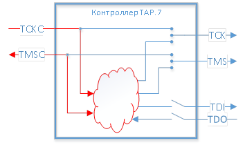
Instead of requiring chip designers to redo the entire JTAG logic, the standard suggests adding an adapter that converts the two-wire interface into a regular four-wire interface:
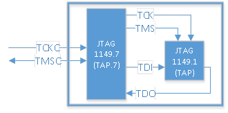
This adapter contains its own Test Access Port (TAP), called TAP.7, so that you can distinguish it from regular TAP (aka TAP.1). The TAP.7 controller inside is exactly the same machine as TAP.1, but there are some differences, for example, it does not have an Instruction Register, but there are many other registers that TAP.1 does not have.
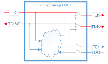
By default, TAP.7 is transparent, i.e. the TCKC signal is simply directly connected to the TCK, and the TMSC to the TMS. Therefore, all signals sent by TCKC and TMSC are transmitted without any changes to TCK and TMS:
Obviously, when trying to transmit an Oscan1 packet in this mode, “nTDI” will be perceived by the TAP.1 controller simply as the first bit transmitted over the TMS line, “TMS” as the second bit, etc. That is why, before transmitting packets, you need to transfer the TAP.7 controller to “advanced mode”. This is done by writing to one of the internal TAP registers. 7. During configuration, TCK and TMS are disabled (and TDI and TDO were disabled before):
After the configuration is completed, TCK, TMS, TDI and TDO are controlled by the internal logic of the controller:

Thus, the process of switching to "advanced mode" and the subsequent reading of IDCODE looks like this:
- Initialize the TAP.7 and TAP.1 controllers
- Disable TCK and TMS
- Select the desired transmission format
- If OScan, MScan or SScan format is selected, then switch to “advanced mode”
- Connect TCK, TMS, TDI and TDO
- Record the IDCODE address in the Instruction Register
- Read data from IDCODE
Initializing TAP. 7. Escape Reset
Since you can never know what state the TAP.7 and TAP.1 machines are in, you must reset them before starting work. To reset the TAP.7 controller, Escape Reset is used - one of the types of escape sequences defined by the standard. Escape sequences differ from all other JTAG commands in that TMS values are not read from the leading edge of TCK, but asynchronously. The TAP.7 controller counts the number of edges of the TMS signal that have arrived while the TCKC is unchanged. The number of fronts determines the type of escape sequence. For Escape Reset, it must be more than seven:
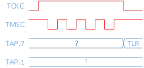
Escape Reset also puts TAP.7 in the Test Logic Reset state. The beauty of escape sequences is that they have absolutely no effect on TAP.1, which simply ignores them. TAP.1 reads TMS values only on the rising edge of TCK, so it doesn't care what happens to TMS the rest of the time.
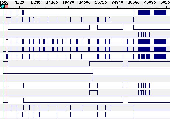
This is how the Escape Reset looks on the oscilloscope screen, which transfers the Digilent HS2 USB-JTAG adapter :

As you can see, all eight fronts are in place, but the distance between the sixth and seventh looks suspicious. I already complained to Digilent - they promised to fix it.
Initializing TAP.1
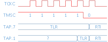
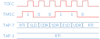
To reset TAP.1 after TAP.7, the standard recommends sending five units via TMSC: they are guaranteed to transfer the TAP controller to Test-Logic-Reset from absolutely any other state (you can check it yourself):

Since we are not planning to return to Test-Logic-Reset anymore, it makes sense to send a zero after five units and thereby put the machine into Run-Test / Idle state. Let me remind you that the controller reads the TMS values at the moment of the leading edge of the TCK and immediately changes the state of the machine in accordance with these values:
Disabling TCK and TMS
To disable TCM and TMS, you need to transfer the TAP.7 controller to Control Mode 2. In total, the controller supports eight different Control Modes, numbered from zero to seven. We are interested in Control Mode 2, since only in it access to the service registers of the controller appears, one of which we need to change the packet format on OScan1.
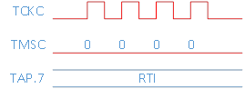
Switching between Control Modes is carried out sequentially by performing the so-called Zero-bit DR Shift (ZBS). Each ZBS performed increases the Control Mode by one. Unlike escape sequences, in theory, ZBS can affect the TAP.1 controller, but in practice this is highly unlikely. From the point of view of the IEEE 1149.1 standard, Zero-bit DR Shift makes absolutely no sense, so the developers hoped that neither the hardware nor the software developed before the 2-wire JTAG should use ZBS for any of their needs . On a timeline, ZBS looks like this:
As you can see, ZBS starts and ends in Run-Test / Idle state, so it is important not to forget after Escape Reset and Test-Logic-Reset to go to Run-Test / Idle before sending the first ZBS.
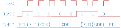
When the desired mode is selected, it must be locked (LOCK), after which subsequent ZBSs will no longer be able to influence the choice of mode. LOCK is almost the same as ZBS, only with the entry in Shift-DR:
Note that the state of TAP.1, unlike TAP.7, is no longer changing. This is because TCK and TMS are disabled immediately as soon as the Control Mode number becomes two, even if it is not already fixed.
Thus, to get into Control Mode 2, you need:
- Send two ZBS
- Send LOCK
Format selection
Now that we are in Control Mode 2, we can write to service registers. The standard describes many registers that are written to by special commands. Teams are divided into two groups - two-part (two-part command) and three-section (three-part command), which I will not consider.
For two-section teams, the number of the command is transmitted in the first section, and data in the second. Both sections are transmitted in the same way: from the Run-Test / Idle state, go to Shift-DR, and then return to Run-Test / Idle. The transmitted value is equal to the number of measures spent in Shift-DR.
We are interested in the command number three - STFMT (Store Scan Format), which writes the number of the desired format (for OScan1 it is nine), transmitted in the second section, to the SCNFMT (Scan Format) register.
Thus, in the first section we need to pass the three, and in the second - nine. First, write down the command number, for which we are waiting for three measures in the Shift-DR state (the TAP.1 state is not shown, since it does not change):
Then we write the data (nine measures in the Shift-DR state):

Writing to the SCNFMT register does not change the format per se. In order for the controller to switch the format, a special check packet must be sent.
Check packet
The verification package checks the settings are correct, and if everything is in order, the controller switches the format and, if necessary, switches to the “advanced mode”. Like everything else in IEEE 1149.7, the test suite has tons of different options. You will have to take my word for it that we need a package with an END directive (and do not ask what this means), which looks like this:
Hooray, now we are in “advanced mode” and can finally use OScan1! To return to "standard mode", just go to Test-Logic-Reset.
Connect TCK, TMS, TDI and TDO
So, we are in “advanced mode”, but still in Control Mode 2, which means that TAP.1 is still disabled, and we can’t read IDCODE from it. The standard describes four ways to exit Control Mode:
- Go to Test-Logic-Reset
- Go to Select-IR-Scan
- Write a unit to the ECL register (Exit Control Level) using the two-section STMC command
- To do something unknown related to the synchronization of TAP.7 controllers
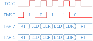
In Test-Logic-Reset we can’t, otherwise the controller will return to “standard mode”. Send a two-section command for a long time. But going to Select-IR-Scan and returning to Run-Test / Idle without going through Test-Logic-Reset is quite simple - you just need to send sequence 011011 via TMS (it’s not necessary to enter Shift-IR). Remember that in JTAG the low-order bit is always transmitted first:
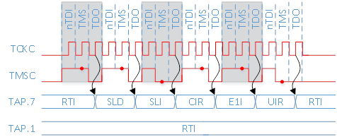
Red dots indicate the places where the controller reads the TMS bits from the TMSC input. Zeros are transmitted via TDI (i.e., in all packets, the nTDI bits are equal to one), although they are still ignored, since we do not enter the Shift-IR state.
By the way, unlike the “standard mode”, the state of TAP.7 does not change immediately after receiving a new TMS bit, but along the third (last) leading edge of the TCKC in the OScan1 packet (these moments are shown by black arrows in the figure) - this is done for so that the controller manages to insert the TDO bit into the OScan1 packet and send it to the host (in this particular case, the controller returns zeros over TDO).
Reading IDCODE
Now that TAP.1 is reconnected to TAP.7, we can finally read the contents of the IDCODE register.
The IDCODE register address is not described in the standard, therefore it is different in all controllers (in my case it is four-bit and equal to 0xC). To make life easier for users, the Instruction Register is initialized with an IDCODE address in the Test-Logic-Reset state. However, in the Capture-IR state, the contents of the Instruction Register are overwritten with the number 0x1 (regardless of the length of the Instruction Register, its least significant bit is set to one, and all the others are set to zero) so that an open circuit can be detected during testing. Since we entered Capture-IR at the previous stage, the IDCODE address is already overwritten, so you need to rewrite it first.
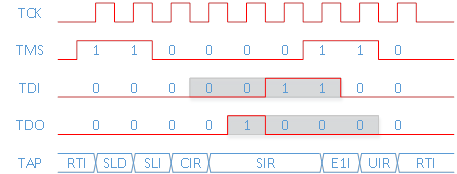
To write the register address, you need to enter the Shift-IR state and push the address (0xC) by TDI low bit forward. At the same time, the value that was in the Instruction Register before that, i.e. 0x1 (again, the least significant bit forward). In the case of a conventional four-wire JTAG IEEE 1149.1, it would look like this:
And this is how it looks when using OScan1 packages:
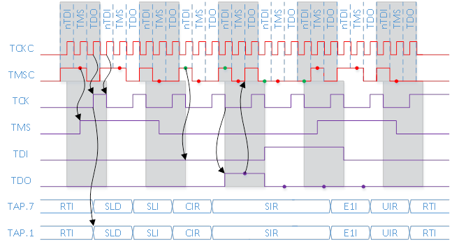
The red dots mark the places where the controller reads the TMS bits, and the green dots the nTDI bits from the TMSC input. The purple dots indicate the places where the controller reads the TDO bits before inserting them into OScan1 packets.
The arrows show some dependencies, for example, the TMS and TDI signals change along the corresponding edges of the TCKC, and the TDO signal changes along the trailing edge of the TCK.
Now it remains only to go into the Shift-DR state, push 32 arbitrary bits over TDI and read 32 bits from TDO, which will contain IDCODE. With your permission I will not give a temporary reading diagram for IDCODE.
Conclusion
I described about 5% of the capabilities of IEEE 1149.7. Nevertheless, I hope that you have some understanding of the principles underlying it.
All the diagrams in this article were tested on real hardware using the Digilent HS2 USB-JTAG adapter, the commercial 2-wire JTAG controller, which I have access to the source code, an FPGA debug board and Xilinx ChipScope logic analyzer.
The program for generating sequences was written using the API for HS2 based on an example that can be downloaded with the Digilent Adept SDK and worked fine both under Linux and under Windows.