We disassemble Sony Xperia Z2, the new flagship with an unusual cooling system
I came across a Sony Xperia Z2 smartphone that was not yet on sale in Russia. This is an updated and improved version of the six-month-old Xperia Z1, and if between Z and Z1 the difference was quite significant, then between Z1 and Z2 it may not be noticed at first glance. However, if you are not too lazy to look inside, confusing the updated flagship with its predecessor is impossible with all desire. If only because before in the smartphones of Sony, and other major brands, thermal copper tubes have never been found ...

The differences between Z2 and Z1 configuration can be listed in one paragraph. The diagonal of the Z2 screen is 5.2 inches instead of 5, but the resolution remains the same, 1920 x 1080 pixels. Instead of TFT, an IPS matrix with large viewing angles is used. The 20.7-megapixel camera can now record video in 4k (Ultra HD) format, but the module itself remains the same. The Qualcomm Snapdragon 800 chipset changed to the Snapdragon 801, and the amount of RAM increased from 2 to 3 GB. The battery capacity also increased slightly: from 3,000 to 3,200 mAh.
Is the above enough to call the Z2 a novelty? I do not know yet, it is necessary to check in work. In the meantime, let's see together what the next Sony flagship has inside. I note that I also disassembled Z1, and you can read / see the result here .
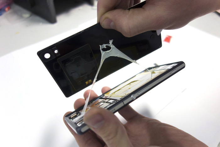
Dismantling the Z2 is a bit more complicated than its predecessor. As in the previous version, water resistance is provided by double-sided tape around the perimeter of the back cover, but now the latter is glued to the battery. From the point of view of reliability and structural rigidity, it is an exclusively correct decision.
Let's pay attention to the changed shape and the increased NFC antenna. Now, when pairing with different equipment, finding the right point for contact will be a little easier.

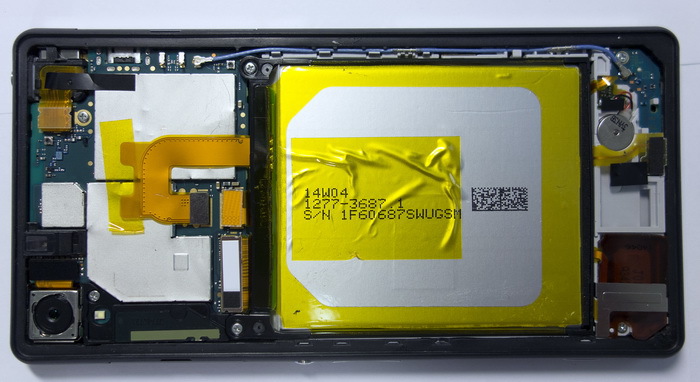
The battery has slightly increased in size. But not very significant, in accordance with the increase in capacity.

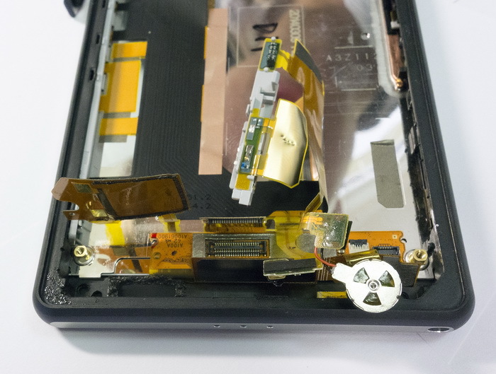
We remove it and ... wow! Copper heat pipe! Exactly the same as in the radiators of powerful coolers in a computer or on the motherboard. Just a little smaller.
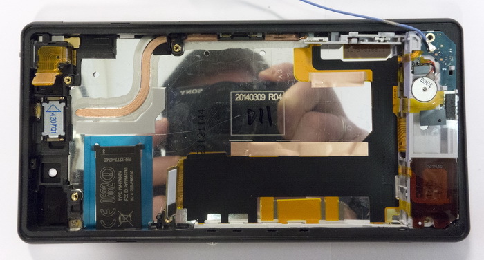
The handset is long and soldered on the back of the screen. So it is he who performs the role of a radiator. An unusual solution, frankly. I’ll definitely check how this affects the temperature of the screen itself, does it burn my cheek if someone calls at the height of a game session in Asphalt 8. Most likely, this will not happen, because the area of heat dissipation is quite large. And yet - an amazing solution. Just amazing. Involuntarily, the question arises - will not powerful portable dropsy be needed for powerful eight-core processors with ARM architecture? (By the way, we already had such an experience - remember last year's NEC Medias X N-06E smartphone).
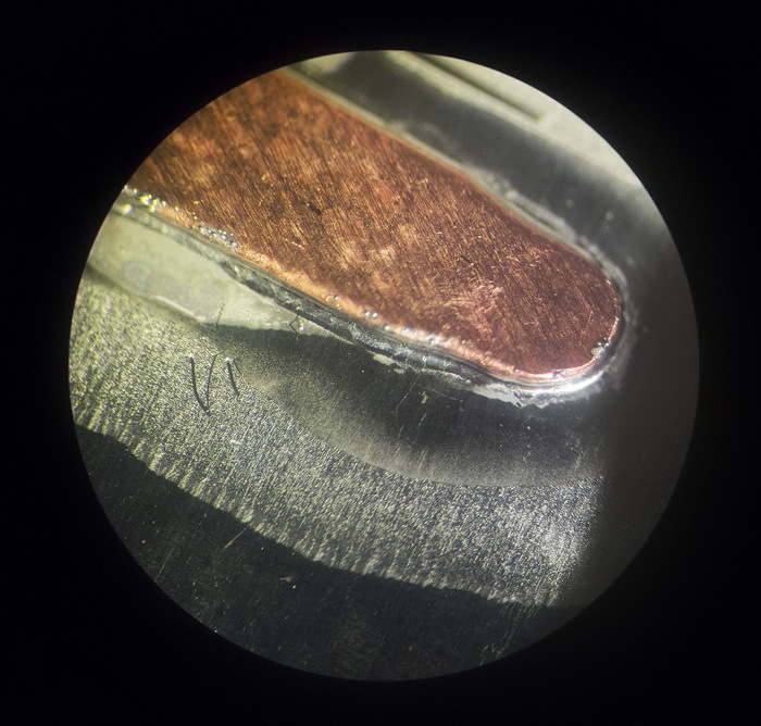
In a microscope, you can see how the tube is soldered to the surface.
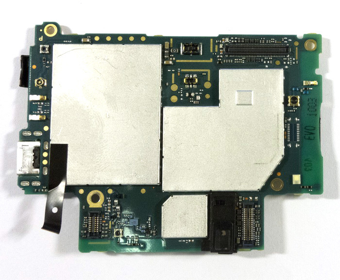
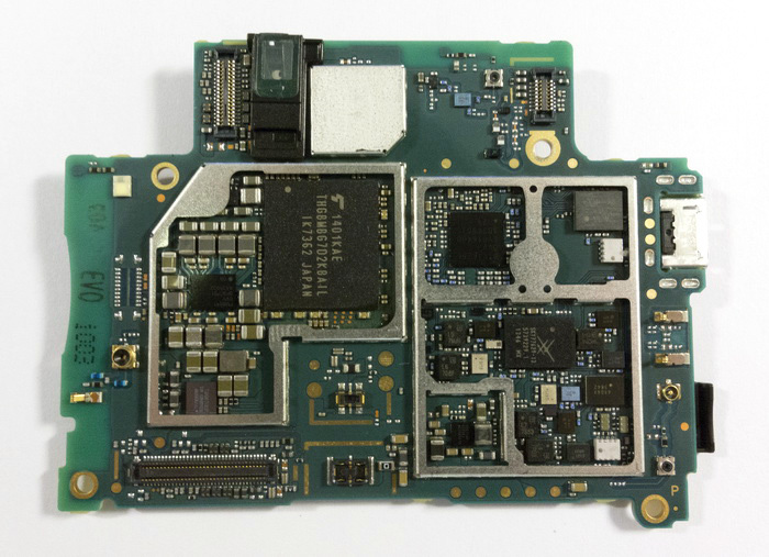
The motherboard in form and layout is significantly different from its predecessor in Z1. Components are more compact, and protruding thin pieces of PCB have also disappeared. But the thermal paste between the chips and the heat-scattering screens remained, now there is no way without it.
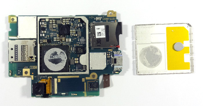
Under the microscope, you can see the Qualcomm MSM8974AB chip hiding under the RAM module. Such "modesty" is the standard, and therefore it is impossible to see the entire chip without ruining the board. In some Huawei products, the SoC and the memory module are placed nearby, however, this is due to the fact that the SoC manufacturing process is quite ancient and a “sandwich” cannot be made normally.

If the motherboard has become more durable, then the loops on the contrary made it thinner. They look rather flimsy, and when disassembling / assembling it took a fair amount of accuracy so as not to damage anything. Probably, if you do not get into the smartphone with inept hands, they will last as long as necessary, and yet ... it’s flimsy.
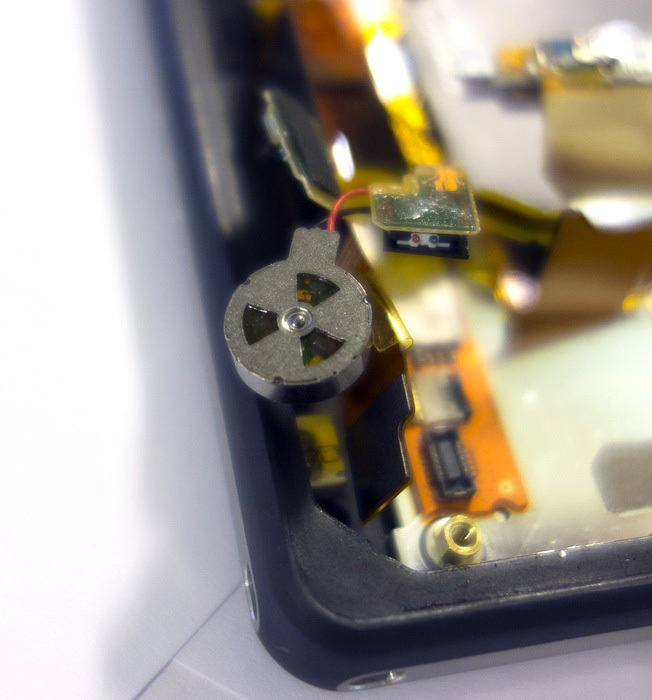
We drew attention to the unusual design of the vibration motor. From the back of it, there are three cutouts, which make you remember either the game about Duke Nukem, or just a sign of radiation hazard.
When viewed under a microscope, nothing unusual in the design could be noticed.

There may be several options: either Sony decided to amplify the sound from the motor in vibration mode, or it is corny to save metal.
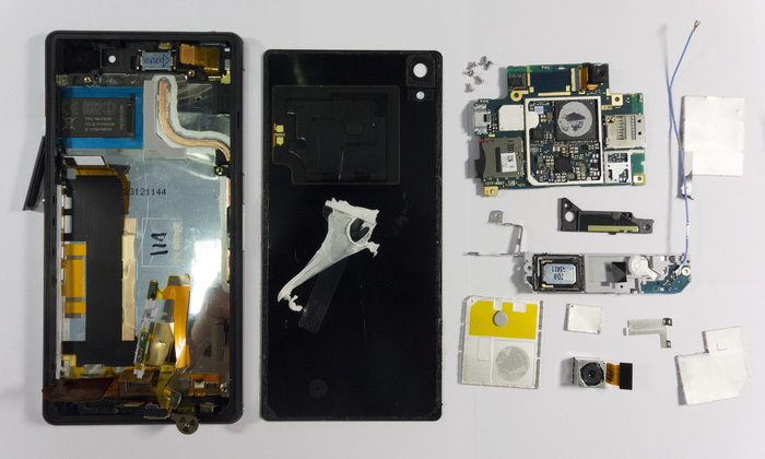
Xperia Z2 - the fourth Sony device, which I disassemble over the past six months. One cannot fail to note the progress in the engineering culture of the developers: if the Xperia Z Ultra from the inside looked quite ... eclectic , then in the Z1 and especially the Z1 Compact there was an increasingly systematic approach to placing components on the board and inside the case. Z2, frankly, is still far from the beauty of the internal design to Apple products. But the pursuit of beauty is evident.
From the point of view of maintainability, the device is on the same level as Z1. It’s a little easier to change the screen, because now the latter rests on latches and is removed relatively easily. But this is “compensated” by a more complicated system of fragile loops. So it’s better not to go inside yourself. Even if there is a professional soldering station at home.
About user impressions of the smartphone (yes, it is assembled back and works fine) I will write in ten days. I don’t feel like rushing, especially since the device will go on sale only in May.
Update: You can read about my user experiences here .
The author thanks for the help in preparing the material by Alexander Levchenko (www.tech-town.ru )
The differences between Z2 and Z1 configuration can be listed in one paragraph. The diagonal of the Z2 screen is 5.2 inches instead of 5, but the resolution remains the same, 1920 x 1080 pixels. Instead of TFT, an IPS matrix with large viewing angles is used. The 20.7-megapixel camera can now record video in 4k (Ultra HD) format, but the module itself remains the same. The Qualcomm Snapdragon 800 chipset changed to the Snapdragon 801, and the amount of RAM increased from 2 to 3 GB. The battery capacity also increased slightly: from 3,000 to 3,200 mAh.
Is the above enough to call the Z2 a novelty? I do not know yet, it is necessary to check in work. In the meantime, let's see together what the next Sony flagship has inside. I note that I also disassembled Z1, and you can read / see the result here .
Dismantling the Z2 is a bit more complicated than its predecessor. As in the previous version, water resistance is provided by double-sided tape around the perimeter of the back cover, but now the latter is glued to the battery. From the point of view of reliability and structural rigidity, it is an exclusively correct decision.
Let's pay attention to the changed shape and the increased NFC antenna. Now, when pairing with different equipment, finding the right point for contact will be a little easier.
The battery has slightly increased in size. But not very significant, in accordance with the increase in capacity.
We remove it and ... wow! Copper heat pipe! Exactly the same as in the radiators of powerful coolers in a computer or on the motherboard. Just a little smaller.
The handset is long and soldered on the back of the screen. So it is he who performs the role of a radiator. An unusual solution, frankly. I’ll definitely check how this affects the temperature of the screen itself, does it burn my cheek if someone calls at the height of a game session in Asphalt 8. Most likely, this will not happen, because the area of heat dissipation is quite large. And yet - an amazing solution. Just amazing. Involuntarily, the question arises - will not powerful portable dropsy be needed for powerful eight-core processors with ARM architecture? (By the way, we already had such an experience - remember last year's NEC Medias X N-06E smartphone).
In a microscope, you can see how the tube is soldered to the surface.
The motherboard in form and layout is significantly different from its predecessor in Z1. Components are more compact, and protruding thin pieces of PCB have also disappeared. But the thermal paste between the chips and the heat-scattering screens remained, now there is no way without it.
Under the microscope, you can see the Qualcomm MSM8974AB chip hiding under the RAM module. Such "modesty" is the standard, and therefore it is impossible to see the entire chip without ruining the board. In some Huawei products, the SoC and the memory module are placed nearby, however, this is due to the fact that the SoC manufacturing process is quite ancient and a “sandwich” cannot be made normally.
If the motherboard has become more durable, then the loops on the contrary made it thinner. They look rather flimsy, and when disassembling / assembling it took a fair amount of accuracy so as not to damage anything. Probably, if you do not get into the smartphone with inept hands, they will last as long as necessary, and yet ... it’s flimsy.
We drew attention to the unusual design of the vibration motor. From the back of it, there are three cutouts, which make you remember either the game about Duke Nukem, or just a sign of radiation hazard.
When viewed under a microscope, nothing unusual in the design could be noticed.
There may be several options: either Sony decided to amplify the sound from the motor in vibration mode, or it is corny to save metal.
Xperia Z2 - the fourth Sony device, which I disassemble over the past six months. One cannot fail to note the progress in the engineering culture of the developers: if the Xperia Z Ultra from the inside looked quite ... eclectic , then in the Z1 and especially the Z1 Compact there was an increasingly systematic approach to placing components on the board and inside the case. Z2, frankly, is still far from the beauty of the internal design to Apple products. But the pursuit of beauty is evident.
From the point of view of maintainability, the device is on the same level as Z1. It’s a little easier to change the screen, because now the latter rests on latches and is removed relatively easily. But this is “compensated” by a more complicated system of fragile loops. So it’s better not to go inside yourself. Even if there is a professional soldering station at home.
About user impressions of the smartphone (yes, it is assembled back and works fine) I will write in ten days. I don’t feel like rushing, especially since the device will go on sale only in May.
Update: You can read about my user experiences here .
The author thanks for the help in preparing the material by Alexander Levchenko (www.tech-town.ru )