Major changes in leading chip architectures
- Transfer
The introduction of AI at the chip level allows you to process locally more data, because the increase in the number of devices no longer gives the same effect
Chip makers are working on new architectures that significantly increase the amount of data processed per watt and clock. The ground is being prepared for one of the largest revolutions in chip architecture in recent decades.
All major manufacturers of chips and systems change the direction of development. They entered the architecture race, which involves changing the paradigm in everything: from reading and writing to memory, processing them and, ultimately, assembling the various elements on the chip. Although the miniaturization continues, no one relies on scaling to cope with the explosive growth of data from sensors and the increase in traffic between machines.
Among the changes in new architectures:
- New methods for processing more data per cycle, sometimes with less accuracy or by prioritizing certain operations, depending on the application.
- New memory architectures that change the way data is stored, read, written and accessed.
- More specialized processing modules, located throughout the system close to the memory. Instead of a central processor, accelerators are selected depending on the type of data and the application.
- In the field of AI, work is underway to combine different types of data in the form of templates, which effectively increases the data density while minimizing the differences between different types.
- Now the package layout is the main component of the architecture, with more and more attention being paid to the simplicity of changing these structures.
“There are several trends that influence technical progress,” said Steven Wu, an outstanding engineer at Rambus. - In data centers, you squeeze the maximum out of hardware and software. From this angle, data center owners look at the economy. Implementing something new is expensive. But bottlenecks are changing, so specialized chips are being introduced for more efficient calculations. And if you reduce data flows back and forth to I / O and memory, this can have a big impact. ”
Changes are more obvious at the edge of the computing infrastructure, that is, among the terminal sensors. Manufacturers have suddenly realized that tens of billions of devices will generate too much data: this amount cannot be sent to the cloud for processing. But processing all this data on the edge introduces other problems: it requires major improvements in performance without a strong increase in power consumption.
“There is a noticeable trend towards lower accuracy,” said Robert Ober, lead architect of the Tesla platform at Nvidia. - This is not just computational cycles. This is more intensive packing of data in memory, where the format of 16-bit commands is used. ”
Ober believes that due to a series of architectural optimizations, it is possible in the foreseeable future to double the processing speed every couple of years. “We will see a dramatic increase in productivity,” he said. - For this you need to do three things. The first is computing. The second is memory. The third area is host and I / O bandwidth. Much work needs to be done to optimize storage and the network stack. ”
Something is already being implemented. In a presentation at the Hot Chips 2018 conference, Jeff Ruppley, the lead architect for Samsung's research center in Austin, pointed out several major architectural changes in the M3 processor. One includes more instructions per clock — six instead of four in the past M2 chip. In addition, branch prediction on neural networks was implemented and the queue of instructions was doubled.
Such changes shift the point of innovation from direct manufacturing of microchips to architecture and design on the one hand and to the layout of elements on the other side of the production chain. And although in technological processes innovations will also continue, but it is incredibly difficult to achieve increased productivity and power by 15–20% in each new chip model - and this is not enough to cope with the rapid growth of data.
“Changes are occurring at an exponential rate,” said Victor Pen, president and CEO of Xilinx, in a speech at the Hot Chips conference. “Each year, 10 zettabytes [10 21 bytes] of data will be generated , and most of it in an unstructured form.”
New approaches to memory
Dealing with so much data requires rethinking every component in the system, from data processing methods to storage.
“There have been many attempts to create new memory architectures,” said Carlos Machin, senior director of innovation, eSilicon EMEA. - The problem is that you need to read all the lines and select one bit in each. One option is to create a memory that can be read from left to right, as well as up and down. You can go even further and add computation to memory. ”
These changes include changing the memory reading methods, the location and type of processing elements, and the introduction of AI to determine the priorities for storing, processing, and moving data throughout the system.
"What if in the case of sparse data we can read from this array only one byte at a time - or maybe eight consecutive bytes from the same byte path, without wasting energy on other bytes or byte paths that we are not interested in ? - asks Mark Greenberg, director of product marketing for Cadence. - In the future this is possible. If you look at the HBM2 architecture, for example, then the stack is organized in 16 virtual channels of 64 bits each, and you only need to get 4 consecutive 64-bit words to access any virtual channel. Thus, it is possible to create data arrays with a width of 1024 bits, write horizontally, but read vertically four 64-bit words at a time. "
Memory is one of the main components of the von Neumann architecture, but now it has also become one of the main areas for experimentation. "The main enemy is virtual memory systems, where data is moved in more unnatural ways," said Dan Bouvier, chief architect of AMD client products. - This is a broadcast broadcast. We are used to this in the field of graphics. But if we eliminate conflicts in the DRAM memory bank, we will get much more efficient streaming. Then a separate GPU can use DRAM in the range of 90% efficiency, which is very good. But if you streamline streaming seamlessly, the CPU and APU will also fall in the efficiency range from 80% to 85%. ”
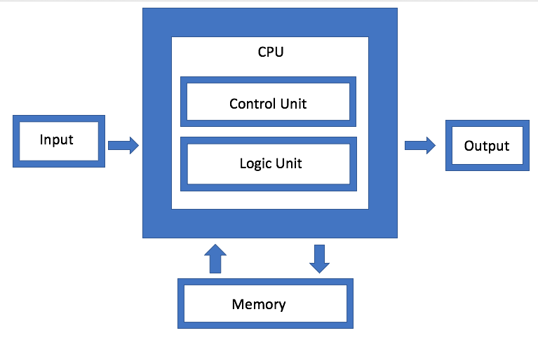
Fig. 1. Architecture von Neumann. Source: Semiconductor Engineering
IBM is developing a different type of memory architecture, which is essentially an upgraded version of disk pooling. The goal is that instead of using a single disk, the system can arbitrarily use any available memory through a connector, which Jeff Stucheli, architect of IBM's hardware systems, calls the “Swiss Army Knife” for the connectivity of the elements. The advantage of the approach is that it allows you to mix and combine different types of data.
“The processor is becoming the center of a high-performance signaling interface,” says Stucheli. “If you change the micro-architecture, then the core performs more operations per cycle on the same frequency.”
Connectivity and bandwidth should ensure the processing of a dramatically increased amount of generated data. “The main bottlenecks are now in the data movement sites,” said Wu from Rambus. - The industry has done a great job increasing the speed of the calculations. But if you are expecting data or specialized data patterns, then you need to run memory faster. Thus, if you look at DRAM and NVM, performance depends on the traffic pattern. If the data is streaming, the memory will provide very good performance. But if the data comes in random drops, it is less effective. And whatever you do, with an increase in volume, you still have to do it faster. ”
More calculations, less traffic
The problem is exacerbated by the fact that there are several different types of data generated at different frequencies and speeds by devices on the edge. In order for this data to flow freely between different processing modules, management must become much more efficient than in the past.
“There are four basic configurations: many-to-many (many-to-many), memory subsystems, low-power IO, as well as grids and ring topologies,” says Charlie Janak, chairman and CEO of Arteris IP. - You can place all four on one chip, which is what happens with key IoT chips. Or you can add high bandwidth HBM subsystems. But the complexity is enormous, because some of these workloads are very specific, and the chip has several different work tasks. If you look at some of these microcircuits, they get huge amounts of data. This is in systems such as car radar and lidar. They cannot exist without some advanced interconnections. ”
The challenge is how to minimize the movement of data, but at the same time maximize the flow of data when it is needed - and somehow find a balance between local and centralized processing without excessive growth of energy consumption.
“On the one hand, this is a bandwidth problem,” said Rajesh Ramanujam, product marketing manager at NetSpeed Systems. “You want to reduce traffic whenever possible, so transfer data closer to the processor.” But if you still need to move the data, it is desirable to maximally condense them. But nothing exists by itself. Everything must be planned from the system level. At each step, several interdependent axes must be considered. They determine whether you are using the memory in the traditional way of reading-writing or you are using new technologies. In some cases, it may be necessary to change the way the data itself is stored. If you need higher performance, it usually means an increase in the area of the chip, which affects heat dissipation. And now, taking into account functional safety, data overload cannot be allowed. ”
That is why so much attention is paid to data processing at the edge and throughput of channels by various data processing modules. But as far as the development of different architectures is very different, how and where this data processing is implemented.
For example, Marvell introduced an SSD controller with integrated AI to cope with the large computational load on the edge. The AI engine can be used for analytics right inside the SSD drive.
“You can load models directly into the hardware and perform hardware processing on the SSD controller,” said Nedarnica, Marvell’s chief engineer. - Today it makes the server in the cloud (host). But if each disk will send data to the cloud, it will create a huge amount of network traffic. It is better to perform processing on the edge, and the host issues only the command, which is simply metadata. The more drives you have, the more processing power. This is a huge benefit from reducing traffic. ”
In this approach, it is especially interesting that it adapts to different data depending on the application. So, a host can generate a task and send it to a storage device for processing, after which only metadata or calculation results are sent back. In another scenario, the storage device can store data, pre-process it, and generate metadata, tags, and indexes, which are then retrieved by the host as needed for further analytics.
This is one of the possible options. There are others. Samsung Rupley stressed the importance of processing and merging idioms, which can decode two instructions and combine them into one operation.
AI is in control and optimization.
Artificial Intelligence is applied at all optimization levels - this is one of the truly new elements in the chip architecture. Instead of allowing the operating system and middleware to control functions, this monitoring function is distributed across the chip, between chips, and at the system level. In some cases, hardware neural networks are being introduced.
“It's not so much about packing more elements together as changing traditional architecture,” says Mike Gianfanya, vice president of marketing for eSilicon. - With the help of AI and machine learning, you can distribute elements across the system, getting more efficient processing with prediction. Or you can use separate chips that function independently in the system or in a module. ”
ARM has developed its first machine learning chip, which it plans to launch at the end of this year for several markets. “This is a new type of processor,” said Ian Bratt, honored ARM engineer. - It includes a fundamental unit - this is a computational engine, as well as a MAC engine, a DMA engine with a control module and a broadcast network. In total there are 16 cores made using the 7 nm process technology, which provide 4 TeraOps at 1 GHz. ”
Since ARM works with a partner ecosystem, its chip is more versatile and customizable than other AI / ML chips that are being developed. Instead of a monolithic structure, it divides processing into functions, so each computational module operates on a separate feature map. Bratt named four key ingredients: static planning, effective coagulation, band narrowing mechanisms, and programmed adaptation to future design changes.
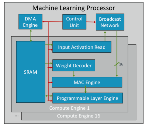
Fig. 2. ML processor architecture from ARM. Source: ARM / Hot Chips
Meanwhile, Nvidia chose a different tactic: creating a dedicated deep learning engine next to the GPU to optimize image and video processing.
Conclusion
Using some or all of these approaches, chip manufacturers expect to double their performance every couple of years, keeping up with the explosive growth of data, while remaining in the tight framework of energy consumption budgets. But this is not just more computation. This is a change in the design platform of chips and systems, when the main factor is the growing amount of data, and not the limitations of hardware and software.
“When computers appeared in companies, it seemed to many that the world around us accelerated,” said Aart de Gees, chairman and one of the executive directors of Synopsys. - They made accounting on pieces of paper with piles of books. Ledger turned into a stack of punch cards for printing and calculation. There has been a tremendous change, and we see it again. With the advent of simple computing computers, the algorithm of actions has not changed mentally: you could follow every step. But now something else is happening that could lead to a new acceleration. It's like on an agricultural field to turn on watering and apply a certain type of fertilizer only on a certain day, when the temperature reaches the desired level. This use of machine learning is an optimization that was not obvious in the past. ”
He is not alone in this assessment. “New architectures will be adopted,” said Wally Rines, President and CEO of Mentor, Siemens Business. - They will be designed. Machine learning will be used in many or most cases because your brain learns from experience. I visited 20 or more companies that develop specialized AI processors of one sort or another, and each one has its own little niche. But you will increasingly see their use in specific applications, and they will complement the traditional von Neumann architecture. Neuromorphic calculations will become mainstream. This is a big step in computing efficiency and cost reduction. Mobile devices and sensors will start doing the work that servers are doing today. ”