Resolving naming conventions in Quartus II using Schematic
Hello, Habrosociety.
I would like to share with you a solution to one problem that I have encountered and which I have been solving for quite some time. And a lot of different radio electronics specialists (to whom I turned for help and advice), as well as 2 domestic and 1 foreign forums on radio electronics could not help solve this problem.
I want to make sure that whoever reads this never "gets on the rake" that I got up on and suffered with for a long time.
The problem was that I could not use more than 1 pin on one IDC connector. If more than 1 pin (2 or more) was used on the connector, then the connector was silent during the test with an oscilloscope.
As it turned out now, the problem was the naming rules in Quartus II when using Schematic.
To all those to whom it will be useful or interesting - I ask for a cat.
I also encountered this problem on target (handmade) devices. But for clarity, I would like to demonstrate Altera DE1 on a whale (Figure 1).

Fig. 1 - Altera DE1 Development and Education Board
Uploaded to Quartus II the file "Altera_DE1_pin_assignments.csv" with assignment of FPGA pin (Name in the project - FPGA pin number), which he took from the disk from the whale.
In Figure 2, you can see the pin names of the forty-pin IDC connector “GPIO_0” in Pin Planner.
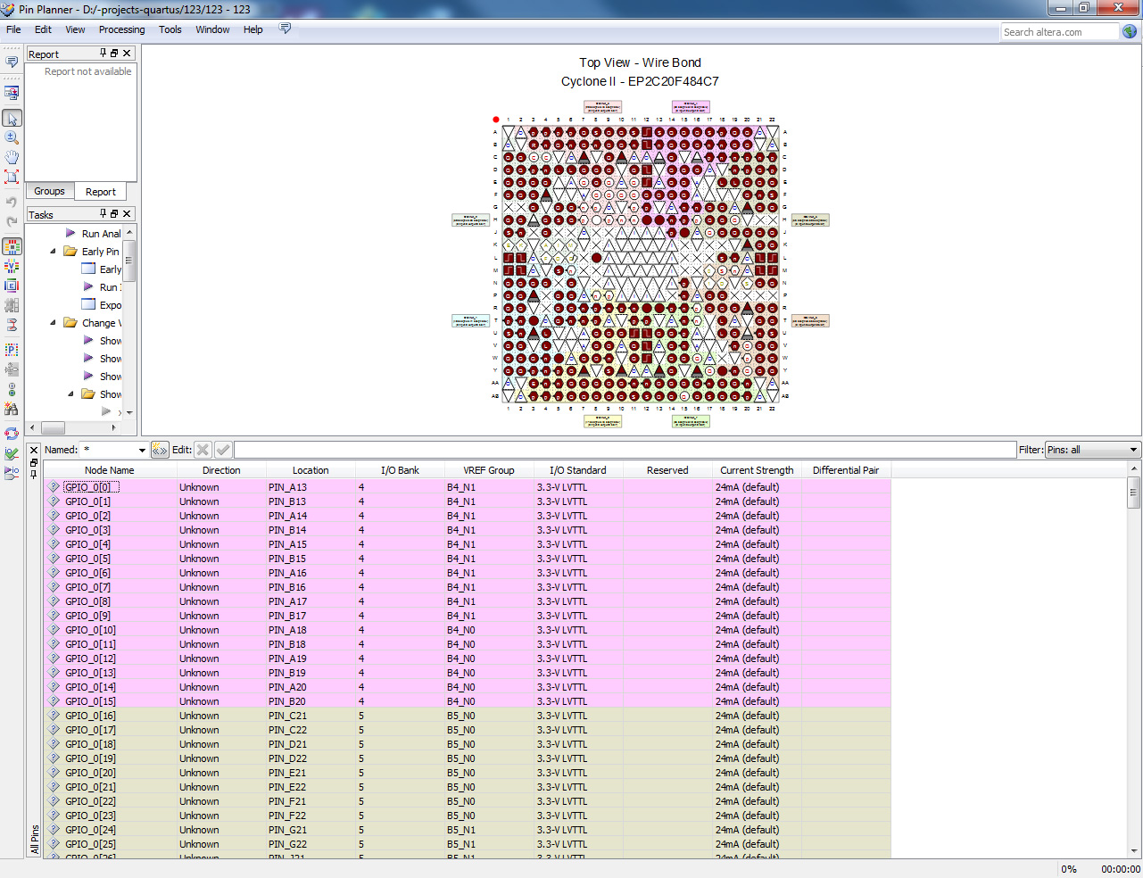
Fig. 2 - Quartus II Pin Planner for Altera DE1
For clarity, I will describe the problem in more detail on the project shown in Figure 3. From the “CLOCK_50” pin, a 50 MHz block comes (from the clock generator on the whale, which is connected to a specific FPGA pin). “Clock_50_to_1” is a handwritten module in Verilog language that converts a 50 MHz clock to 1 MHz clock via a counter (similar problems were observed when using the ALTPLL megafunction built into Quartus II). The converted clock is output to 2 IDC connectors - GPIO_0 and GPIO_1. On the GPIO_0 connector 1 pin is used ([1]) and everything works, on the GPIO_1 connector 2 pins are used ([1], [3]) and there is no signal.
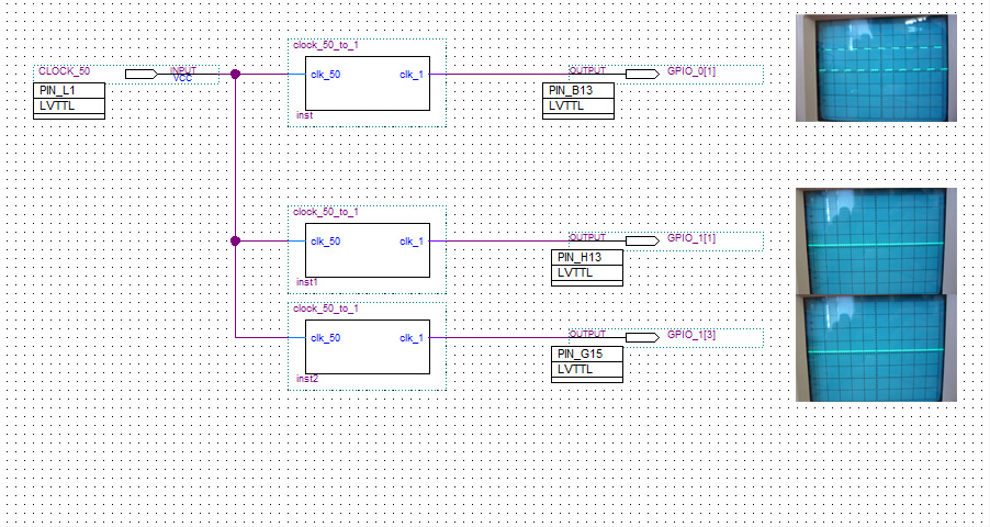
Fig. 3 - Screenshot of Quartus II and photos from the oscilloscope
One of the users of the Altera Forum , noticed “out of the corner” some strange warnings when compiling the project (which is shown in Figure 3) in Quartus II, and said: “I have not encountered this, I don’t know what to do, but I advise you to do the top-level module of the project is not in schematic, but in Verilog or VHDL. ”
In a word, after analyzing the warnings, it became clear that Quartus II renames
“GPIO_1 [1]” in “GPIO_11”,
“GPIO_1 [3]” to “GPIO_13”,
and there are no specific FPGA pins for GPIO_11 and GPIO_13.
So we found out that there are two renaming schemes - Max + Plus II and Quartus II.
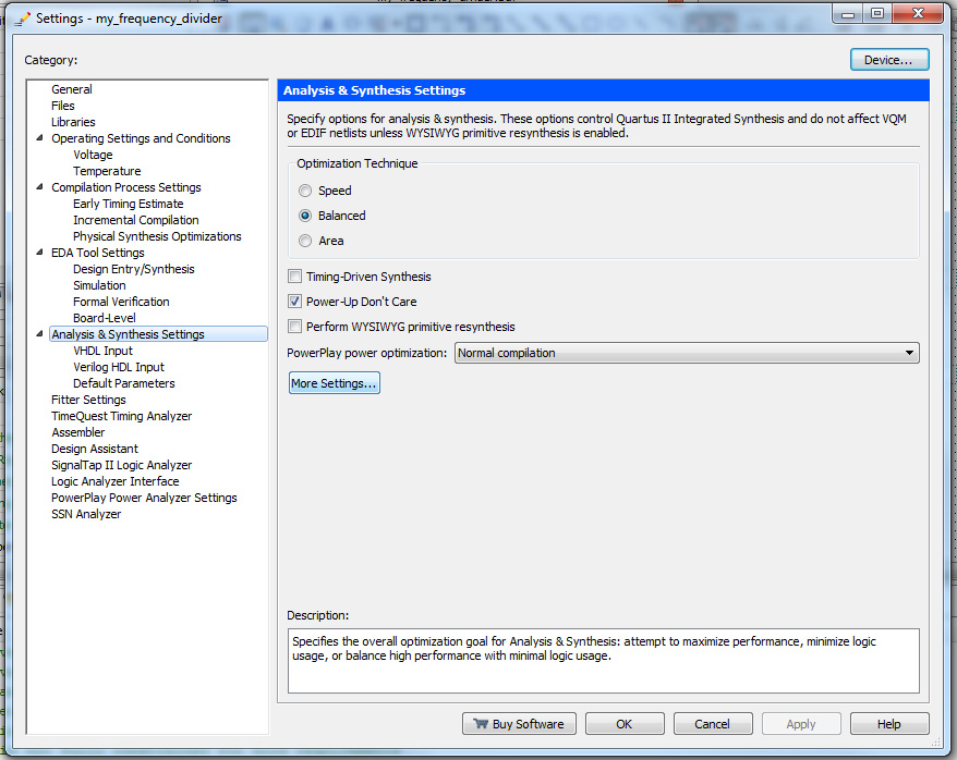
For a project, you can explicitly switch these naming schemes:
Assignments => Settings => Analysis & Synthesis Settings => More Settings => Block Design Naming
As can be seen from Figure 4, if you explicitly switch the renaming scheme to Quartus II, then the problem is solved.
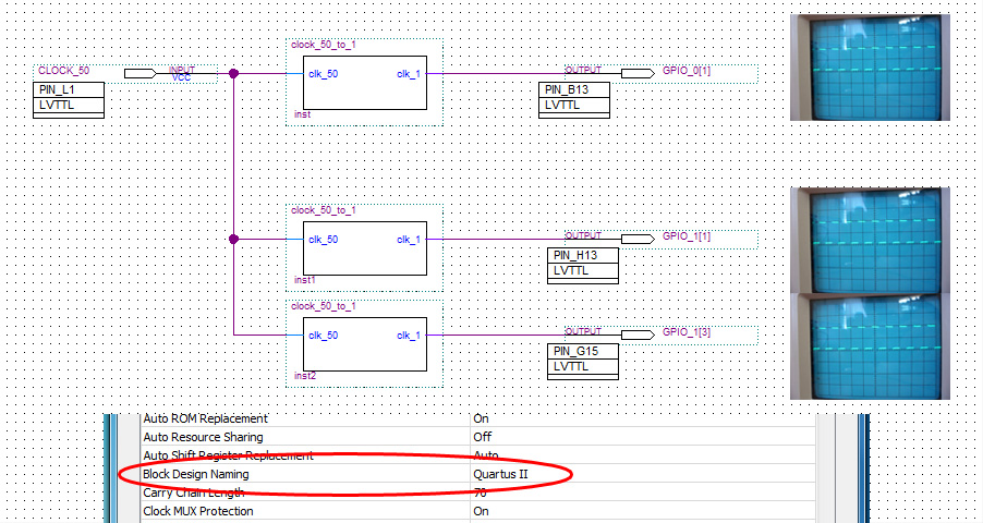
Fig. 4 - Screenshot of Quartus II and photos from the oscilloscope
If you start using the pins of the IDC connector in order (from 0 to n), then even with the Auto renaming scheme set, Quartus II will not rename anything.

Fig. 5 - Screenshot of Quartus II and photos from the oscilloscope
PS I will be very happy if I can make life easier for someone and save his time.
I would like to share with you a solution to one problem that I have encountered and which I have been solving for quite some time. And a lot of different radio electronics specialists (to whom I turned for help and advice), as well as 2 domestic and 1 foreign forums on radio electronics could not help solve this problem.
I want to make sure that whoever reads this never "gets on the rake" that I got up on and suffered with for a long time.
The problem was that I could not use more than 1 pin on one IDC connector. If more than 1 pin (2 or more) was used on the connector, then the connector was silent during the test with an oscilloscope.
As it turned out now, the problem was the naming rules in Quartus II when using Schematic.
To all those to whom it will be useful or interesting - I ask for a cat.
Problem demonstration
I also encountered this problem on target (handmade) devices. But for clarity, I would like to demonstrate Altera DE1 on a whale (Figure 1).
Fig. 1 - Altera DE1 Development and Education Board
Uploaded to Quartus II the file "Altera_DE1_pin_assignments.csv" with assignment of FPGA pin (Name in the project - FPGA pin number), which he took from the disk from the whale.
In Figure 2, you can see the pin names of the forty-pin IDC connector “GPIO_0” in Pin Planner.
Fig. 2 - Quartus II Pin Planner for Altera DE1
For clarity, I will describe the problem in more detail on the project shown in Figure 3. From the “CLOCK_50” pin, a 50 MHz block comes (from the clock generator on the whale, which is connected to a specific FPGA pin). “Clock_50_to_1” is a handwritten module in Verilog language that converts a 50 MHz clock to 1 MHz clock via a counter (similar problems were observed when using the ALTPLL megafunction built into Quartus II). The converted clock is output to 2 IDC connectors - GPIO_0 and GPIO_1. On the GPIO_0 connector 1 pin is used ([1]) and everything works, on the GPIO_1 connector 2 pins are used ([1], [3]) and there is no signal.
Fig. 3 - Screenshot of Quartus II and photos from the oscilloscope
For clarity, the picture in the spoiler shows a photograph of the connectors: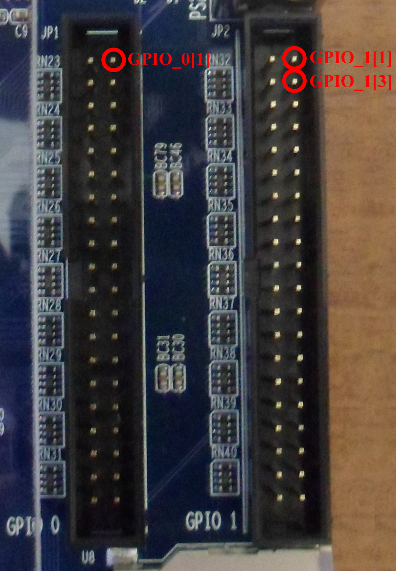
Cause of the problem
One of the users of the Altera Forum , noticed “out of the corner” some strange warnings when compiling the project (which is shown in Figure 3) in Quartus II, and said: “I have not encountered this, I don’t know what to do, but I advise you to do the top-level module of the project is not in schematic, but in Verilog or VHDL. ”
The warning text is as follows:
Warning (275080): Converted elements in bus name "GPIO_1" using legacy naming rules. Make any assignments on the new names, not on the original names.
Warning (275080): Converted elements in the bus named “GPIO_1” use inherited naming rules. Make any assignments for the new names, not the original names.
- Warning (275081): Converted element name (s) from “GPIO_1 [1]” to “GPIO_11”
- Warning (275081): Converting the element name from “GPIO_1 [1]” to “GPIO_11”
- Warning (275081): Converted element name (s) from “GPIO_1 [3]” to “GPIO_13”
- Warning (275081): Converting the element name from “GPIO_1 [3]” to “GPIO_13”
Critical Warning (169085): No exact pin location assignment (s) for 2 pins of 4 total pins
Warning of special importance (169085): The exact pin location (s) for 2 pins out of 4 pins in general
is not assigned - Info (169086): Pin GPIO_11 not assigned to an exact location on the device
- Information (169086): The exact location is not assigned pin GPIO_11 on the device
- Info (169086): Pin GPIO_13 not assigned to an exact location on the device - Information (169086): The exact location of pin GPIO_13 on the device
is not assigned
In a word, after analyzing the warnings, it became clear that Quartus II renames
“GPIO_1 [1]” in “GPIO_11”,
“GPIO_1 [3]” to “GPIO_13”,
and there are no specific FPGA pins for GPIO_11 and GPIO_13.
What the Altera Knowledge Base says about this:
The Max + Plus II software has limited support for bus names in the schematic and will sometimes rename elements in the bus to work within these limits.
For example, Max + Plus II software would rename the bus names a [1..0], b [1], b [0] to a1, a0, b1, b0, respectively.
Quartus II software initially retained this behavior for backward compatibility, but now supports a method that stores the natural bus names (with square brackets) in your project.
However, to avoid changing software behavior for existing projects, Quartus II continues to use the older naming conventions for inheriting BDF (Block Design File) and GDF (Graphic Design File) project files.
For the new schematic, Quartus II software saves the real names (with square brackets) in the project at compile time.
Naming rules for Quartus II version 7.1 and earlier:
(RENAME DIAGRAM Max + Plus II):
If the bus a [0..3] is broken into parts, then 4 pins are created: a0, a1, a2, a3
Naming rules for Quartus II version 7.2 and later:
(Quartus II RENAME DIAGRAM):
If the bus a [0..3] is split into parts, then 4 pins are created: a [0], a [1], a [2], a [ 3]
The way to solve the problem №1
So we found out that there are two renaming schemes - Max + Plus II and Quartus II.
For a project, you can explicitly switch these naming schemes:
Assignments => Settings => Analysis & Synthesis Settings => More Settings => Block Design Naming
For clarity, in the spoiler, screenshots of switching the renaming rules in steps: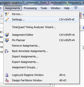
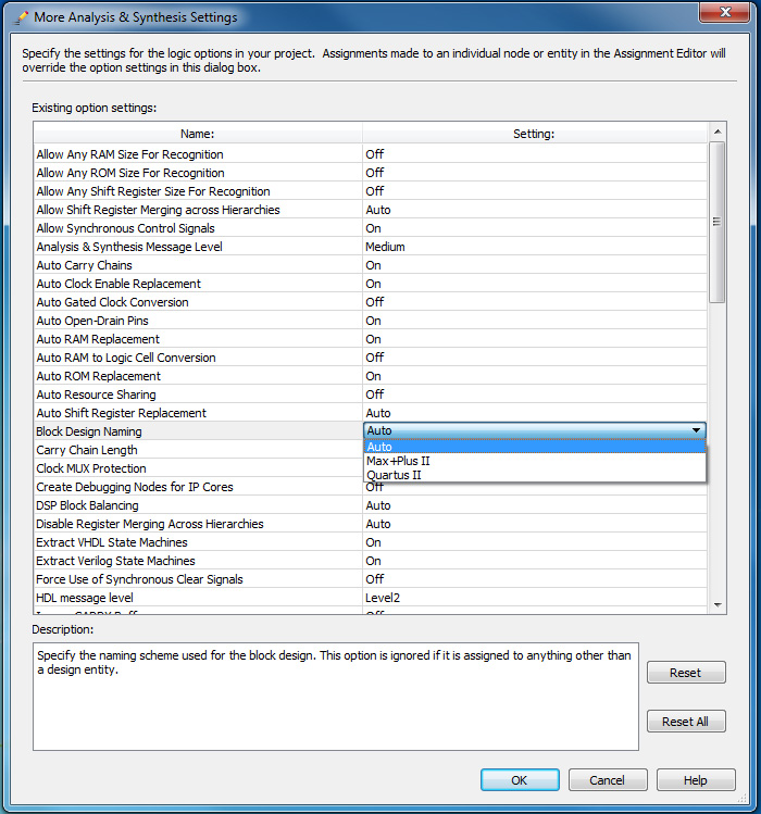
As can be seen from Figure 4, if you explicitly switch the renaming scheme to Quartus II, then the problem is solved.
Fig. 4 - Screenshot of Quartus II and photos from the oscilloscope
The way to solve the problem №2
If you start using the pins of the IDC connector in order (from 0 to n), then even with the Auto renaming scheme set, Quartus II will not rename anything.
Fig. 5 - Screenshot of Quartus II and photos from the oscilloscope
For clarity, the picture in the spoiler shows a photograph of the connectors:
PS I will be very happy if I can make life easier for someone and save his time.