Blender: 3D-model of the chip to connect to the library KiCad
- Tutorial
When designing printed circuit boards, it is often necessary to add a three-dimensional model of the electronic component to the board. But it is not always possible to find the finished file on the Internet. Drawing a model using the CAD-program of labor is not: to set the parameters of the body and the conclusions of the case of ten minutes, if, of course, you need an overall model and not a photorealistic picture.
But there is a problem: a professional CAD editor is not cheap, and free software is not always easy to use.
Fortunately, Blender can always come to the rescue. Yes, it is not intended to create drawings and exact models. But nevertheless, it allows you to quickly create three-dimensional models of electronic components for subsequent import into tracers. In this article I will describe how to create a chip model and connect it to the component library of KiCad.
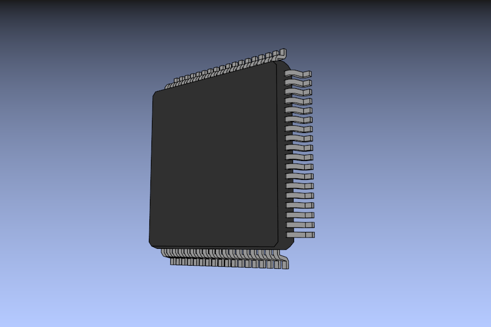
For example, let's draw a model of the microcontroller STM32F405xx in the LQFP64 package. All the necessary information for the work we take from the datasheet.

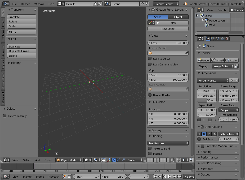
We start Blender and first remove all unnecessary components from the scene: the light, the cube and the camera. Select the object with the right mouse button and click "X". Or select all the objects with the button "A" and then "X".
For further work, we will need a side panel of settings, to call it, press "N". The window ready to work should look something like this:
For convenience, disable the perspective display mode - the number “5” on the additional keyboard.
The axes of coordinates in Blender and in KiCad do not coincide, so we will draw our chip so that its height coincides with the Y axis, and the length and width with the X and Z axes, respectively. Let's move to the right view by pressing the number "3" on the additional keyboard. If the 3D cursor is not in the center, the Shift + C key combination.
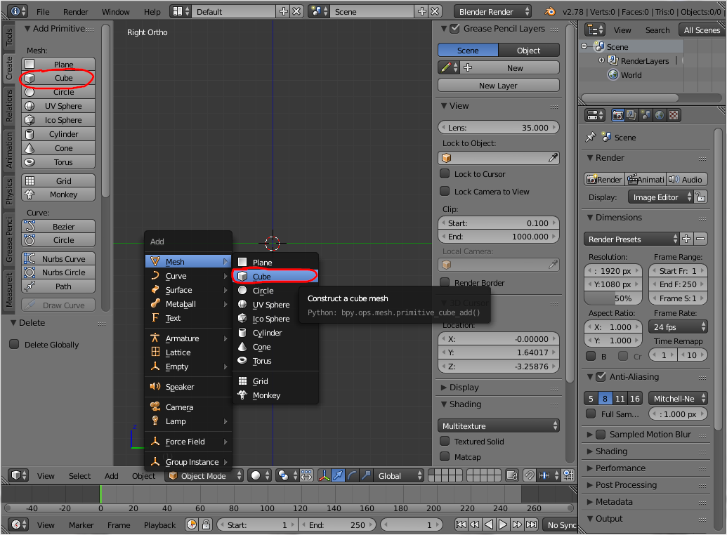
The body of the chip will create a cube. On the left in the Create panel, select the Cube shape. Or, using the Shift + A key combination, select Mesh → Cube from the drop-down menu.
The appeared cube is located in the center of the scene and has dimensions of 2x2x2 arbitrary units. This can be seen in the right sidebar (which we called by pressing the "N" key). If you now change the dimensions of the cube, then the scale of the figure will also change along with the size, which can lead to strange effects in the future. Therefore, we will reset the scaling: select the object and select it at the bottom in the panel Object → Apply → Scale (or Cntrl + A; S).
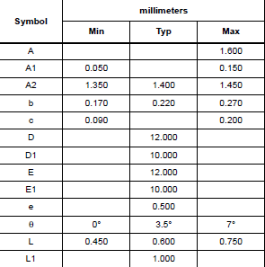
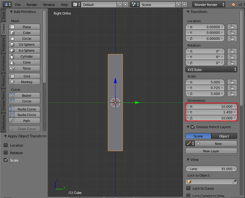
Now let's set the dimensions of the case. In the datasheet we find the length, width and height of the microcircuit case: 10 mm by 10 mm by 1.45 mm (max.). We use these numbers as our cube size. As mentioned above, the dimensions in X and Z are the length and width, and the size along the Y axis is the height.
The next step is to place the body at the correct height. To do this, go to the editing mode of the object (the button "Tab") and select the surface as an element of editing (face select). Then we select the top surface of the microcircuit - we have it on the right and press the key combination Shift + S → Cursor to selected:

Exit the edit mode with the button “Tab”. Next, in the Tools → Edit window, set the shape's anchor point using Set Origin → Origin to 3D Cursor.

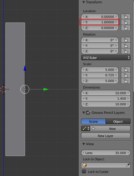
We see that now the position of the object along the Y axis has changed from zero to 0.725. Place the object so that the upper part of the case is offset by 1.6 mm relative to the origin - this is our maximum component height.
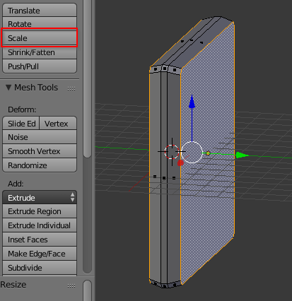
The dimensions of the case are correct. Now you can cosmetically improve the view by adding edges, as shown in pdf. The exact dimensions are not there, so let's do it by eye.
Switch to the edit mode (Tab key) and select the edge as the edit object (edge select). Holding the Shift key selects the four side edges of the object.

Apply the Bevel function to the selected elements - at the bottom select Mesh → Edges → Bevel, or press Cntrl + B. Next, either type a number on the keyboard (for example, 0.05), or by moving the mouse, select the desired chamfer size.

Now we will make bevels at the top and bottom of the chip of the chip, as shown in the side view of the chip.
To do this, in the edit mode, add a new edge: in the Tools → Loop Cut and Slide menu or with the Cntr + R combination. Place the edge as shown in the figure.

After clicking the right mouse button, the edge will automatically be located in the center of the shape. And we immediately apply the Bevel modifier to it, as we did with the side edges. Set the size to 0.2 (maximum size “c” in the drawing).
Now reduce the top and bottom surfaces of the chip. Turn on the surface editing mode (Face select) and select the top and bottom of the chip. The Scale modifier (the “S” key) is applicable to the two selected surfaces. Using the mouse on the eye, or by driving a certain number (for example, 0.96), we scale the selected surfaces.
We can say that the body of the chip is ready. It remains to attach 64 outputs to it. First, let's calculate the position of the first chip output. The size “E” (12 mm) in the drawing is divided in half and we get the external coordinate along the axis X = 12/2 = 6. The position along the axis Z in our case is equal to Z = 0.5 / 2 + 0.5 * 9 = 4.25
Before leaving the edit mode and removing the selection from the body, create a surface, which we transform into contact later. We turn to the right view (the number "3" on the additional keyboard). And then Create → Plane (Shift + A → Mesh → Plane). Let's turn it “face” to us: Align to View and set the calculated coordinates:

For further processing, reset the scaling and rotation of the shape: Object → Apply → Rotation and Scale. Or Cntrl + A → Rotation and Scale. (As in step 2). Now our surface will be set to the dimensions of the output in the section: width b = 0.27 mm (Z axis), height c = 0.2 mm (Y axis). And the Y displace it to a value of 0.1

is now "squeezed out" of the surface of the chip legs shape. Let us turn to the top view ("7" on the additional keyboard). Turn on the editing mode - “Tab” and select the created surface. Using Tools → Extrude → Region (or the “E” keys), then “X” (along the X axis), enter -0.6 from the keyboard and “Enter”. The number 0.6 we have corresponds to the size L in the drawing.
The color of the legs is different from the color of the microcircuit, because it turned out to be turned inside out. If you turn on the display of normals, you can see that they are all directed inward. Let's fix this: select the shape with the “A” key and in the Shaidng / UV → Normals panel, click Flip Direction. Now the figure is built correctly.

This procedure could have been avoided by turning the surface 180 degrees before the “extrusion” operation.
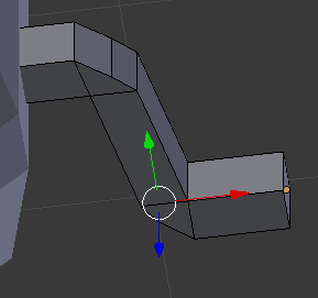
Create an additional edge on the chip output using the Tools → Loop Cut and Slide (or Cntrl + R) command and position it closer to the inner edge.

Select the top segment on the created surface and extrude it (the "E" key) up the "Y" coordinate to the middle of the chip.

We will shift the new surface slightly in the direction of the microcircuit: “G” - move, “X” - only along the X axis.

Perform the above operations for the top of the output. As a result, should get about the following picture.
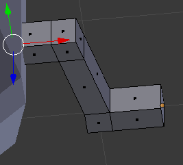
For beauty, let's move the corner edges, and get a pretty cute chip leg.
Using the Array modifier, create 18 pins of the microcircuit on one side. To begin with, reset the position and scale the output. Exit the “Tab” editing mode, select the foot, and apply Apply → Location, Rotation, Scale. It is necessary for the next modifier to correctly calculate the offset of the cloned objects.
Add Array modifier.

In the parameters of the modifier we set the number = 18, select the offset Constant, and the distance along the axis Z = -0.5

Received a number of conclusions. Create copies of them for the remaining three sides. To do this, remove the selection from all objects, set the 3D cursor in the center - Shift + C. And create an empty object - Shift + A → Empty → Plain Axes.

Now select the previously created chip output, and create the Array modifier again. Only this time we select Object offset, and the Empty-object created earlier. We specify the number of copies to be 4.
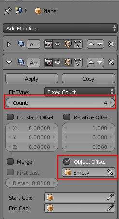
To position the created copies in the correct position, select the Empty object and rotate it about the Y axis by 90 degrees. The buttons "R" and "Y", then drive in the angle value "90".

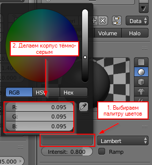
Let us paint our microchip for beauty and conclusions in different colors. Highlight the microcircuit case, and in the materials tab, create a new material:

And assign it a dark gray color: We
perform the same operation for the outputs of the microcircuit, but do the color a little bit brighter.
On this creation of the chip can be considered complete.
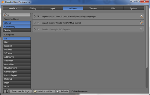
We export the model in vrml format. File → Export → VRML2. If there is no such menu, first go to File → User Preferences ... → Add-ons. In the search we drive in vrml and check the box opposite Import-Export VRML2 and Import-Export Web3D X3D / VRML2 format.
When exporting, we need to convert the units to inches. To do this, in the Scale field, enter the number 0.393701 (1 mm / 2.54 inch = 0.393701).

That's all, the chip model is ready.
We create a landing area in the library and connect a three-dimensional model. If everything was done correctly in the previous steps, then the model should immediately “lie down” in its place.
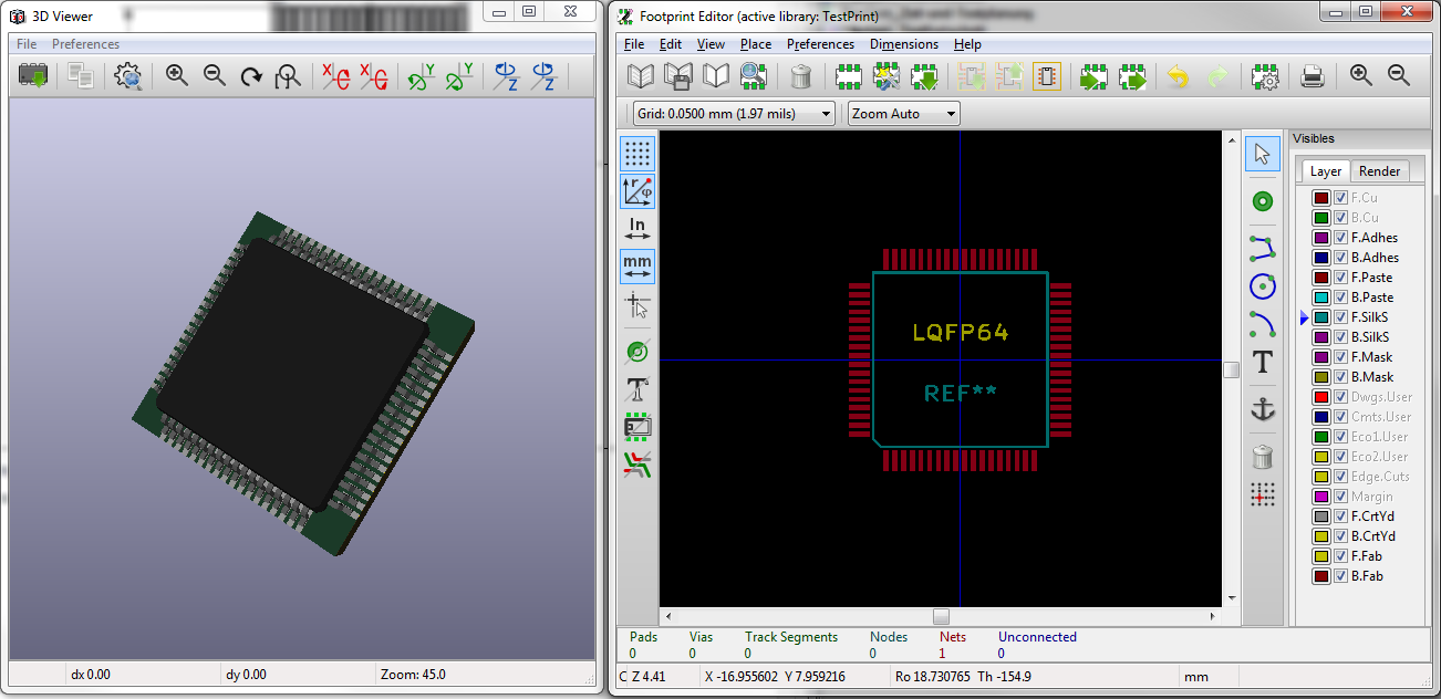
The microcircuit created by this method can be used for visual control of the landing pad.
But there is a problem: a professional CAD editor is not cheap, and free software is not always easy to use.
Fortunately, Blender can always come to the rescue. Yes, it is not intended to create drawings and exact models. But nevertheless, it allows you to quickly create three-dimensional models of electronic components for subsequent import into tracers. In this article I will describe how to create a chip model and connect it to the component library of KiCad.
For example, let's draw a model of the microcontroller STM32F405xx in the LQFP64 package. All the necessary information for the work we take from the datasheet.
1. Preparing Blender
We start Blender and first remove all unnecessary components from the scene: the light, the cube and the camera. Select the object with the right mouse button and click "X". Or select all the objects with the button "A" and then "X".
For further work, we will need a side panel of settings, to call it, press "N". The window ready to work should look something like this:
For convenience, disable the perspective display mode - the number “5” on the additional keyboard.
The axes of coordinates in Blender and in KiCad do not coincide, so we will draw our chip so that its height coincides with the Y axis, and the length and width with the X and Z axes, respectively. Let's move to the right view by pressing the number "3" on the additional keyboard. If the 3D cursor is not in the center, the Shift + C key combination.
2. We create the body of the chip
The body of the chip will create a cube. On the left in the Create panel, select the Cube shape. Or, using the Shift + A key combination, select Mesh → Cube from the drop-down menu.
The appeared cube is located in the center of the scene and has dimensions of 2x2x2 arbitrary units. This can be seen in the right sidebar (which we called by pressing the "N" key). If you now change the dimensions of the cube, then the scale of the figure will also change along with the size, which can lead to strange effects in the future. Therefore, we will reset the scaling: select the object and select it at the bottom in the panel Object → Apply → Scale (or Cntrl + A; S).
3. Set the size of the chip
Now let's set the dimensions of the case. In the datasheet we find the length, width and height of the microcircuit case: 10 mm by 10 mm by 1.45 mm (max.). We use these numbers as our cube size. As mentioned above, the dimensions in X and Z are the length and width, and the size along the Y axis is the height.
4. Place the microcircuit case
The next step is to place the body at the correct height. To do this, go to the editing mode of the object (the button "Tab") and select the surface as an element of editing (face select). Then we select the top surface of the microcircuit - we have it on the right and press the key combination Shift + S → Cursor to selected:
Exit the edit mode with the button “Tab”. Next, in the Tools → Edit window, set the shape's anchor point using Set Origin → Origin to 3D Cursor.
We see that now the position of the object along the Y axis has changed from zero to 0.725. Place the object so that the upper part of the case is offset by 1.6 mm relative to the origin - this is our maximum component height.
5. Add ribs
The dimensions of the case are correct. Now you can cosmetically improve the view by adding edges, as shown in pdf. The exact dimensions are not there, so let's do it by eye.
Switch to the edit mode (Tab key) and select the edge as the edit object (edge select). Holding the Shift key selects the four side edges of the object.
Apply the Bevel function to the selected elements - at the bottom select Mesh → Edges → Bevel, or press Cntrl + B. Next, either type a number on the keyboard (for example, 0.05), or by moving the mouse, select the desired chamfer size.
Now we will make bevels at the top and bottom of the chip of the chip, as shown in the side view of the chip.
To do this, in the edit mode, add a new edge: in the Tools → Loop Cut and Slide menu or with the Cntr + R combination. Place the edge as shown in the figure.
After clicking the right mouse button, the edge will automatically be located in the center of the shape. And we immediately apply the Bevel modifier to it, as we did with the side edges. Set the size to 0.2 (maximum size “c” in the drawing).
Now reduce the top and bottom surfaces of the chip. Turn on the surface editing mode (Face select) and select the top and bottom of the chip. The Scale modifier (the “S” key) is applicable to the two selected surfaces. Using the mouse on the eye, or by driving a certain number (for example, 0.96), we scale the selected surfaces.
6. Create the first output
We can say that the body of the chip is ready. It remains to attach 64 outputs to it. First, let's calculate the position of the first chip output. The size “E” (12 mm) in the drawing is divided in half and we get the external coordinate along the axis X = 12/2 = 6. The position along the axis Z in our case is equal to Z = 0.5 / 2 + 0.5 * 9 = 4.25
Before leaving the edit mode and removing the selection from the body, create a surface, which we transform into contact later. We turn to the right view (the number "3" on the additional keyboard). And then Create → Plane (Shift + A → Mesh → Plane). Let's turn it “face” to us: Align to View and set the calculated coordinates:
For further processing, reset the scaling and rotation of the shape: Object → Apply → Rotation and Scale. Or Cntrl + A → Rotation and Scale. (As in step 2). Now our surface will be set to the dimensions of the output in the section: width b = 0.27 mm (Z axis), height c = 0.2 mm (Y axis). And the Y displace it to a value of 0.1
is now "squeezed out" of the surface of the chip legs shape. Let us turn to the top view ("7" on the additional keyboard). Turn on the editing mode - “Tab” and select the created surface. Using Tools → Extrude → Region (or the “E” keys), then “X” (along the X axis), enter -0.6 from the keyboard and “Enter”. The number 0.6 we have corresponds to the size L in the drawing.
The color of the legs is different from the color of the microcircuit, because it turned out to be turned inside out. If you turn on the display of normals, you can see that they are all directed inward. Let's fix this: select the shape with the “A” key and in the Shaidng / UV → Normals panel, click Flip Direction. Now the figure is built correctly.
This procedure could have been avoided by turning the surface 180 degrees before the “extrusion” operation.
Create an additional edge on the chip output using the Tools → Loop Cut and Slide (or Cntrl + R) command and position it closer to the inner edge.
Select the top segment on the created surface and extrude it (the "E" key) up the "Y" coordinate to the middle of the chip.
We will shift the new surface slightly in the direction of the microcircuit: “G” - move, “X” - only along the X axis.
Perform the above operations for the top of the output. As a result, should get about the following picture.
For beauty, let's move the corner edges, and get a pretty cute chip leg.
7. Clone chip output
Using the Array modifier, create 18 pins of the microcircuit on one side. To begin with, reset the position and scale the output. Exit the “Tab” editing mode, select the foot, and apply Apply → Location, Rotation, Scale. It is necessary for the next modifier to correctly calculate the offset of the cloned objects.
Add Array modifier.
In the parameters of the modifier we set the number = 18, select the offset Constant, and the distance along the axis Z = -0.5
Received a number of conclusions. Create copies of them for the remaining three sides. To do this, remove the selection from all objects, set the 3D cursor in the center - Shift + C. And create an empty object - Shift + A → Empty → Plain Axes.
Now select the previously created chip output, and create the Array modifier again. Only this time we select Object offset, and the Empty-object created earlier. We specify the number of copies to be 4.
To position the created copies in the correct position, select the Empty object and rotate it about the Y axis by 90 degrees. The buttons "R" and "Y", then drive in the angle value "90".
8. Chip color
Let us paint our microchip for beauty and conclusions in different colors. Highlight the microcircuit case, and in the materials tab, create a new material:
And assign it a dark gray color: We
perform the same operation for the outputs of the microcircuit, but do the color a little bit brighter.
On this creation of the chip can be considered complete.
9. Export the resulting model to KiCad.
We export the model in vrml format. File → Export → VRML2. If there is no such menu, first go to File → User Preferences ... → Add-ons. In the search we drive in vrml and check the box opposite Import-Export VRML2 and Import-Export Web3D X3D / VRML2 format.
When exporting, we need to convert the units to inches. To do this, in the Scale field, enter the number 0.393701 (1 mm / 2.54 inch = 0.393701).
That's all, the chip model is ready.
10. Connecting the model to KiCad
We create a landing area in the library and connect a three-dimensional model. If everything was done correctly in the previous steps, then the model should immediately “lie down” in its place.
The microcircuit created by this method can be used for visual control of the landing pad.