7 rules for the design of printed circuit boards
Greetings In the process of discussing the article by Comrade KSVl , the need for a small manual on the design of printed circuit boards was voiced. Very often on Habré, I see articles in the style of "5 rules of code design" or "5 steps to a successful project", that is, very convenient abstracts on a specific topic. Unfortunately, there are few such articles on the development of electronics and this is bad ...
I promised the user KSVl and some other readers an article with the basic principles of designing printed circuit boards (PP), I also invite all fans to get acquainted with a cup of coffee to get acquainted!
All the rules described in the article are the most basic and are aimed exclusively at very beginner developers for whom electronics is just a hobby. At once I want to note that this article does not claim to be absolute truth and all explanations are given in free form.
Surely there are people who will say: "Yes, and so it works, why change something?". And here, alas, I am not ready to waste energy and persuade you. Some want to do everything well, efficiently and reliably, while others cannot understand this desire.
Sources of information on which the rules described in the article are based:
Error - very often novice developers use the same width of conductors (tracks), which is the default in the used CAD. In the article mentioned earlier, the author used EasyEDA and there the base width is 6 mils, that is, about 0.15 mm. This width of conductors is used almost everywhere and this is bad, because it leads to a number of problems.
Problem number 1 - voltage drop. We all remember Ohm's law from which it follows that the smaller the sectional area of the conductor, the greater its resistance. The greater the resistance of the conductor, the more voltage will drop on it.
Problem number 2- heating conductor. Here is the same Ohm's law, the power allocated to the conductor is proportional to its resistance, that is, the greater the resistance, the more heat is released on the conductor. Road 0.15 mm current in 5-10A easily evaporates.
Problem number 3 - spurious inductance. This moment to the base is hardly already relevant, but you need to know about it. The smaller the conductor cross section, the greater its inductance. That is, any conductor is actually not just a “piece of copper,” it is a component of resistance, inductance, and parasitic capacitance. If these parameters are too high, then they begin to negatively affect the operation of the circuit. More often they appear at frequencies greater than 10 MHz, for example, when working with SPI.
Problem number 4- low mechanical strength. I think it is not necessary to explain that the 2 mm wide track is more firmly attached to the textolite base than the 0.15 mm track. For the sake of interest, take the factory unnecessary fee and pick it up.
The solution is to use the maximum possible conductor width. If the conductor can be drawn with a width of 0.6 mm, then it is better than holding it with a width of 0.15 mm.
Example:
1) Bad
2) Good
The pins imply the pad of the component (pad), vias (via) and other objects that we connect on the board with the help of conductors (tracks).
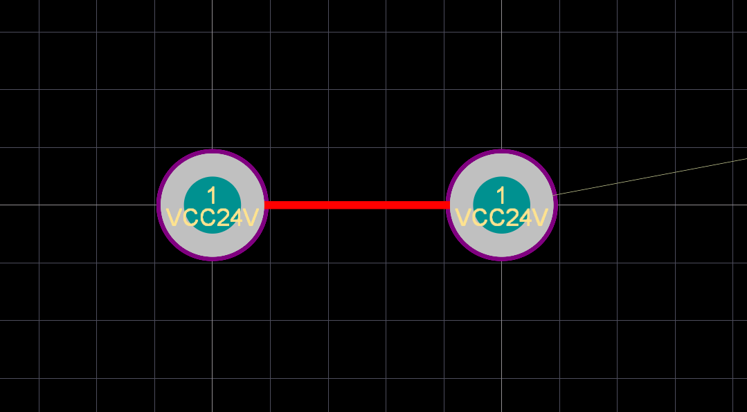
Error - there are two extremes. In one, the developer makes a mistake from rule No. 1 and connects a 0.15 mm track to the smd pin of resistor 1206. In another case, on the contrary, uses a conductor whose width is equal to the width of the contact pad. Both options are bad.
Problem number 1 - low mechanical strength. If several attempts are made to solder a component, the pad or track will simply be peeled off from the textolite base of the printed circuit board.
Problem number 2- technological problems with the installation of the board. Although this will become a problem if you start ordering in China not only the board, but also the assembly. Of course you will collect, but% of marriage grows.
The solution - the width of the conductor connected to the contact pad should be approximately 80% of the width of this pad.
Example:
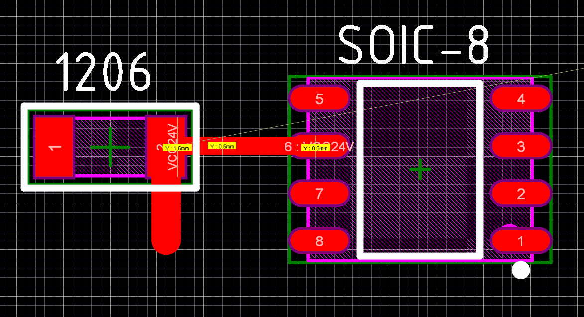
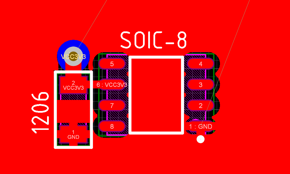
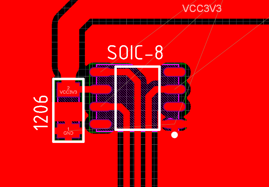
1) Bad 2) Good The size of the pad of a capacitor 1206 in this case is 1.6 x 1 mm . Accordingly, a track equal to 80% of the pad width, i.e. 0.8 mm (80% of 1 mm), is used to sum the signal from below. To sum the signal to the right, a track 1.2 mm thick is used (approximately 80% of 1.6 mm). The width of the area of the microcircuit in the SOIC-8 package is 0.6 mm, so you need to sum up the signal using a track of about 0.5 mm.
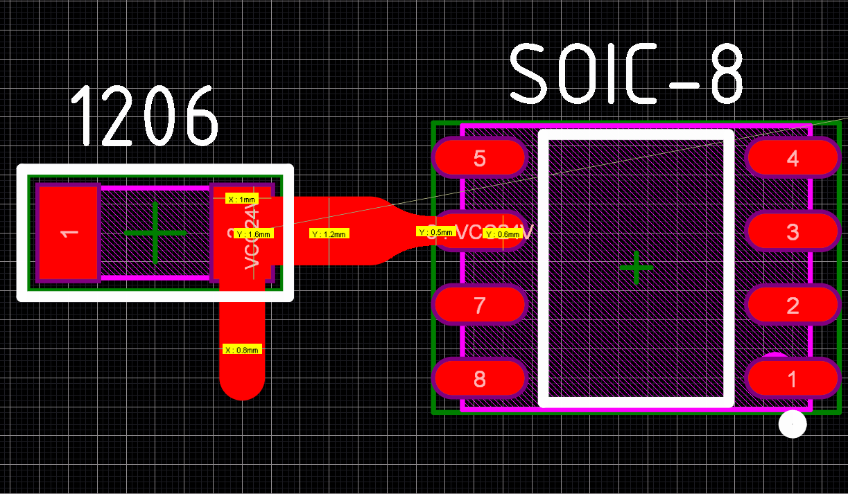
It should be understood that this option is ideal. The transition from 1.2 mm to 0.5 mm you probably will not like - the extra fuss. It can be avoided. To do this, usually take the width of the track relative to the minimum pad-a (pad), that is, in this case, you can do this: As you can see, I chose the width of the conductor on the minimum pad, that is, on the chip output area in the SOIC-8 package. Such a simplification is permissible, but it should be applied wisely.
Now consider the case when the simplification in relation to the rule number 2 is simply unacceptable, namely - the design of power circuits. This rule is based on the previous two and is a particular, but perhaps the most critical case.
Error - disregard of rules №1 and №2 when designing power circuits.
Problem number 1 - at the output of your voltage regulator strictly + 3.3V. You turn on the device and observe that the chip behaves inadequately, the ADC measures not exactly and periodically turns off. You measure the voltage on the legs of the consumer (microchips) and find instead of + 3.3V only + 2.6V.
Problem # 2 - your DC-DC converter does not start, or the output has large ripple.
Problem number 3- in attempts to find a fault, you put the oscilloscope probe on the + 3.3V line and find there, instead of a constant voltage, some terrible pulsations and interferences.
The solution - we strictly observe rules No. 1 and No. 2 strictly and fanatically. The tracks are as wide as possible. Power should come to the microcircuit through a ceramic capacitor, which if possible is placed closer to the output of this microcircuit.
Example:
1) Bad 2) Good. What I did to make it good: 1) The power track of the VCC3V3 is no longer suitable for bypassing the capacitor, but through it. That is, first to the capacitor, and then to the output of the microcircuit

2) I have used a bore (via) 1.2 / 0.6 mm. Yes, according to the requirements for accuracy class 4 (standard), I can use a bore of 0.7 / 0.3 mm, but did not do this and applied a more dimensional transition. This made it possible to reduce its resistance and skip more current
3) The power bus that comes from the stabilizer I now have not 0.3 mm, but 2 mm! Do not be afraid to make wide conductors. This approach minimizes the voltage drop in the circuit and reduces the inductance of the conductor.
The influence of the quality of the earth bus design (GND) can be talked about forever, but any conversation boils down to a simple fact: it is stable and the device’s performance depends most of all on the design of the earth . This problem is very voluminous and requires in-depth study, so I will give the most basic recommendations.
Error - tracing the GND circuit (ground) as a normal conductor, and even the minimum width. This is just a k-to-combo!
Problem number 1 - the instability of the device and strong interference in the circuits, especially in power circuits.
Problem number 2 - heating and often a thin conductor break, as it has a large current.
Decision- use a polygon for distributing the GND circuit, and ideally a separate layer that is completely allocated for this circuit, for example, the lower layer.
Example:
1) Bad 2) Good As you can see, instead of the usual conductor I applied a fill with a solid polygon. This solution provided me with a huge cross-sectional area, because the landfill is just a very large conductor. Only sometimes such a solution has a disadvantage, for example, when mounting density is high and other conductors break a solid polygon, as LED1.3 circuits here break the shortest path between the output of the microcircuit and the capacitor (GND): A separate layer of GND mentioned above will help us. Ideally, in a two-layer board, select the bottom layer under it, and in the multilayer board, one of the inner layers:

Thus, we restored the shortest path for the current along the GND circuit, and in this case the lower layer (blue color), which completely represents the earthen polygon, helped. Vias (via) near the contact pads provided for them the shortest possible connection to the lower layer of earth.
Of course, this is an ideal case and sometimes it will not be possible to implement it without increasing the cost of the board, so the decision is yours. Sometimes "super" reliability is not needed, it is important to find here a middle ground between cost and quality.
The minimum value of the gap between the copper conductors on the printed circuit board, we dictate the technological requirements. For the 4th (standard) class, the value is 0.15 / 0.15 mm or 6/6 mils. The maximum width is limited only by your imagination, board dimensions and common sense.
Error - the gap is not large enough, usually leave the default value of about 0.15 mm.
Problem number 1 - electrical breakdown. A short circuit occurs when 2 conductors with different potential are closed, for example, with a metal object and the current rises sharply. Unfortunately, there are no perfect dielectric materials, and at some point any material begins to conduct. An example of this is insulators on power lines, and sometimes even punches them. This phenomenon occurs when the value is exceeded.critical breakdown voltage . For the same reason, fiberglass, which is the main part of the printed circuit boards, at some point may begin to pass current.
The solution is to increase the distance between the conductors. The breakdown voltage depends on the type of material and the thickness / width of the insulator. In the case of printed circuit boards, the distance (gap) between conductors is precisely the parameter that affects the critical value of the breakdown voltage. The greater the distance between the conductors, the greater the voltage needed to penetrate it .
Just want to say that the breakdown of fiberglass is not always the most urgent problem. The air that surrounds the board is also a dielectric, but under certain conditions it becomes a conductor, remember a thunderstorm. Air electrical breakdown is a big problem in electronics, especially considering that the air can be dry, and it can also have a humidity of 90-100%, for example, in the tropics or in the North.
Example:
Let's agree that in this example there are 3 conductors: rectified mains voltage + 310V, low-voltage power line for the microcontroller + 3.3V and earth bus (GND).
1) Bad 2) Good Why 0.3 mm is bad, and 0.8 mm is already good you ask and I will give you 2 sources as an answer:
1) Ordinary physics and electrical engineering. The data in them varies due to different measurement methods and other things, but the most realistic figure for dry air is 2 kV / mm . Here many people will be frightened by the numbers and will think: “I don’t have such voltages” and this will be a mistake. This value is typical only for dry air, which is rarely possible to meet in real conditions. And here the numbers are much more modest, for example, at a humidity of 100%, the air breakdown voltage is only 250 V / mm ! And the value of the breakdown voltage is influenced by the dustiness of the air and the board, as well as the atmospheric pressure (the curve and the Paschen law).
2) IPC-2221 standard, the link to which I gave at the beginning. We are interested in the table 6-1, which looks like this:
As you can see in the table for a large number of values, even for our particular case, 301-500V . If we look, we will see a value of 0.25 mm for closed conductors on the inner layers, that is, in “ideal” conditions without access of dust, dirt and moisture. If the device works somewhere in the mountains and the conductor is on the outer layers (all conductors in the case of a 2-layer board) at an altitude of 3000 meters, then there is a minimum gap of 2.5 mm, that is, 10 times more. If we operate the device at a higher height, then the gap is needed as early as 12.5 mm! It is worth making a remark - such a large gap is required if our board is not covered with protective compounds, for example, varnish or compound. As soon as a protective coating appears, we see already more adequate values: 0.8 and1.5 mm.
Therefore, in the “good” example, in addition to ensuring a gap of 0.8 mm, it is also necessary to cover the board with a protective compound, for example, varnish after the device has been installed, washed and dried. Otherwise it is necessary to increase the gap!
Error - equating the dielectric gap to galvanic. In fact, they are very similar, but the requirements are stricter when it comes to galvanic isolation. A striking case is the decoupling of the control circuit and the power section using a relay or an optocoupler, when the gap between the decoupled sides is also chosen to be 0.8 or 1.5 mm.
Problem number 1 - insulation breakdown, failure of the control system and other expensive equipment.
Decision- increase the threshold electrical breakdown. Standard values are typically 1.5 kV, 2.5 kV and 4 kV. If your device works with mains voltage, but the person does not interact with it directly, then an isolation voltage of 1.5 kV will be sufficient. If a person is supposed to interact with the device, for example, through buttons and other controls, I recommend using insulation with a voltage of 2.5 kV or more.
Example:
1) Bad
What is wrong you ask, because there are gaps on the board, they can be made and 1.5 mm. The fact is that even if you make a gap of 2 mm, then this will not be enough to provide insulation. The “weakest” place should be the distance between the relay control terminals (1-2) and the power terminals (3-8). It is also necessary to take into account that the breakdown can be not only between conductors on the same layer, but also on different ones - through the board through fiberglass laminate.
2) Good What was done to improve the situation: a) There was a clear boundary between the low-voltage and high-voltage parts. Now the conductor + 3.3V does not pass in the high-voltage region + 310V, the GND test range does not go beyond the low-voltage part, respectively, and there will be no breakdown. Also, there should be nothing at all in the zone / boundary of the galvanic isolation.
b) The isolation zone is freed from the solder mask. The mask is also a weak point and, depending on the quality, will break through it before the glass fiber laminate. It is not necessary to do this in the general case, but if people interact with the device, I highly recommend it.
c) As I wrote above, the weak point is the distance between the control and power outputs of the relay. Everywhere I was able to make an insulating zone of 4 mm, and here only 2.5 mm. We cleared the mask, from the conductors, too, and the only thing that can breakdown on the board can happen is fiberglass laminate. Therefore, we remove it, I made a cutout under the 2.5 mm wide relay and removed the textolite between the leads. This operation is also not required, but it significantly increases the reliability and safety of your device.
Error - I often observe a picture when on a 2-layer printed circuit board in order to connect 2 pads, I use 3..4 ... or even 5 vias.
Problem number 1 - vias (via) becomes too much on the board and this limits the space for conductors, which leads to lengthening of the chains, and consequently to an increase in their resistance. Reduces the stability of circuits and interference signals.
Decision- use the minimum number of vias: if you need to connect 2 contacts on different layers, then do not use more than 1 vias. If 2 pins are on the same layer and you cannot connect them directly, then use a maximum of 2 vias. If you need more transitions to connect, then something you are doing wrong - train the logic and re-divide the section of the board that led to the problem.
Example:
1) Bad 2) Good The minimum number of vias (via) was used for the connection, which gives more space for other conductors and provides the minimum parasitic parameters of the conductor.
I hope this article will be useful for beginners electronics and save them at least from the most simple errors. I think quite a few people in these rules will see their shortcomings, but you should not blindly copy from this rule. Always think with your head and look for the best option, sometimes 4 vias for the 1st chain are acceptable, if it allows you to improve the final result.
Those who are not satisfied with this material - I propose to familiarize themselves with the IPC standards diagonally, it makes no sense to read much, as well as to read the initial course of “black magic” from Howard Jones. It also includes the physical design principles, as well as many recommendations on the design of standard circuits and interfaces. It used to be high-speed digital circuits that were something magical and sublime, but today even 2018 are in the courtyard of 2018 and even beginners are facing them, for example, when connecting sensors and memory via SPI or displays.
I promised the user KSVl and some other readers an article with the basic principles of designing printed circuit boards (PP), I also invite all fans to get acquainted with a cup of coffee to get acquainted!
Prologue
All the rules described in the article are the most basic and are aimed exclusively at very beginner developers for whom electronics is just a hobby. At once I want to note that this article does not claim to be absolute truth and all explanations are given in free form.
Surely there are people who will say: "Yes, and so it works, why change something?". And here, alas, I am not ready to waste energy and persuade you. Some want to do everything well, efficiently and reliably, while others cannot understand this desire.
Sources of information on which the rules described in the article are based:
- The course of general physics and electrical engineering. All within the 1st year of university
- Books by Howard Jones "Designing high-speed digital devices: the initial course of black magic" and "High-speed transfer of digital data: the highest course of black magic"
- IPC standards, for example, IPC-2221A. There is a translation in Russian (old version) and the original of the latest versions in English
- Own experience
Rule # 1 - Conductor Width
Error - very often novice developers use the same width of conductors (tracks), which is the default in the used CAD. In the article mentioned earlier, the author used EasyEDA and there the base width is 6 mils, that is, about 0.15 mm. This width of conductors is used almost everywhere and this is bad, because it leads to a number of problems.
Problem number 1 - voltage drop. We all remember Ohm's law from which it follows that the smaller the sectional area of the conductor, the greater its resistance. The greater the resistance of the conductor, the more voltage will drop on it.
Problem number 2- heating conductor. Here is the same Ohm's law, the power allocated to the conductor is proportional to its resistance, that is, the greater the resistance, the more heat is released on the conductor. Road 0.15 mm current in 5-10A easily evaporates.
Problem number 3 - spurious inductance. This moment to the base is hardly already relevant, but you need to know about it. The smaller the conductor cross section, the greater its inductance. That is, any conductor is actually not just a “piece of copper,” it is a component of resistance, inductance, and parasitic capacitance. If these parameters are too high, then they begin to negatively affect the operation of the circuit. More often they appear at frequencies greater than 10 MHz, for example, when working with SPI.
Problem number 4- low mechanical strength. I think it is not necessary to explain that the 2 mm wide track is more firmly attached to the textolite base than the 0.15 mm track. For the sake of interest, take the factory unnecessary fee and pick it up.
The solution is to use the maximum possible conductor width. If the conductor can be drawn with a width of 0.6 mm, then it is better than holding it with a width of 0.15 mm.
Example:
1) Bad
2) Good
Rule number 2 - Connect to pins
The pins imply the pad of the component (pad), vias (via) and other objects that we connect on the board with the help of conductors (tracks).
Error - there are two extremes. In one, the developer makes a mistake from rule No. 1 and connects a 0.15 mm track to the smd pin of resistor 1206. In another case, on the contrary, uses a conductor whose width is equal to the width of the contact pad. Both options are bad.
Problem number 1 - low mechanical strength. If several attempts are made to solder a component, the pad or track will simply be peeled off from the textolite base of the printed circuit board.
Problem number 2- technological problems with the installation of the board. Although this will become a problem if you start ordering in China not only the board, but also the assembly. Of course you will collect, but% of marriage grows.
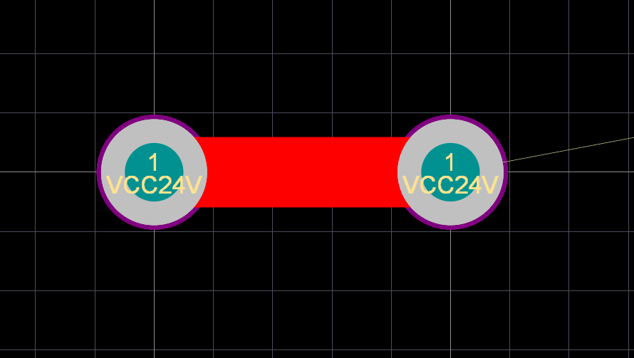
The solution - the width of the conductor connected to the contact pad should be approximately 80% of the width of this pad.
Example:
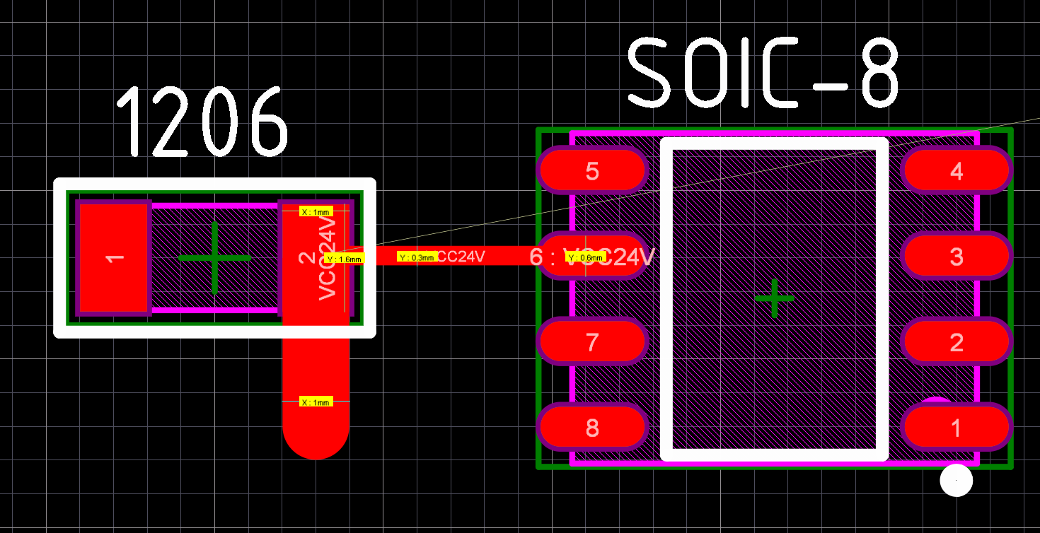
1) Bad 2) Good The size of the pad of a capacitor 1206 in this case is 1.6 x 1 mm . Accordingly, a track equal to 80% of the pad width, i.e. 0.8 mm (80% of 1 mm), is used to sum the signal from below. To sum the signal to the right, a track 1.2 mm thick is used (approximately 80% of 1.6 mm). The width of the area of the microcircuit in the SOIC-8 package is 0.6 mm, so you need to sum up the signal using a track of about 0.5 mm.
It should be understood that this option is ideal. The transition from 1.2 mm to 0.5 mm you probably will not like - the extra fuss. It can be avoided. To do this, usually take the width of the track relative to the minimum pad-a (pad), that is, in this case, you can do this: As you can see, I chose the width of the conductor on the minimum pad, that is, on the chip output area in the SOIC-8 package. Such a simplification is permissible, but it should be applied wisely.
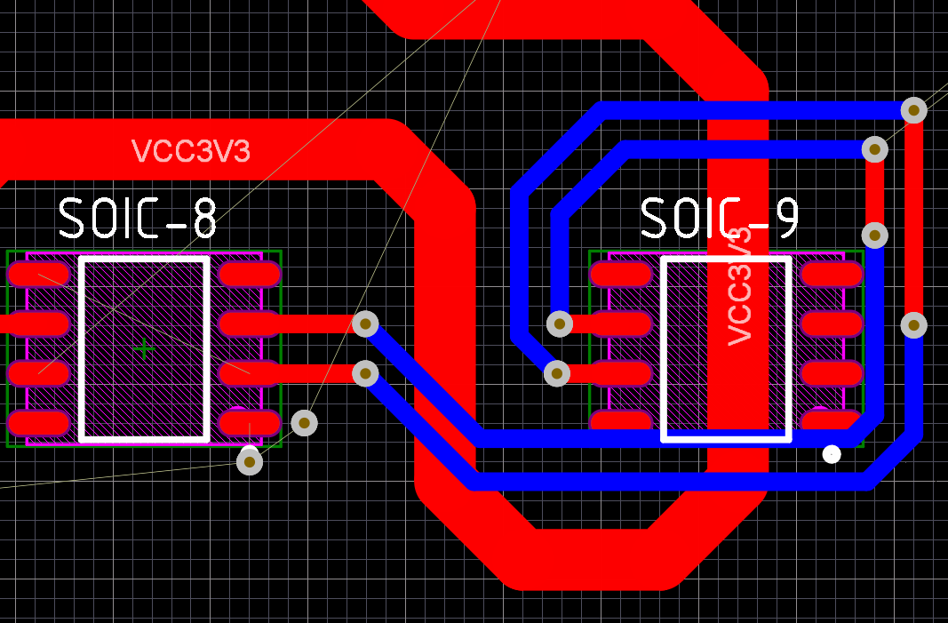
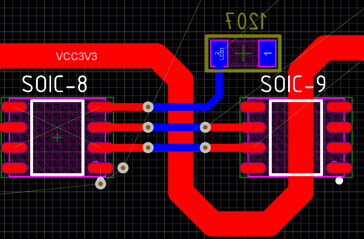
Rule number 3 - Power Chains
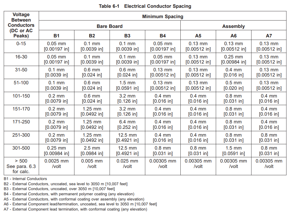
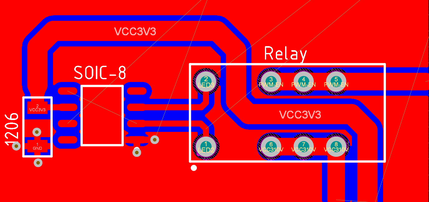
Now consider the case when the simplification in relation to the rule number 2 is simply unacceptable, namely - the design of power circuits. This rule is based on the previous two and is a particular, but perhaps the most critical case.
Error - disregard of rules №1 and №2 when designing power circuits.
Problem number 1 - at the output of your voltage regulator strictly + 3.3V. You turn on the device and observe that the chip behaves inadequately, the ADC measures not exactly and periodically turns off. You measure the voltage on the legs of the consumer (microchips) and find instead of + 3.3V only + 2.6V.
Problem # 2 - your DC-DC converter does not start, or the output has large ripple.
Problem number 3- in attempts to find a fault, you put the oscilloscope probe on the + 3.3V line and find there, instead of a constant voltage, some terrible pulsations and interferences.
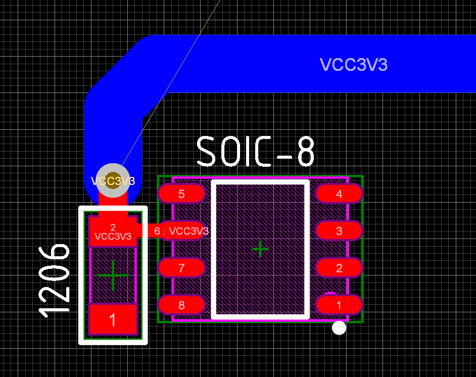
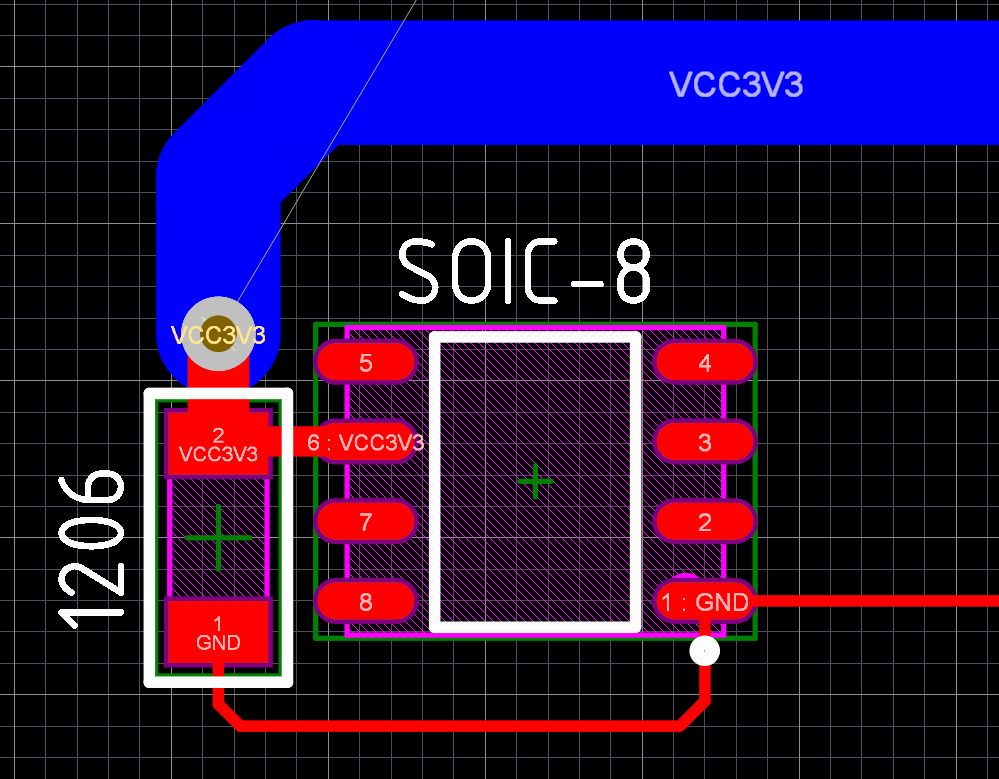
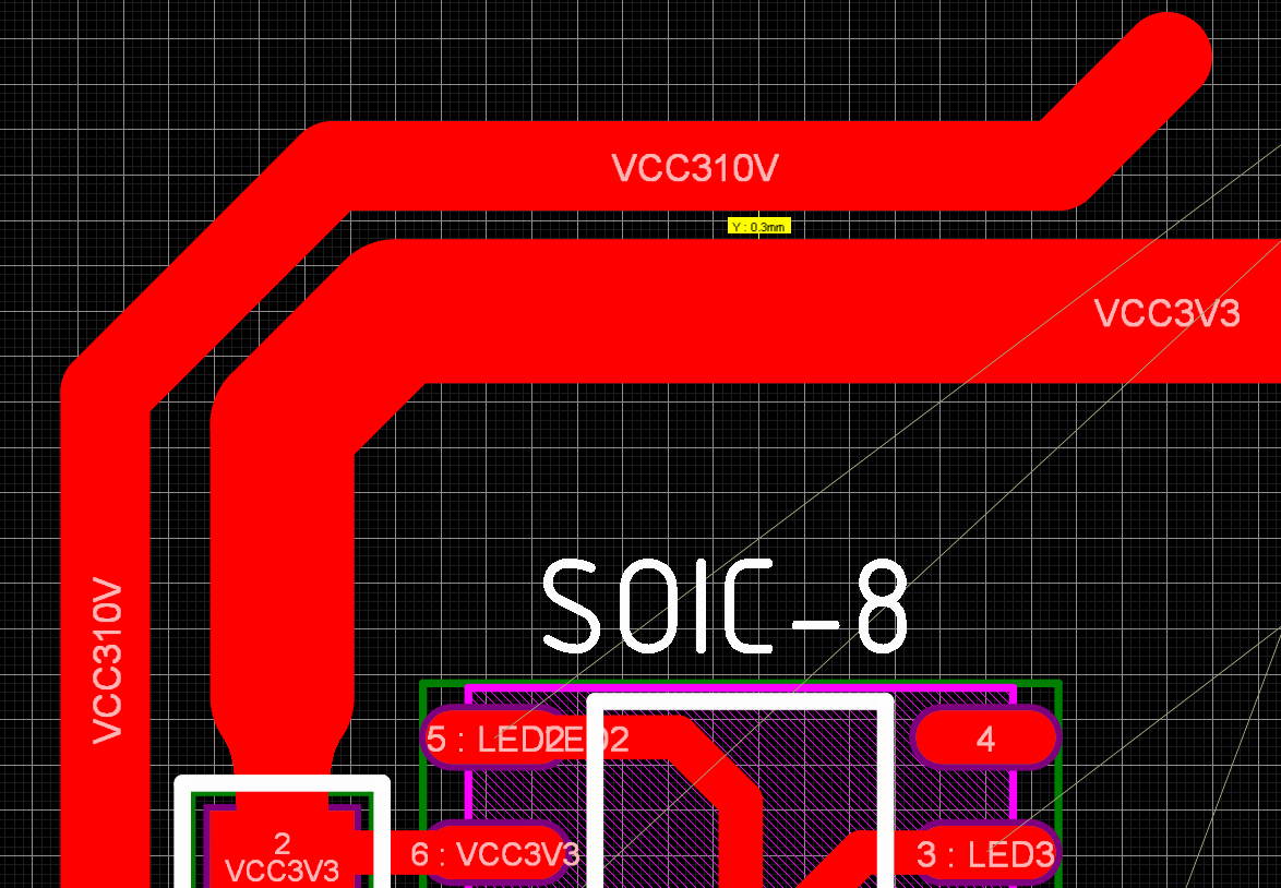
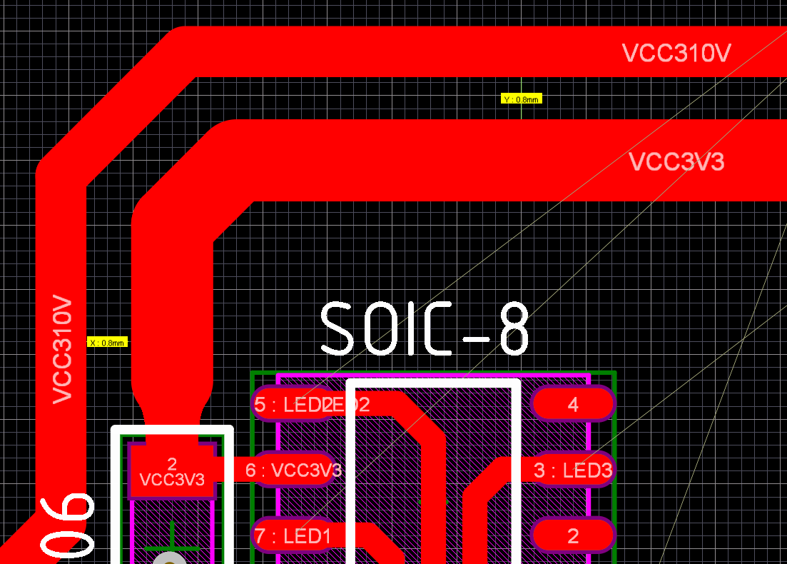
The solution - we strictly observe rules No. 1 and No. 2 strictly and fanatically. The tracks are as wide as possible. Power should come to the microcircuit through a ceramic capacitor, which if possible is placed closer to the output of this microcircuit.
Example:
1) Bad 2) Good. What I did to make it good: 1) The power track of the VCC3V3 is no longer suitable for bypassing the capacitor, but through it. That is, first to the capacitor, and then to the output of the microcircuit
2) I have used a bore (via) 1.2 / 0.6 mm. Yes, according to the requirements for accuracy class 4 (standard), I can use a bore of 0.7 / 0.3 mm, but did not do this and applied a more dimensional transition. This made it possible to reduce its resistance and skip more current
3) The power bus that comes from the stabilizer I now have not 0.3 mm, but 2 mm! Do not be afraid to make wide conductors. This approach minimizes the voltage drop in the circuit and reduces the inductance of the conductor.
Rule number 4 - Earth
The influence of the quality of the earth bus design (GND) can be talked about forever, but any conversation boils down to a simple fact: it is stable and the device’s performance depends most of all on the design of the earth . This problem is very voluminous and requires in-depth study, so I will give the most basic recommendations.
Error - tracing the GND circuit (ground) as a normal conductor, and even the minimum width. This is just a k-to-combo!
Problem number 1 - the instability of the device and strong interference in the circuits, especially in power circuits.
Problem number 2 - heating and often a thin conductor break, as it has a large current.
Decision- use a polygon for distributing the GND circuit, and ideally a separate layer that is completely allocated for this circuit, for example, the lower layer.
Example:
1) Bad 2) Good As you can see, instead of the usual conductor I applied a fill with a solid polygon. This solution provided me with a huge cross-sectional area, because the landfill is just a very large conductor. Only sometimes such a solution has a disadvantage, for example, when mounting density is high and other conductors break a solid polygon, as LED1.3 circuits here break the shortest path between the output of the microcircuit and the capacitor (GND): A separate layer of GND mentioned above will help us. Ideally, in a two-layer board, select the bottom layer under it, and in the multilayer board, one of the inner layers:
Thus, we restored the shortest path for the current along the GND circuit, and in this case the lower layer (blue color), which completely represents the earthen polygon, helped. Vias (via) near the contact pads provided for them the shortest possible connection to the lower layer of earth.
Of course, this is an ideal case and sometimes it will not be possible to implement it without increasing the cost of the board, so the decision is yours. Sometimes "super" reliability is not needed, it is important to find here a middle ground between cost and quality.
Rule number 5 - the width of the gap
The minimum value of the gap between the copper conductors on the printed circuit board, we dictate the technological requirements. For the 4th (standard) class, the value is 0.15 / 0.15 mm or 6/6 mils. The maximum width is limited only by your imagination, board dimensions and common sense.
Error - the gap is not large enough, usually leave the default value of about 0.15 mm.
Problem number 1 - electrical breakdown. A short circuit occurs when 2 conductors with different potential are closed, for example, with a metal object and the current rises sharply. Unfortunately, there are no perfect dielectric materials, and at some point any material begins to conduct. An example of this is insulators on power lines, and sometimes even punches them. This phenomenon occurs when the value is exceeded.critical breakdown voltage . For the same reason, fiberglass, which is the main part of the printed circuit boards, at some point may begin to pass current.
The solution is to increase the distance between the conductors. The breakdown voltage depends on the type of material and the thickness / width of the insulator. In the case of printed circuit boards, the distance (gap) between conductors is precisely the parameter that affects the critical value of the breakdown voltage. The greater the distance between the conductors, the greater the voltage needed to penetrate it .
Just want to say that the breakdown of fiberglass is not always the most urgent problem. The air that surrounds the board is also a dielectric, but under certain conditions it becomes a conductor, remember a thunderstorm. Air electrical breakdown is a big problem in electronics, especially considering that the air can be dry, and it can also have a humidity of 90-100%, for example, in the tropics or in the North.
Example:
Let's agree that in this example there are 3 conductors: rectified mains voltage + 310V, low-voltage power line for the microcontroller + 3.3V and earth bus (GND).
1) Bad 2) Good Why 0.3 mm is bad, and 0.8 mm is already good you ask and I will give you 2 sources as an answer:
1) Ordinary physics and electrical engineering. The data in them varies due to different measurement methods and other things, but the most realistic figure for dry air is 2 kV / mm . Here many people will be frightened by the numbers and will think: “I don’t have such voltages” and this will be a mistake. This value is typical only for dry air, which is rarely possible to meet in real conditions. And here the numbers are much more modest, for example, at a humidity of 100%, the air breakdown voltage is only 250 V / mm ! And the value of the breakdown voltage is influenced by the dustiness of the air and the board, as well as the atmospheric pressure (the curve and the Paschen law).
2) IPC-2221 standard, the link to which I gave at the beginning. We are interested in the table 6-1, which looks like this:
As you can see in the table for a large number of values, even for our particular case, 301-500V . If we look, we will see a value of 0.25 mm for closed conductors on the inner layers, that is, in “ideal” conditions without access of dust, dirt and moisture. If the device works somewhere in the mountains and the conductor is on the outer layers (all conductors in the case of a 2-layer board) at an altitude of 3000 meters, then there is a minimum gap of 2.5 mm, that is, 10 times more. If we operate the device at a higher height, then the gap is needed as early as 12.5 mm! It is worth making a remark - such a large gap is required if our board is not covered with protective compounds, for example, varnish or compound. As soon as a protective coating appears, we see already more adequate values: 0.8 and1.5 mm.
Therefore, in the “good” example, in addition to ensuring a gap of 0.8 mm, it is also necessary to cover the board with a protective compound, for example, varnish after the device has been installed, washed and dried. Otherwise it is necessary to increase the gap!
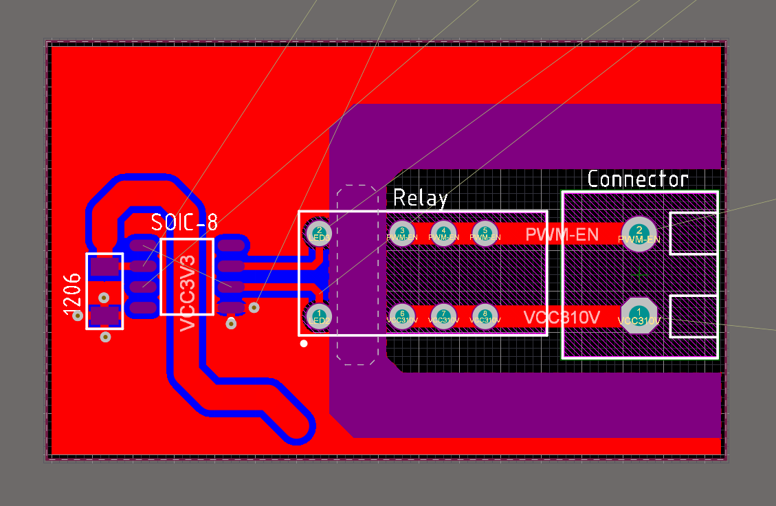
Rule number 6 - galvanic gap
Error - equating the dielectric gap to galvanic. In fact, they are very similar, but the requirements are stricter when it comes to galvanic isolation. A striking case is the decoupling of the control circuit and the power section using a relay or an optocoupler, when the gap between the decoupled sides is also chosen to be 0.8 or 1.5 mm.
Problem number 1 - insulation breakdown, failure of the control system and other expensive equipment.
Decision- increase the threshold electrical breakdown. Standard values are typically 1.5 kV, 2.5 kV and 4 kV. If your device works with mains voltage, but the person does not interact with it directly, then an isolation voltage of 1.5 kV will be sufficient. If a person is supposed to interact with the device, for example, through buttons and other controls, I recommend using insulation with a voltage of 2.5 kV or more.
Example:
1) Bad
What is wrong you ask, because there are gaps on the board, they can be made and 1.5 mm. The fact is that even if you make a gap of 2 mm, then this will not be enough to provide insulation. The “weakest” place should be the distance between the relay control terminals (1-2) and the power terminals (3-8). It is also necessary to take into account that the breakdown can be not only between conductors on the same layer, but also on different ones - through the board through fiberglass laminate.
2) Good What was done to improve the situation: a) There was a clear boundary between the low-voltage and high-voltage parts. Now the conductor + 3.3V does not pass in the high-voltage region + 310V, the GND test range does not go beyond the low-voltage part, respectively, and there will be no breakdown. Also, there should be nothing at all in the zone / boundary of the galvanic isolation.
b) The isolation zone is freed from the solder mask. The mask is also a weak point and, depending on the quality, will break through it before the glass fiber laminate. It is not necessary to do this in the general case, but if people interact with the device, I highly recommend it.
c) As I wrote above, the weak point is the distance between the control and power outputs of the relay. Everywhere I was able to make an insulating zone of 4 mm, and here only 2.5 mm. We cleared the mask, from the conductors, too, and the only thing that can breakdown on the board can happen is fiberglass laminate. Therefore, we remove it, I made a cutout under the 2.5 mm wide relay and removed the textolite between the leads. This operation is also not required, but it significantly increases the reliability and safety of your device.
Rule number 7 - Transition holes
Error - I often observe a picture when on a 2-layer printed circuit board in order to connect 2 pads, I use 3..4 ... or even 5 vias.
Problem number 1 - vias (via) becomes too much on the board and this limits the space for conductors, which leads to lengthening of the chains, and consequently to an increase in their resistance. Reduces the stability of circuits and interference signals.
Decision- use the minimum number of vias: if you need to connect 2 contacts on different layers, then do not use more than 1 vias. If 2 pins are on the same layer and you cannot connect them directly, then use a maximum of 2 vias. If you need more transitions to connect, then something you are doing wrong - train the logic and re-divide the section of the board that led to the problem.
Example:
1) Bad 2) Good The minimum number of vias (via) was used for the connection, which gives more space for other conductors and provides the minimum parasitic parameters of the conductor.
Some general tips
- Do not use autotrailers! In the "raw" not customized form, they give a terrible result, which even the brightest idea turns into a guano. In order for the autotracer to work well, it needs to prescribe certain rules that will tell him that the roads need not 0.15, but 1 mm, and so on. For an adequate result, even on simple boards you have to register a hundred, or even two, of these rules themselves. In Altium Designer, a whole section is allocated for them, for example. If you are an amateur and you are not up to the task of designing your own board for a laptop, then spread it out with your hands - it will be released faster and the quality will be at the height
- Do not be lazy to alter the fee. It often happens that you made a payment by 90%, but then everything became tight and you start breaking the “rules” and making guano. Roll back, sometimes you have to roll back to the very beginning, do the work efficiently and at the stage of debugging the device you will save a lot of time and nerves
- Before you start designing a board, look at several open source projects, for example, on habre or hackaday. The main thing is not to copy out other people's obvious mistakes.
- If you have any familiar electronics developers, let them be fans too - let them check. A fresh look at your project will avoid a lot of mistakes.
Conclusion
I hope this article will be useful for beginners electronics and save them at least from the most simple errors. I think quite a few people in these rules will see their shortcomings, but you should not blindly copy from this rule. Always think with your head and look for the best option, sometimes 4 vias for the 1st chain are acceptable, if it allows you to improve the final result.
Those who are not satisfied with this material - I propose to familiarize themselves with the IPC standards diagonally, it makes no sense to read much, as well as to read the initial course of “black magic” from Howard Jones. It also includes the physical design principles, as well as many recommendations on the design of standard circuits and interfaces. It used to be high-speed digital circuits that were something magical and sublime, but today even 2018 are in the courtyard of 2018 and even beginners are facing them, for example, when connecting sensors and memory via SPI or displays.