How processors are designed and manufactured: the future of computer architectures
- Transfer
Despite continuous improvements and gradual progress in each new generation, fundamental changes have not occurred in the processor industry for a long time. A huge step forward was the transition from vacuum to transistors, as well as the transition from individual components to integrated circuits. However, after them, serious paradigm shifts of the same magnitude did not occur.
Yes, transistors have become smaller, chips faster, and performance has increased hundreds of times, but we are starting to see stagnation ...
This is the fourth and final part of a series of articles on CPU development that talks about the design and manufacture of processors. Starting at a high level, we learned how computer code is compiled into assembly language, and then into binary instructions that the CPU interprets. We discussed how processor architecture is designed and they process instructions. Then we looked at the various structures that make up the processor.
A little deeper into this topic, we saw how these structures are created, and how billions of transistors work together inside the processor. We examined the process of physical manufacturing of processors from raw silicon. We learned about the properties of semiconductors and how the insides of a chip look like. If you missed any of the topics, here is a list of articles in the series:
Part 1: Fundamentals of computer architecture (instruction set architectures, caching, pipelines, hyperthreading)
Part 2: CPU design process (circuitry, transistors, logic elements, synchronization)
Part 3: Arrangement and physical production of the chip (VLSI and silicon fabrication)
Part 4 : Current trends and important future directions in computer architecture (sea of accelerators, three-dimensional integration, FPGA, Near Memory Computing)
Let's move on to the fourth part. The development companies do not share with the public their research or the details of modern technologies, so it is difficult for us to clearly imagine what exactly is inside the computer's CPU. However, we can take a look at modern research and find out in which direction the industry is moving.
One of the famous images of the processor industry is Moore's Law. It says that the number of transistors in a chip doubles every 18 months. For a long time, this rule of thumb was fair, but growth begins to slow. Transistors become so tiny that we begin to approach the limit of physically achievable sizes. Without a revolutionary new technology, we will have to explore other possibilities for productivity growth in the future.
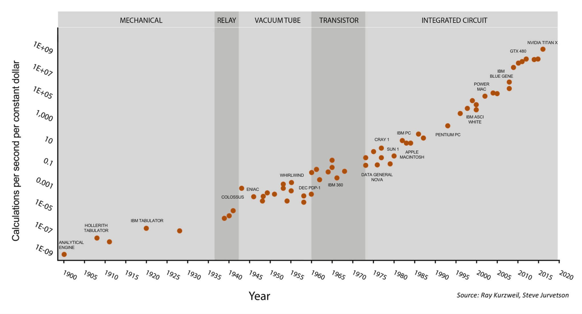
Moore's Law for 120 years. This graph becomes even more interesting if you find out that the last 7 points relate to the Nvidia GPU, and not to general-purpose processors. Illustration by Steve Jarvetson
One conclusion follows from this analysis: to increase productivity, companies began to increase the number of cores instead of frequency. For this reason, we are observing how eight-core processors are widely used, rather than dual-core processors with a frequency of 10 GHz. We just do not have much room left for growth, except the addition of new cores.
On the other hand, the field of quantum computing promises a huge space for future growth.. I am not a specialist, and since her technologies are still being developed, there are still few real "specialists" in this area. To dispel the myths, I will say that quantum computing will not be able to provide you 1000 frames per second in a realistic render, or something like that. So far, the main advantage of quantum computers is that they allow the use of more complex algorithms that were previously unattainable.
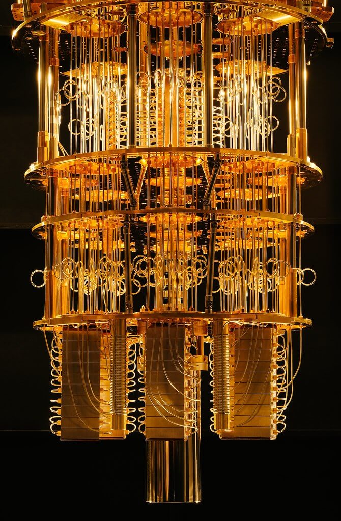
One of the prototypes of IBM quantum computers.
In traditional computers, the transistor is either on or off, which corresponds to 0 or 1. A superposition is possible in a quantum computer , that is, a bit can be simultaneously in states 0 and 1. Thanks to this new feature, scientists can to develop new calculation methods and they will have the opportunity to solve problems for which we still do not have enough computing power. The point is not so much that quantum computers are faster, but that they are a new computing model that will allow us to solve other types of problems.
There is still one or two decades left before the mass introduction of this technology, so what trends are we starting to see in real processors today? Dozens of active research is underway, but I will only touch on some areas that, in my opinion, will have the greatest impact.
The trend of the influence of heterogeneous computing is growing. This technique consists in incorporating many different computing elements into one system. Most of us take advantage of this approach as separate GPUs in computers. The central processor is very flexible and can with a decent speed perform a wide range of computing tasks. On the other hand, GPUs are designed specifically for graphical computing, such as matrix multiplication. They cope very well with this and are orders of magnitude faster than the CPU in such types of instructions. Transferring part of the graphic calculations from the CPU to the GPU, we can speed up the calculations. Any programmer can optimize the software by changing the algorithm, but optimizing the equipment is much more difficult.
But the GPU is not the only area in which accelerators are becoming more popular. Most smartphones have dozens of hardware accelerators designed to speed up very specific tasks. This style of computing is called the Sea of Accelerators , examples of which are cryptographic processors, image processors, machine learning accelerators, video encoders / decoders, biometric processors, and much more.
Loads are becoming more and more specialized, so designers are including more accelerators in their chips. Cloud service providers, such as AWS, have begun to provide developers with FPGA cards to accelerate their cloud computing. Unlike traditional computing elements like CPUs and GPUs, which have a fixed internal architecture, FPGAs are flexible. This is almost programmable equipment that can be customized to fit the needs of the company.
If someone needs image recognition, then he implements these algorithms in the hardware. If someone wants to simulate the work of a new hardware architecture, then before manufacturing it can be tested on FPGA. FPGA provides greater performance and energy efficiency than the GPU, but still less than the ASIC (application specific integrated circuit - a special purpose integrated circuit). Other companies, such as Google and Nvidia, are developing separate machine learning ASICs to speed image recognition and analysis.
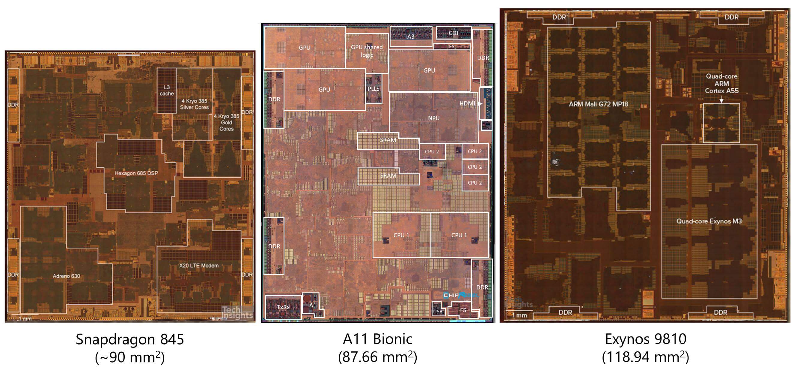
Crystal shots of popular mobile processors showing their structure.
Looking at the crystal images relative to modern processors, you can see that the core itself does not actually occupy the majority of the CPU area. Various accelerators take up a larger share. This made it possible to speed up very specialized calculations, as well as significantly reduce power consumption.
Previously, when it was necessary to add to the video processing system, developers had to install a new chip in it. However, it is very inefficient in terms of energy consumption. Each time a signal needs to exit a chip through a physical conductor to another chip, a huge amount of energy is required per bit. The tiny fraction of the joule itself does not seem to be a particularly big waste, but transferring data inside and not outside the chip can be 3-4 orders of magnitude more efficient. Thanks to the integration of such accelerators with the CPU, we have recently seen an increase in the number of chips with ultra-low power consumption.
However, accelerators are not ideal. The more we add them to the circuit, the less flexible the chip becomes and we begin to sacrifice overall performance in favor of the peak performance of specialized types of computing. At some point, the entire chip simply turns into a set of accelerators and ceases to be a useful CPU. The balance between specialized computing performance and overall performance is always very carefully tuned. This discrepancy between general purpose equipment and specialized loads is called the specialization gap .
Although some people think. Since we are at the peak of the GPU / Machine Learning bubble, we can most likely expect that more and more computing will be transferred to specialized accelerators. Cloud computing and AI continue to evolve, so GPUs look like the best solution to achieve the level of volumetric computing required.
Another area in which designers are looking for ways to increase productivity is memory. Traditionally, reading and writing values has always been one of the most serious bottlenecks in processors. Fast and large caches can help us, but reading from RAM or SSD can take tens of thousands of clock cycles. Therefore, engineers often see memory access as more expensive than the calculations themselves. If the processor wants to add two numbers, then it first needs to calculate the memory addresses by which the numbers are stored, find out at what level of the memory hierarchy there is this data, read the data into registers, perform calculations, calculate the receiver address and write the value to the right place. For simple instructions, which may take one to two cycles, this is extremely inefficient.
A new idea that is being actively explored is a technique called Near Memory Computing . Instead of retrieving small pieces of data from memory and computing them with a fast processor, the researchers turn the work upside down. They experiment with creating small processors directly in RAM or SSD memory controllers. Due to the fact that calculations are getting closer to memory, there is the potential for huge savings in energy and time, because data no longer needs to be transmitted so often. Computing modules have direct access to the data they need, because they are directly in memory. This idea is still in its infancy, but the results look promising.
One of the hurdles to overcome for near memory computing is the limitations of the manufacturing process. As stated in the third part , the silicon production process is very complex and involves dozens of stages. These processes are usually specialized for the manufacture of either fast logic elements or densely spaced storage elements. If you try to create a memory chip using a manufacturing process optimized for computing, you get a chip with an extremely low density of elements. If we try to create a processor using the drive manufacturing process, we get very low performance and large timings.

3D integration example showing vertical connections between transistor layers.
One potential solution to this problem is 3D integration . Traditional processors have one very wide layer of transistors, but this has its limitations. As the name implies, three-dimensional integration is the process of arranging several layers of transistors on top of each other to increase density and reduce delays. Vertical columns produced in different manufacturing processes can then be used for inter-layer joining. This idea was proposed a long time ago, but the industry has lost interest in it because of serious difficulties in its implementation. Recently, we are witnessing the emergence of 3D NAND storage technology and the revival of this area of research.
In addition to physical and architectural changes, another trend will strongly affect the entire semiconductor industry - a greater emphasis on security. Until recently, processor safety was thought almost at the last moment. This is similar to how the Internet, e-mail and many other systems that we actively use today were developed almost without regard to security. All existing protective measures were “screwed up” as incidents occurred, so that we feel safe. In the field of processors, such tactics have hurt companies, and especially Intel.
Bugs Specter and Meltdown are probably the most famous examples of how designers add features that significantly accelerate the processor, not fully aware of the security risks associated with this. In the development of modern processors, much more attention is paid to security as a key part of the architecture. When security is improved, performance often suffers, but given the damage that serious security bugs can cause, it can be safely said that it is better to focus on security to the same extent as on performance.
In the previous parts of the series, we touched on techniques such as high-level synthesis, which allows designers to first describe the structure in a high-level language, and then allow complex algorithms to determine the optimal hardware configuration for the function. With each generation, design cycles are becoming more expensive, so engineers are looking for ways to accelerate development. It should be expected that in the future this trend in hardware design with software will only intensify.
Of course, we are not able to predict the future, but the innovative ideas and areas of research considered by us in the article can serve as guidelines for expectations in the design of future processors. We can confidently say that we are nearing the end of the usual improvements to the manufacturing process. To continue to increase productivity in each generation, engineers will have to invent even more complex solutions.
We hope that our series of four articles has spurred your interest in studying the design, verification and production of processors. There is an infinite number of materials on this topic, and if we tried to reveal all of them, then each of the articles could grow into a whole university course. I hope you learned something new and now you better understand how sophisticated computers are at each level.