Review and refinement of devices from DreamSourseLab
I welcome everyone.
Following the traces of the previous articles on logical analyzers on Habré, I decided to finish my "fundamental" work.
I'll start a little from afar.
It all started in the early 10s, when I first found out about Saleae Logic (hereinafter referred to as Saleae, I mean an 8-channel analyzer without a slider) at some amateur radio forum.
Took note. But already at 13 in the process of implementing another project I came across the fact that I really needed a logic analyzer with a large buffer. The oscilloscope and hanteck la-5034 available at that time did not solve the problem.
The main feature of Saleae and its clones is the lack of a built-in buffer - the entire stream is immediately chased to the PC and saved there. Then it can be analyzed, decoded and exported. On the one hand, we are practically unlimited in depth of viewing (data can be stored for hours), on the other hand, the maximum sampling frequency is 24 MHz. In most cases, enough, however, due to the programmatic nature of sampling, the samples have a noticeable "jitter".
As a result, very quickly, in about a day, from Kharkov, from the 6-lab (now deceased), they sent me via clones their saleae clone with two eeproms already built in to switch the types of saleae and xbee (the hardware of these devices is the same only vid differs: pid which are flashed in eeprom).
Accordingly, you can use software from both manufacturers.
That's when I became interested in such a thing as СY7C68013A, well, or shorter than FX2 (although it is more correct than FX2LP).
This is an 8051-compatible microcontroller with a hardware USB2.0 port and honest 480Mb / s.
Features include: 16KB of RAM and the ability to download firmware both from a connected I2C EEPROM and via USB (there is no built-in flash there).
And this MK can pretend to be any device on the USB-bus (in the sense of responding to any VID: PID).
Some details from the datasheet on the loading procedure
Consider the case when an I2C EEPROM is connected to the MK.
In this case, the first 8 bytes are analyzed from it:
| EEPROM Address | Contents |
|---|---|
| 0 | 0xC0 |
| 1 | Vendor ID (VID) L |
| 2 | Vendor ID (VID) H |
| 3 | Product ID (PID) L |
| 4 | Product ID (PID) H |
| 5 | Device ID (DID) L |
| 6 | Device ID (DID) H |
| 7 | Configuration byte |
If the first byte is 0xC0 (as in the Saleae clone firmware), the MK configures the USB port with the VID: PID specified in 1-4 bytes and waits for the firmware to be downloaded via USB. Depending on the flashed VID: PID MK can "be" a different device, at least Saleae at least Xbee at least by someone. Very comfortably. You can solder the EEPROMs in a stack and select with a jumper.
But if the first byte is 0xC2, then starting with 9 bytes, the firmware for MK should be stored in EEPROM, which it will load into RAM and start executing.
The storage format is similar to Intel's HEX:
| 8 | Length h |
| 9 | Length l |
| 10 | Start Address H |
| eleven | Start Address L |
| - | Data block |
| - | Length h |
| - | Length l |
| - | Start Address H |
| - | Start Address L |
| - | Data block |
| - | 0x80 |
| - | 0x01 |
| - | 0XE6 |
| - | 0x00 |
| Last | 00000000 |
That is, the firmware is divided into blocks that are individually loaded into different sections of memory. And accordingly, it makes no sense to store empty areas.
And now we are smoothly approaching the main character of our article DreamSourseLab.
I won’t retell the whole story (I don’t really know it and do not see any deeper meaning). These are three engineers who, through crowdfunding, saw the project of the logical dream analyzer (almost).
What did they do.
They added to the FX2 a cheap plisina - Spartan 6 (maybe spied on Saleae).
And this is 16 channels at once, these are clear sampling points, this is the ability to pack individual bits (two lines can be sampled 4 times more often than 8, the main thing is to keep within the USB bandwidth). This is an opportunity to save to the buffer at a high frequency (400 MHz / 4 channels, 200 MHz / 8 channels, 100 MHz / 16 channels), and then slowly transfer it to a PC. And if you screw sigrok with its most powerful base of decoded protocols. In general, the project fired - everyone is happy. And taking into account the fact that the authors saved the stream mode (without saving to the internal buffer), we got a logical dream analyzer (well, almost because I immediately wanted 32 channels and FX3).
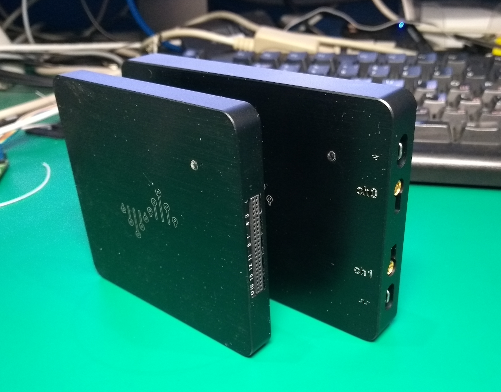
Thus appeared DSLogicPro. Strict black aluminum box with USB-C connector.
And then the engineers hit the business. And they released boxes with the name DSLogicBase and DSLogicPlus (as I understand it to conquer the world through Chinese sites), as well as DSCope (we hang a couple of 8-bit ADCs and now we have a two-channel oscilloscope).
Well, to keep this process under strict control, we changed the board layout a little. That is, the DSLogicPlus and DSLogicPro are electrically and functionally identical, but the SRAM hangs on the plug on the other pins (this is clearly seen in the picture of the tracks). I suspect that improvements have been made in other places.
By the way, a very valuable revision was made in terms of the cable for connecting the studied signals. If in Pro all 16 lines are connected at once with one wide connector, then in Plus, all cables were divided into groups of 4 channels that can be connected separately. Well, the cables themselves are short, coaxial and in the place of cutting (where the coaxial is divided into a separate signal and common wires) there is a small scarf with a filter.

And so, in the spring of 17, I ordered DSLogicBase in China (unfortunately, I didn’t know all that I wrote about then). They sent me everything, but looking forward to the 64 megasample buffer, I untwisted the board and saw an empty spot. Quickly raising the butchu returned 50% of the cost. And then he began to study the question of turning my Base into Plus. This is precisely the difference between Base and Plus - the presence of a separate buffer. Base uses memory built into the FPGA.
In the summer of 17, on the way to work and back for half an hour in the MCC train, I studied this issue. And pretty quickly it became clear that the differences were only in sealed SRAM and a pair of bytes of EEPROM firmware.
A little about what lies in the DSView / res directory
There we have a set of files with bin and fw extensions.
bin - these are firmware for plisina. They are loaded at the time of starting the program via fx2.
fw are binary firmware files for FX2.
If you compare all the fw files from it turns out that they all differ only in the PID byte at the address near the end.
That is, the differences between all devices are just this and the firmware of the plug (which, as I said, is loaded at the time of initialization).
Comparison of fw with what is written in the EEPROM (of course, I immediately dumped the dump from my analyzer) showed that the deployed firmware is here.
Если прошивку из EEPROM развернуть, то (насколько я помню) они совпадут (для версии ПО 0.96).
Таким образом, как уже писали на хабре, нужно всего лишь припаять память и в прошивке поменять 2 байта (в заголовке и потом далее в прошивке).
Аналогичным образом дорабатывается DSCope, допаиваем память и меняем PID в EEPROM.
Есть еще один нюанс.
По мере выпуска новых версий ПО (0.96-0.99) происходило добавление поддерживаемых моделей оборудования и изменение PID этих моделей.
Вот у меня получилась такая табличка:
| FW | Size buf | 0.96 | 0.97 | 0.98 | 0.99 | 0.98: 0x20 | 0.99: 0x20 |
|---|---|---|---|---|---|---|---|
| DSLogic | 256Mb | 01 | 01 | 01 | 01 | ||
| DSLogicPro | 256Mb | 1002 | 03 | 03 | 03 | 5 | 5 |
| DSMso | 05 | 05 | 05 | - | |||
| DSLogicBasic | 256Kb | 21 | 21 | 21 | 21 | 6 | 6 |
| DSLogicPlus | 256Mb | 20 | 20 | 20 | 20 | 6 | 6 |
| DSCope | 256Mb | 02 | 02 | 02 | 02 | ||
| DSCope20 | 256Mb | 04 | 04 | 04 | 04 | ||
| DSCope B20 | 256Mb | — | — | 22 | 22 | ||
| DSCope C20 | 256Mb | — | — | — | 23 | ||
| DSCope C20B | 256Mb | — | — | — | 24 | ||
| DSCope C20P | 256Kb | — | — | — | 25 |
In addition, some indication appeared in the firmware at address 0x20 for the Pro version there is 5, for Base and Plus there is 6. Most likely this is just the version of the printed circuit board.
By the way, there is another way to refine. No EEPROM reprogramming required. It is enough to solder SRAM, and then, when compiling libsigrok4DSL, make a correction to the file libsigrok4DSL / hardware / DSL / dsl.h:
In the structure describing the equipment static const struct DSL_profile supported_DSLogic [],
in the place where DSLogic PLus and Base are described, PID fields are interchanged so that the program thinks that it has Base PID 20 and Plus PID 21.
319     {0x2A0E, 0x0020, "DreamSourceLab", "DSLogic PLus", NULL,
320      "DSLogicPlus.fw",
321      "DSLogicPlus.bin",
322      "DSLogicPlus.bin",
323      {CAPS_MODE_LOGIC,
324       CAPS_FEATURE_VTH | CAPS_FEATURE_BUF,
325       (1 << DSL_STREAM20x16) | (1 << DSL_STREAM25x12) | (1 << DSL_STREAM50x6) | (1 << DSL_STREAM100x3) |
326       (1 << DSL_BUFFER100x16) | (1 << DSL_BUFFER200x8) | (1 << DSL_BUFFER400x4),
327       SR_MB(256),
328       0,
329       DSL_BUFFER100x16,
330       0,
331       0,
332       DSL_STREAM20x16,
333       SR_MHZ(1),
334       SR_Mn(1),
335       0,
336       0}
337     },
338
339     {0x2A0E, 0x0021, "DreamSourceLab", "DSLogic Basic", NULL,
340      "DSLogicBasic.fw",
341      "DSLogicBasic.bin",
342      "DSLogicBasic.bin",
343      {CAPS_MODE_LOGIC,
344       CAPS_FEATURE_VTH,
345       (1 << DSL_STREAM20x16) | (1 << DSL_STREAM25x12) | (1 << DSL_STREAM50x6) | (1 << DSL_STREAM100x3) |
346       (1 << DSL_BUFFER100x16) | (1 << DSL_BUFFER200x8) | (1 << DSL_BUFFER400x4),
347       SR_KB(256),
348       0,
349       DSL_STREAM20x16,
350       0,
351       0,
352       DSL_STREAM20x16,
353       SR_MHZ(1),
354       SR_Mn(1),
355       0,
356       0}
357     },
And your analyzer version with this version of DSView will work as if you had a real Plus.
In the meantime, I'll dream about a bunch of Spartan6 + FX3 + DSView.